I. INTRODUCTION
Organometal trihalide perovskite solar cells (PSCs) have attracted wide attention because such a solution process-based photovoltaic device has obtained comparable power conversion efficiencies (PCEs) (over 22%) with traditional commercial solar cells in a short time span of its development. 1–Reference Zhou and Zhu12 The special and advantageous optoelectronic properties of the hybrid materials (ABX3: A = CH3NH3, HC(NH2)2, Cs; B = Pb, Sn; X = Cl, Br, I) that account for the rapid growth in PCE, Reference Im, Jang, Pellet, Gratzel and Park7,Reference Sun, Salim, Mathews, Duchamp, Boothroyd, Xing, Sum and Lam13 include high mobility, Reference Ponseca, Savenije, Abdellah, Zheng, Yartsev, Pascher, Harlang, Chabera, Pullerits, Stepanov, Wolf and Sundstrom14–Reference Lim, Ahn, Kim, Qi and Lee17 long balanced carrier diffusion length, Reference Dong, Fang, Shao, Mulligan, Qiu, Cao and Huang15,Reference Shi, Adinolfi, Comin, Yuan, Alarousu, Buin, Chen, Hoogland, Rothenberger, Katsiev, Losovyj, Zhang, Dowben, Mohammed, Sargent and Bakr16,Reference Stranks, Eperon, Grancini, Menelaou, Alcocer, Leijtens, Herz, Petrozza and Snaith18,Reference Xing, Mathews, Sun, Lim, Lam, Gratzel, Mhaisalkar and Sum19 and low exciton binding energy. Reference D’Innocenzo, Grancini, Alcocer, Kandada, Stranks, Lee, Lanzani, Snaith and Petrozza20
Despite the high PCEs and the solution-based processes advantageous in commercializing PSCs, the poor device stability significantly hampered the application. The instability problem is caused not only by the perovskite itself but also by the conventional organic hole transport material (HTM), such as spiro-OMeTAD, PTAA, P3HT. Organic HTM layers are usually open and susceptible to migration of halide ions and metal ions (from the metal electrode), which inevitably result in device degradation. Reference Berhe, Su, Chen, Pan, Cheng, Chen, Tsai, Chen, Dubale and Hwang21–Reference Domanski, Correa-Baena, Mine, Nazeeruddin, Abate, Saliba, Tress, Hagfeldt and Grätzel27 Besides, most of these organic HTMs are expensive and operationally unstable (usually require inert atmosphere). Fortunately, researchers have proved that perovskites (e.g., CH3NH3PbI3) could serve as both a light harvester and a hole transporter, Reference Stranks, Eperon, Grancini, Menelaou, Alcocer, Leijtens, Herz, Petrozza and Snaith18,Reference Xing, Mathews, Sun, Lim, Lam, Gratzel, Mhaisalkar and Sum19,Reference Etgar, Gao, Xue, Peng, Chandiran, Liu, Nazeeruddin and Gratzel28,Reference Ku, Rong, Xu, Liu and Han29 thus facilitating HTM-free PSCs. Reference Ku, Rong, Xu, Liu and Han29–Reference Wei, Zheng, Chen, Long, Wang and Yang34
So far, several types of HTM-free PSCs have been developed with using Au, Reference Etgar, Gao, Xue, Peng, Chandiran, Liu, Nazeeruddin and Gratzel28,Reference Laban and Etgar35 Ni, Reference Ku, Xia, Shen, Tiep and Fan36 or carbon Reference Ku, Rong, Xu, Liu and Han29,Reference Wei, Yan, Chen, Yi, Zhang, Long, Li, Zhang, Wang and Yang37–Reference Chen and Yang39 as hole extraction electrodes. Due to the obvious advantageous properties of carbon electrodes, including low cost, high stability, inertia to ion migration, and high water resistance, carbon-based HTM-free PSCs (C-PSCs) have exhibited significantly higher stability than HTM-PSCs. Reference Wei, Zheng, Chen, Long, Wang and Yang34,Reference Zhou, Shi, Dong, Zhang, Xing, Wang, Du and Ma40 After the initial report in 2013, the PCE of C-PSCs has increased gradually from 6.64% to 15.9%, Reference Ku, Rong, Xu, Liu and Han29,Reference Mei, Li, Liu, Ku, Liu, Rong, Xu, Hu, Chen, Yang, Gratzel and Han30,Reference Chen and Yang41–Reference Chang, Li, Chen, Zhu, Liu, Geng, Xiang, Liu, Zheng, Yang and Yang47 which makes it among the most promising PSCs devices for commercialization. As a result, several research groups and companies have worked together to promote the commercialization of C-PSCs, and some scalable techniques have been exploited to fabricate large-scale devices.
Since great progresses have been achieved on the device stability and the scaling up of C-PSCs, herein, we aim to document these progresses to illustrate the promising prospect for their commercialization. Firstly, we will catalog and discuss the recent stability results of C-PSCs with an emphasis on a clear comparison with those of HTM-PSCs. Then, the research status on the large-scale C-PSCs will be appraised, including device structures and scalable techniques. Finally, main issues and future research directions will be addressed.
II. DEVICE STRUCTURES AND WORKING PRINCIPLES OF C-PSCS
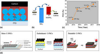
As illustrated in Fig. 1(a), C-PSCs usually consist of FTO/TiO2 dense layer/TiO2 mesoporous layer/perovskite/carbon. The general working principles of C-PSCs are illustrated in Fig. 1(b). After light illumination, electrons and holes are produced in the conduction band (CB) and valence band (VB) of the perovskite, respectively. The photogenerated electrons produced in the CB of the perovskite are subsequently injected into the CB of TiO2 and transported to the FTO substrate, while the photogenerated holes in the VB of the perovskite are extracted by carbon electrodes. The initial work was reported by Ku et al. in 2013, which achieved a PCE of about 6.6% [Fig. 1(c)]. Reference Ku, Rong, Xu, Liu and Han29 After one year, they further push the PCE to 12.8%. Reference Mei, Li, Liu, Ku, Liu, Rong, Xu, Hu, Chen, Yang, Gratzel and Han30 In 2016, Chen et al. boosted the PCE to 14.38%. Reference Sheng, Hu, Mei, Jiang, Hou, Duan, Hong, Guan, Rong, Xiong and Han48 Very recently, Zhang et al. have promoted the PCE to 15.9%. Reference Zhang, Wang, Williams, Xiong, Zhang, Chueh, Chen and Jen43
Device structure, working principle and efficiency evolution of C-PSCs. (a) Structure of C-PSCs, (b) schematic energy level diagram and charge transfer behavior in C-PSCs, (c) reported efficiency evolution of C-PSCs, and (d) structure and fabrication processes of three types of C-PSCs. Reprinted with permission from Refs. Reference Ku, Rong, Xu, Liu and Han29, Reference Chen and Yang41, and Reference Chen, Wei, He, Zheng, Wong and Yang46. Copyright 2013, Nature Publishing Group. Copyright 2017, Wiley. Copyright 2016, Wiley.

According to the device structure and fabrication procedure, C-PSCs could be divided into three types: meso C-PSCs, embedment C-PSCs, and paintable C-PSCs (Fig. 1). Reference Chen and Yang41 Meso PSCs, developed by Ku et al [Fig. 1(d)], Reference Ku, Rong, Xu, Liu and Han29 comprise of a multi-layer mesoporous structure, followed by the infiltration of a perovskite solution. Reference Ku, Rong, Xu, Liu and Han29,Reference Chan, Wang, Wu and Diau49 Embedment C-PSCs were explored by Wei et al., Reference Wei, Yan, Chen, Yi, Zhang, Long, Li, Zhang, Wang and Yang37 in which the carbon electrode was deposited onto a predeposited PbI2 layer, followed by postconverting PbI2 to MAPbI3. Paintable C-PSCs were originated from the clamping concept reported in the initial paper on embedment C-PSCs, Reference Zhang, Yang, Wang, Cheng, Zhao and Sun32,Reference Wei, Yan, Chen, Yi, Zhang, Long, Li, Zhang, Wang and Yang37,Reference Zhou, Shi, Dong, Zhang, Xing, Wang, Du and Ma40 in which the carbon electrode in paste or paint form is deposited on a perovskite layer using either a painting process or a doctor blade technique, at low temperature. Though all these C-PSCs operate via similar charge transport principles, their different device structures and fabrication processes have led to significantly different photovoltaic performance.
III. THE HIGH STABILITY OF C-PSCS
The first reported C-PSCs are the well-known meso C-PSCs developed by Ku et al., Reference Ku, Rong, Xu, Liu and Han29 which have a typical multi-layer mesoporous structure, including TiO2, ZrO2, and porous carbon layers, serving as the electron transporting layer, insulating layer, and hole extraction layer, respectively. The TiO2 and ZrO2 mesoporous layers in these meso C-PSCs were fabricated from nanoparticles, while the carbon mesoporous layer (at least several micrometers thick) was carbon black and layered graphite. Finally, a perovskite precursor solution was infiltrated into the multi-layer mesoporous structure by applying the precursor solution dropwise to the surface to obtain the meso C-PSCs.
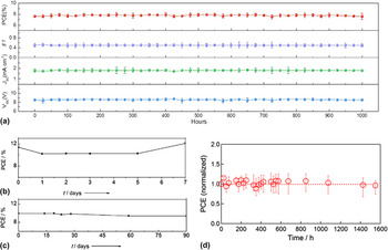
The ultra-high stability is the obvious advantage of meso C-PSCs. The initial meso C-PSCs fabricated from the MAPbI3 perovskite solution containing PbI2 and MAI exhibited almost no performance decay after storage in dark (dry air and room temperature) for 840 h. Reference Ku, Rong, Xu, Liu and Han29 by introducing HOOC(CH2)4NH3I (5-AVAI) into the precursor solution to partially replace MAI, the obtained mixed perovskite of (5-AVA) x (MA)1−x PbI3 not only significantly improved pore filling capacity to promote the PCE to 12.8% but also greatly improved the device stability. Reference Ku, Rong, Xu, Liu and Han29,Reference Chen, Wu, Yue, Liu, Zhang, Yang, Chen, Bi, Ashraful, Gratzel and Han50 Both the large and small nonencapsulated devices retained their initial photovoltaic performance after light soaking in an air atmosphere for over 1000 h [Fig. 2(a)].
Stability testing results of C-PSCs. (a) Photovoltaic change with time under light soaking (AM 1.5, 100 mW/cm2) in ambient air. Reprinted with permission from Ref. Reference Hu, Si, Mei, Rong, Liu, Li and Han53. Copyright 2017, Wiley. (b) PCE variation of encapsulated meso C-PSCs during outdoor aging in Jeddah, Saudi Arabia and (c) PCE variation of encapsulated meso C-PSCs in ambient air at 80–85 °C. Reprinted with permission from Ref. Reference Li, Tschumi, Han, Babkair, Alzubaydi, Ansari, Habib, Nazeeruddin, Zakeeruddin and Gratzel51. Copyright 2015, Wiley. (d) Normalized PCE variation of encapsulated meso C-PSCs in ambient air at 100 °C. Reprinted with permission from Ref. Reference Baranwal, Kanaya, Peiris, Mizuta, Nishina, Kanda, Miyasaka, Segawa and Ito52. Copyright 2016, Wiley.

Such a high stability of the C-PSCs foreshadows the opportunity for their commercialization. To verify the commercializing feasibility and potential, Li et al. have comprehensively investigated the stability of such devices by means of both practical and accelerated tests. Reference Li, Tschumi, Han, Babkair, Alzubaydi, Ansari, Habib, Nazeeruddin, Zakeeruddin and Gratzel51 During outdoor aging in Jeddah, Saudi Arabia, the device performed adequately after 7 days [Fig. 2(b)]. Following storage in a dark, normal oven under ambient air at 80–85 °C for 90 days, no obvious PCE decay was observed [Fig. 2(c)]. More promisingly, a systematic stability evaluation conducted by Baranwal et al. showed that almost no PCE degradation was observed for encapsulated meso C-PSCs in ambient air at 100 C [Fig. 2(d)]. Reference Baranwal, Kanaya, Peiris, Mizuta, Nishina, Kanda, Miyasaka, Segawa and Ito52 These promising results on stability confirmed that meso C-PSCs could provide a promising path toward realizing efficient and stable PSCs.
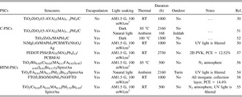
The above-mentioned device stability is considerably higher than those of HTM-PSCs, which is the most advantageous feature of C-PSCs. To highlight this advantage, we have collected some representative stability testing results on HTM-PSCs and C-PSCs for a clear comparison (Table I). Obviously, higher photo stability and thermal stability were demonstrated of C-PSCs, especially under harsh testing conditions (AM1.5 G, 100 mW/cm2, and 85–100 °C). Reference Mei, Li, Liu, Ku, Liu, Rong, Xu, Hu, Chen, Yang, Gratzel and Han30,Reference Li, Tschumi, Han, Babkair, Alzubaydi, Ansari, Habib, Nazeeruddin, Zakeeruddin and Gratzel51–Reference Hu, Si, Mei, Rong, Liu, Li and Han53 Moreover, promising outdoor stability results have also been achieved (under hot and high humid climate at Jeddah, Saudi Arabia). Reference Li, Tschumi, Han, Babkair, Alzubaydi, Ansari, Habib, Nazeeruddin, Zakeeruddin and Gratzel51 However, for HTM-PSCs, most of the stability testing conditions were modified, and promising thermal stability has been rarely reported. For example, several researches have used a filter to remove the UV light from the incident illumination by using a glass filter or polymer coating. Reference Chen, Wu, Yue, Liu, Zhang, Yang, Chen, Bi, Ashraful, Gratzel and Han50,Reference Bella, Griffini, Correa-Baena, Saracco, Grätzel, Hagfeldt, Turri and Gerbaldi54,Reference Tan, Jain, Voznyy, Lan, Garcia de Arquer, Fan, Quintero-Bermudez, Yuan, Zhang, Zhao, Fan, Li, Quan, Zhao, Lu, Yang, Hoogland and Sargent55 Some other researches have conducted the stability measurement in N2 atmosphere, which is far from ambient atmosphere. Reference Tan, Jain, Voznyy, Lan, Garcia de Arquer, Fan, Quintero-Bermudez, Yuan, Zhang, Zhao, Fan, Li, Quan, Zhao, Lu, Yang, Hoogland and Sargent55,Reference Saliba, Matsui, Domanski, Seo, Ummadisingu, Zakeeruddin, Correa-Baena, Tress, Abate, Hagfeldt and Gratzel56 The exploitation of two dimensional (2D) perovskite and all inorganic collection layers seem to have improved the device stability of HTM-PSCs, but the PCE was well suppressed. Reference Tsai, Nie, Blancon, Stoumpos, Asadpour, Harutyunyan, Neukirch, Verduzco, Crochet, Tretiak, Pedesseau, Even, Alam, Gupta, Lou, Ajayan, Bedzyk, Kanatzidis and Mohite57 Moreover, thermal stability in ambient atmosphere has not been reported yet, indicating that the road to commercializing HTM-PSCs is far from that of C-PSCs.
Representative stability testing data reported of C-PSCs and HTM-PSCs.

In parallel, embedment C-PSCs and paintable C-PSCs have also demonstrated considerably high stability. The embedment C-PSCs were mainly prepared and investigated by Yang’s group, Reference Wei, Chen, Yan and Yang31,Reference Wei, Yan, Chen, Yi, Zhang, Long, Li, Zhang, Wang and Yang37,Reference Chen, Wei, Yan, Yi, Wang and Yang38,Reference Zheng, Chen, Li, Yang, Wei, Bai, Qiu, Zhou, Wong and Yang44,Reference Wei, Chen, Yan, Zheng and Yang59 which indicated that these devices could retain its performance after storage in dark conditions for tens of days. Very recently, results on the embedment C-PSCs based on B-doped multi wall carbon nanotubes indicated that these devices not only could get a high PCE of 15.23% but also exhibited a considerably high stability, which could retain their performance at room temperature in air for 80 days and at 80 °C for 14 days. Reference Zheng, Chen, Li, Yang, Wei, Bai, Qiu, Zhou, Wong and Yang44
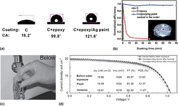
Since the carbon electrode in paintable C-PSCs is composed of carbon materials and polymer additives, the wettability of the carbon electrode is reduced [Fig. 3(a)], which could smoothen the serious attack from surrounding water molecules. Therefore, the paintable C-PSCs usually exhibited a high stability in ambient conditions or even under water. Reference Zhang, Yang, Wang, Cheng, Zhao and Sun32,Reference Wei, Zheng, Chen, Long, Wang and Yang34,Reference Zhou, Shi, Dong, Zhang, Xing, Wang, Du and Ma40 For example, a custom carbon paint developed by Zhou et al. resulted in a no PCE decay of a nonencapsulated device after 2446 h. Reference Zhou, Shi, Dong, Zhang, Xing, Wang, Du and Ma40 Besides, Wei et al. demonstrated that the carbon electrodes with epoxy well improved the performance stability under water immersion, and after further forming a hydrophobic Ag coating from Ag paint, the performance could retain most of the initial PCE for over 1 h. Reference Wei, Zheng, Chen, Long, Wang and Yang34 Furthermore, Yu et al. demonstrated that about 98 and 92% of the initial PCE of their devices were retained after exposing the paintable C-PSCs to water flushing [Figs. 3(c) and 3(d)], respectively. Reference Yu, Chen, Liu, Wang, Bu, Cheng, Bai, Yan and Zhao60 Though many reported paintable C-PSCs have shown excellent stability, stability testing under more practical conditions, such as light soaking conditions, high temperature (e.g., 80 °C), etc., is still lacking.
Stability of C-PSCs under water. (a) Contact angle photographs of three electrodes: pure carbon, carbon/epoxy, and carbon/epoxy/Ag paint and (b) Normalized efficiency as a function of soaking time in water (measured by recording J–V curves of the PSCs immersed in water). Reprinted with permission from Ref. Reference Wei, Zheng, Chen, Long, Wang and Yang34. Copyright 2015, Royal Chemical Society. The inset shows the measurement setup. (c) Photograph of the as-prepared PSCs placed under running water, and (d) J–V curves of the as-prepared C-PSCs before and after water exposure. Reprinted with permission from Ref. Reference Yu, Chen, Liu, Wang, Bu, Cheng, Bai, Yan and Zhao60. Copyright 2016, Wiley.

IV. SCALING UP OF C-PSCS
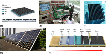
Since C-PSCs have demonstrated considerably high stability together with decent PCEs, some groups and companies are considering scaling up the device production. However, conventional spin coating technique was only suitable for small-area devices, which could not be simply scaled up. The special architecture and fabrication process of meso C-PSCs facilitates the use of scalable screen-printing technique for automated production. The most recent demonstrated meso C-PSCs were illustrated in Fig. 4(a), in which batch processing on rigid glass substrates was realized by screen-printing techniques [shown in Fig. 4(b)]. Reference Hu, Si, Mei, Rong, Liu, Li and Han53,Reference Priyadarshi, Haur, Murray, Fu, Kulkarni, Xing, Sum, Mathews and Mhaisalkar61 The final solar cell module was exhibited in Fig. 4(c), which has achieved a PCE over 10% for large active areas of 70 and 49 cm2 (Table II). Reference Hu, Si, Mei, Rong, Liu, Li and Han53,Reference Priyadarshi, Haur, Murray, Fu, Kulkarni, Xing, Sum, Mathews and Mhaisalkar61 Hu et al. have made a more forward step to enlarge the module area to 7 m2, which could be directly used to power a panel. Reference Hu, Si, Mei, Rong, Liu, Li and Han53 All these achievements have implied the nearest term for PSCs commercialization. For practical application, auto production line needs to be developed for enabling continuous and controllable fabrication process of the module. The proposed production line has also been given by Hu et al. in Fig. 4(d). Reference Hu, Si, Mei, Rong, Liu, Li and Han53 As indicated, the conduction glasses were first etched by laser, followed by the sequential deposition of compact TiO2, mesoporous TiO2, mesoporous ZrO2, and mesoporous carbon layers by screen printing. Finally, perovskite solution could be deposited by screen printing, doctor blade, or inkjet printing technique.
Fabrication of large-scale meso C-PSCs. (a) Structure scheme of solar module. Reprinted with permission from Ref. Reference Hu, Si, Mei, Rong, Liu, Li and Han53. Copyright 2017, Wiley. (b) Photograph of semi-automatic screen printer and (c) meso C-PSCs module prepared by screen printer. Reprinted with permission from Ref. Reference Priyadarshi, Haur, Murray, Fu, Kulkarni, Xing, Sum, Mathews and Mhaisalkar61. Copyright 2016, Royal Chemical Society. (d) Solar panel of meso C-PSCs, and (e) schematic illustration of the proposed production line of meso C-PSCs. Reprinted with permission from Ref. Reference Hu, Si, Mei, Rong, Liu, Li and Han53. Copyright 2017, Wiley.

Reported data for large-scale C-PSCs.

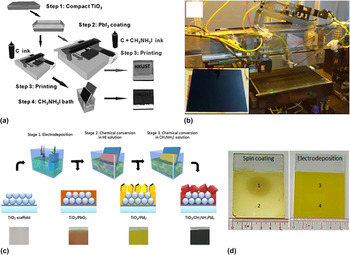
Several other techniques have also been exploited for large-scale fabrication of C-PSCs. For the large-scale deposition of carbon electrodes, Wei et al. have exploited inkjet printing techniques to deposit carbon electrodes in embedment C-PSCs. Reference Wei, Chen, Yan and Yang31 Two strategies have been designed to realize the idea. The first one is that carbon could be directly deposited on the PbI2 layer, followed by postconversion to perovskite. The other one is ingenious, in which carbon/MAI ink was developed. During inkjet printing, carbon electrodes and chemical conversions happened simultaneously, which obviated the predeposition process of carbon electrodes. Reference Wei, Chen, Yan and Yang31 The application of inkjet printing makes the deposition of carbon electrodes scalable and controllable. Besides, this strategy resulted in an interpenetrating interface between MAPbI3 and carbon electrodes for deducing charge recombination and increasing PCE. As reported afterward, perovskite layer could also be deposited by inkjet printing, Reference Li, Jiang, Su, Cui, Huang, Zhang, Zhou, Yang and Song62 which further made the inkjet printing technique more promising for scaling up the C-PSCs.
For the production of C-PSCs or PSCs, the processes developed for OPVs could also be adaptable. As a compatible technique with a roll-to-roll, slot-die coating technology, that is, a noncontact large-area fabrication technique has achieved success in large-scale OPVs fabrication. As a result, slot-die coating technology has been also exploited to deposit perovskite layer in PSCs. Reference Hwang, Jung, Heo, Scholes, Watkins, Subbiah, Jones, Kim and Vak63 Recently, Weihua-Solar Company used a slot-die coating technology to produce large-scale perovskite layers for paintable C-PSCs (ZnO/MAPbI3/C) panels as shown in Fig. 5(b), which could be easily scaled up (such as 45 × 65 cm). Reference Zhou and Zhu12 The 25 cm2 modules achieved a promising PCE of 10.6% with a negligible degradation after 140 days of outdoor testing. Reference Longhua, Lusheng, Jifeng, Bin, Lili and Bin64
Some reported scaling-up techniques for the fabrication of C-PSCs. (a) Inkjet printing. Reprinted with permission from Ref. Reference Wei, Chen, Yan and Yang31. Copyright 2014, Wiley. (b) Slot-die coating technology. Reprinted with permission from Ref. Reference Zhou and Zhu12. Copyright 2016, American Chemical Society. (c) Electrodeposition, and (d) photographs of the large-scale PbI2 precursors prepared by spin coating and electrodeposition. Reprinted with permission from Ref. Reference Chen, Wei, Zheng and Yang33. Copyright 2015, Elsevier.

Besides, Chen et al. have developed a mature electrodeposition strategy to deposit the PbI2 precursor on TiO2 scaffold, Reference Chen, Wei, Zheng and Yang33 as shown in Fig. 5(c). Firstly, electrodeposition technique was applied to deposit PbO2. Then, PbO2 was converted to PbI2 by the immersion in HI ethanol solution. Finally, PbI2 was converted to dark brown colored MAPbI3 in MAI solution. This whole low-temperature electrodeposition procedure was obviously scalable in substrate size, as shown in Fig. 5(d). In addition, this technique was flexible for a variety of disparate substrate shapes and forms and was roll-to-roll compatible. In combination with the painting process for carbon electrode deposition, the paintable C-PSCs could be easily scaled up. The large-scale paintable C-PSCs (4 cm2) fabricated by these electrodepositions and painting techniques achieved a promising PCE of 4.47% (Table II).
V. PENDING ISSUES AND FUTURE RESEARCH DIRECTIONS
In spite of the obviously higher stability of C-PSCs than HTM-PSCs, the stability of C-PSCs is still significantly lower than that of silicon and thin film solar cells, which calls for more efforts to further improve the stability before their commercialization. So far, more works on C-PSCs are based on MAPbI3 perovskites, whose stability is not high. To further improve the stability of C-PSCs, new and more stable mixed perovskites should be exploited, such as FA0.81MA0.15PbI2.55Br0.45, Reference Li, Bi, Yi, Decoppet, Luo, Zakeeruddin, Hagfeldt and Gratzel2 Cs0.05FA0.81MA0.14PbI2.55Br0.45, Reference Bella, Griffini, Correa-Baena, Saracco, Grätzel, Hagfeldt, Turri and Gerbaldi54 Rb0.05(Cs0.05(MA0.17FA0.83)0.95)0.95(I0.83Br0.17)3, Reference Saliba, Matsui, Domanski, Seo, Ummadisingu, Zakeeruddin, Correa-Baena, Tress, Abate, Hagfeldt and Gratzel56 and so on. Since ultraviolet (UV) light would induce severe degradation of perovskites, the application of UV light filter coating may be a promising approach. For example, by coating a luminescent photopolymer layer on the front side of an FTO glass, UV light was absorbed to re-emit in the visible range to both increase photocurrent and avoid UV-induced degradation. Reference Bella, Griffini, Correa-Baena, Saracco, Grätzel, Hagfeldt, Turri and Gerbaldi54 Besides, to increase the humidity resistance of C-PSCs, the modification of the carbon electrode with superhydrophobic molecules could be another choice to enhance the device stability.
Though some scaling-up techniques have been developed to prepare a large-area perovskite layer for C-PSCs, the challenge remains to be able to consistently form a uniform, high-purity perovskite layer at large scale due to the difficulty in controlling crystallization behavior, which still significantly limits the PCE of C-PSCs modules. Therefore, the future development and optimization of large-scale deposition technologies is needed to accelerate the commercialization of C-PSCs. In fact, some successful researches on post treatment seem to have spotted a light on solving this issue. Typically, MA gas treatment on the predeposited MAPbI3 layer has been proved to considerably improve the film morphology and crystal quality, Reference Zhou, Wang, Zhou, Pang, Wang, Xu, Liu, Padture and Cui65 which is attributed to the formation of high-liquidity MAPbI3·xMA intermediate phase for inducing a reconstruction to get a smooth and uniform film. Reference Zhou, Wang, Zhou, Pang, Wang, Xu, Liu, Padture and Cui65,Reference Pang, Zhou, Wang, Yang, Krause, Zhou, Zhu, Padture and Cui66 Besides, NH3, Reference Zhao and Zhu67 DMF, Reference Xiao, Dong, Bi, Shao, Yuan and Huang68 and DMSO, Reference Wu, Chen, Yue, Liu, Bi, Yang, Islam and Han69 gas treatment has also shown a positive effect on improving the morphology and crystal quality of the perovskite layer, which may be exploited to increase the quality of the large-scale perovskite layer. In addition, the series resistance of the FTO glass and carbon electrode should be reduced to improve the FF and PCE of large-area C-PSCs.
VI. CONCLUSIONS
We have summarized the recent progresses on the device stability and the scaling up of C-PSCs. The different types of C-PSCs, including meso C-PSCs, embedment C-PSCs, and paintable C-PSCs have exhibited significantly high stability, which is still being improved steadily. In addition, due to the high water resistance property of the carbon electrode, some C-PSCs could even work well under water immersion or water flushing. Since the mesoporous layers in meso PSCs could be deposited by scalable screen-printing techniques, the large-scale meso C-PSCs with high performance have been well fabricated and reported. In addition to screen printing, other promising scalable techniques, including inkjet printing, slot-die coating, and electrodeposition have also been exploited for the large-scale fabrication of C-PSCs. Though great progresses have been achieved, some issues on device stability and scaling-up production still need to be addressed to further promote the commercialization of C-PSCs.
ACKNOWLEDGMENTS
This work is financially supported by the Young Talent of “Zhuoyue” Program of Beihang University, the National Natural Science Foundation of China (Nos. 51371020 and 21603010), the HK-RGC General Research Funds (GRF Nos. 16312216 and 16300915), and the HK Innovation and Technology Fund (ITS/219/16).