Introduction
Composite and single-phase multiferroic materials, such as Ni1−xZnxFe2O4/lead zirconate titanate multilayers and single-phase BiFeO3,Reference Srinivasan1 have been a major research focus of late due to their versatile functionalities for a wide range of applications that take advantage of its strong magnetoelectric (ME) coupling.Reference Eerenstein, Mathur and Scott2–Reference Ma, Hu, Li and Nan8 Multiferroic materials are defined as having two or more of the ferroic properties such as ferroelectricity, ferromagnetism, and ferroelasticity, where “single-phase” indicates that a single material has two or more of the ferroic properties. Currently, multiferroic composites lead the field due to their ME coupling coefficients being several orders of magnitude higher than those of single-phase multiferroics. The strong ME coupling effect in multiferroic materials has demonstrated good energy conversion between electric and magnetic fields, allowing for practical multiferroic devices such as sensors and tunable radio-frequency (RF)/microwave devices.
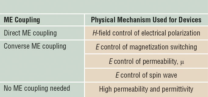
Multiferroic devices can be categorized based on the control mechanism, as shown in Table I. There are two types of ME coupling effects used for practical devices—direct and converse ME coupling. Direct ME coupling (magnetic field control of electrical polarization) has been used in magnetometers and energy harvesters.Reference Dong, Li and Viehland9,Reference Dong, Zhai, Li, Viehland and Priya10 Converse ME coupling (with electric-field control of magnetization switching can be used in spintronics, ME random access memory, and other applications.Reference Liu, Li, Obi, Lou, Rand and Sun11–Reference Nan, Zhou, Lou, Liu, Yang, Gao, Rand and Sun13 Converse ME coupling (with electric-field control of magnetic permeability and spin waves has been used in voltage tunable inductors, tunable bandpass filters, and tunable phase shifters. Multiferroic materials with high permeability and high permittivity provide great opportunities for compact RF/microwave devices such as miniature antennas. Finally, a combination of direct and converse ME coupling is required to realize ME antennas used for both receiving and transmitting. In this article, integrated magnetic tunable inductors, tunable RF bandpass filters with nanoelectromechanical systems (NEMS) ME resonators, RF NEMS direct current (DC) magnetic field ME sensors, and novel NEMS ME antennas will be presented.
Classification of magnetoelectric coupling.

Note: ME, magnetoelectric; H, magnetic; E, electric.
Voltage tunable RF/microwave integrated ME inductors
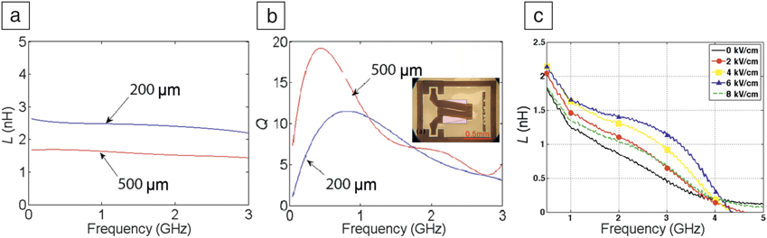
As one of the three fundamental components for electronic circuits, inductors have been used extensively in a variety of RF applications. However, it has been challenging to achieve enhanced inductance and quality factor (Q = ω × maximum energy stored/power loss, ω is the angular frequency) at RFs, particularly for GHz frequencies. Gao demonstrated high-Q integrated magnetic inductors based on a solenoid structure with multilayer FeGaB/Al2O3 films.Reference Gao, Zardareh, Yang, Nan, Zhou, Onabajo, Liu, Aronow, Mahalingam, Howe, Brown and Sun14 The high-quality factor was obtained because of the demonstrated eddy-current loss reduction, lower out-of-plane anisotropy, and higher permeability in comparison with a single FeGaB layer of the same thickness. The inductors exhibit significantly enhanced and flat inductance, as well as a high-quality factor at 0.5–2.5 GHz, showing great potential for RF integrated circuit (RFIC) applications. Figure 1a–b shows the frequency dependence of the inductance and quality factor, respectively, for two different lengths of magnetic film (200 and 500 μm).Reference Gao, Zardareh, Yang, Nan, Zhou, Onabajo, Liu, Aronow, Mahalingam, Howe, Brown and Sun14 Nearly constant inductance across 0.1 to 3 GHz with a high-quality factor of 19 at 0.5 GHz are presented, where the Q is normally around 10 at this frequency range for integrated RF inductors. The lower resistance loss and higher quality factor are due to the increased coil winding width needed for the increased magnetic core length. Because the number of turns to cover the core and the gap between two neighboring coils remain constant, a longer core length necessitates a wider coil, and with the wider coil, the current can pass more easily, thus lowering the resistance.
Comparison between different lengths of the FeGaB/Al2O3 film (200 μm and 500 μm): (a) Inductance, L, and (b) quality factor, Q. The inset shows the optical image of the inductor. (c) By applying various electric fields to the Pb(Mg1/3Nb2/3)O3–PbTiO3 slab, high tunability of inductance, which reaches up to 150% in approximately 2–3.5 GHz, can be achieved.Reference Gao, Zardareh, Yang, Nan, Zhou, Onabajo, Liu, Aronow, Mahalingam, Howe, Brown and Sun14

In order to directly transfer the strain to the inductor and enhance the performance, deep reactive-ion etching was applied to remove the Si substrate on the back side, and the inductors were bonded with ethyl cyanoacrylate glue to one piezoelectric single crystal of the Pb(Mg1/3Nb2/3)O3–PbTiO3 (PMN-PT) slab poled along its thickness direction (thickness of ∼0.5 mm).Reference Gao, Zare, Onabajo, Li, Zhou, Nan, Yang, Liu, Mahalingam, Howe, Jones and Sun15 Due to the strain-mediated magnetoelectric coupling, large inductance tunability (up to 150%) from 2 GHz to 3.5 GHz was achieved in the inductors with an applied E-field ranging from 0 to 8 kV/cm across the thickness direction of the PMN-PT slab, as shown in Figure 1c. The ME inductor showed good high-frequency performance with a wide operation frequency range, in which the inductance is more than 2 nH and the peak quality factor is close to 20. This shows great promise for voltage tunable inductance in RFIC.
Dual magnetic- and electric-field tunable nanoelectromechanical systems ME bandpass filters
RF bandpass filters based on thin-film bulk acoustic resonators (FBARs) show a high-quality factor, compact size, low loss, preferable temperature stability, and processing compatible with the complementary metal oxide semiconductor (CMOS) integrated circuit, which are widely used in smartphones and e-readers. However, these FBAR-based bandpass filters have a fixed frequency of operation, which lead to bulky and expensive electronics for reconfigurable communication systems. Here, high-quality factor miniaturized RF bandpass filters (device or circuit that allows signals between two specific frequencies to pass, but discriminates against signals at other frequencies) with dual electric (E-) and magnetic (H-)field tunability based on ME nanoelectromechanical systems (NEMS) coupled FBARs using a five-mask microfabrication process were fabricated.Reference Lin, Nan, Qian, Gao, Hui, Wang, Guo, Belkessam, Shi, Rinaldi and Sun16 Due to the strong ME effect between the piezomagnetic multilayer FeGaB/Al2O3 films and piezoelectric AlN thin film, the acoustic wave could be strongly coupled with the electromagnetic wave. The resonance of coupled resonators, which are excited in the fundamental, longitudinal mode, and the transmission from port one to port two along the in-plane direction, are due to the contour mode, or in-plane mode, which is mainly determined by the width of the resonator.
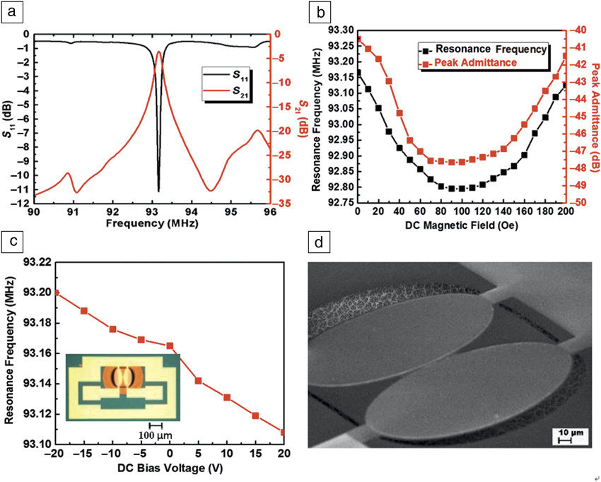
An 11.15 dB return loss, the loss of power in the returned/reflected signal, and 3.57 dB insertion loss, the loss of signal power resulting from the insertion, with a high-quality factor of 252 can be achieved at 93.165 MHz at zero-bias field, as shown in Figure 2a.Reference Lin, Nan, Qian, Gao, Hui, Wang, Guo, Belkessam, Shi, Rinaldi and Sun16 The bandpass filters have a sensitive dependence on the magnetic field with ∼0.5% magnetic field tunability (∼50 kHz/10 Oe) of the operation frequency as seen in Figure 2b. The delta-E effect, which is a change in the Young’s modulus causing a change in frequency, is determined by the total anisotropy that includes the shape anisotropy and the induced anisotropy. This reached a maximum under ∼95 Oe applied magnetic field. Figure 2c shows a voltage tunability of 2.3 kHz/1 V. The shift in the frequency due to ME coupling is relatively small compared with the delta-E effect, since the magnetostriction coefficient of FeGaB, 70 ppm, is much smaller than the delta-E effect induced percentage change in Young’s modulus of magnetostrictive soft magnetic films, which can be up to 20–30%. The tunable RF bandpass filters based on NEMS magnetoelectric FBARs are compact and power efficient. They readily integrate with CMOS technology and will definitely be the future highlight in RF and microwave systems.
(a) Measured return loss S 11 and insertion loss S 21 at zero-bias field. An 11.15 dB return loss and 3.57 dB insertion loss with a high-quality factor of 252 can be achieved at 93.165 MHz. (b) Resonance frequency as a function of DC magnetic field, and the change of Young’s modulus, which affects the resonance frequency, reached the maximum under ∼95 Oe applied magnetic field. (c) Resonance frequency as a function of DC electric field. The inset shows the optical image. The tunability of 2.3 kHz/1V is achieved as shown in Figure 6. (d) Scanning electron microscope image of the coupled resonators with silicon substrate released.Reference Lin, Nan, Qian, Gao, Hui, Wang, Guo, Belkessam, Shi, Rinaldi and Sun16

Integrated nanomechanical ME sensors
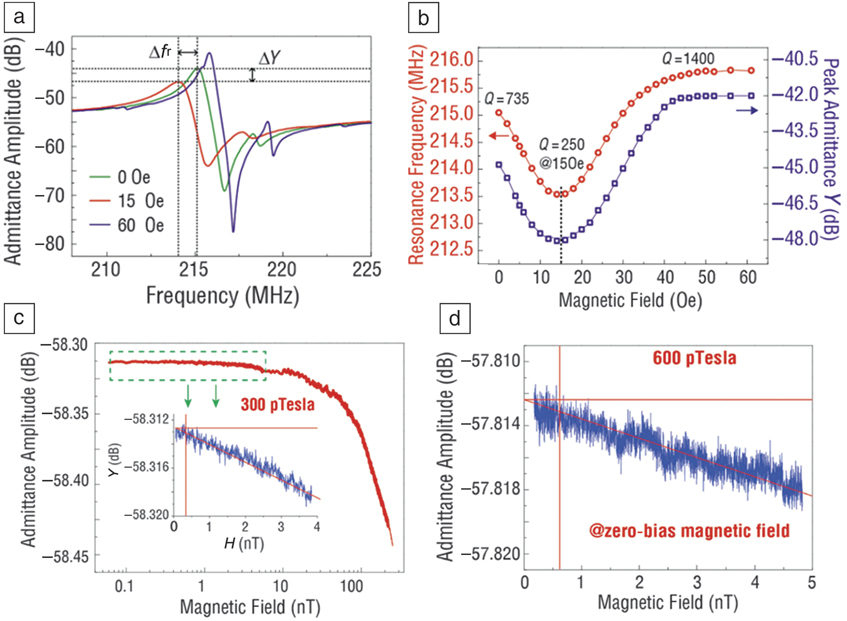
One open challenge has been in sensing weak DC and low-frequency alternating current (AC) magnetic fields. The DC magnetic field dependence of ME coupling can be used for DC magnetic field sensing. However, an AC magnetic field is needed to drive the ME sensors at a certain frequency for sensing the DC magnetic field using ME coupling.Reference Dong, Zhai, Li and Viehland17 The large power consumption for generating AC magnetic fields and comparatively low sensitivity make sensing DC magnetic fields for ME sensors challenging. NanReference Nan, Hui, Rinaldi and Sun18 demonstrated a self-biased NEMS ME sensor for application as a magnetometer that was based on piezomagnetic (FeGaB/Al2O3) multilayer nanoplate resonator at 215 MHz. The electromechanical resonance frequency change was attributed to the change in Young’s modulus, which was induced by the bias magnetic field in FeGaB, or the delta-E effect. In Figure 3a,Reference Nan, Hui, Rinaldi and Sun18 the sensitivity of this sensor can be observed from the admittance curve (the reciprocal of the impedance) versus the frequency at different DC bias magnetic fields (0 Oe, 15 Oe, and 60 Oe) applied along the length direction of the resonator, showing an electromechanical resonance frequency of 215 MHz at zero bias. Both resonance frequency, f r, and peak admittance amplitude, Y, at the resonance frequency exhibited similar trends with the DC bias magnetic field, as shown in Figure 3b, reaching minimum values at a bias field of 15 Oe. Both quantities then increase until the FeGaB/Al2O3 multilayer was saturated at 50∼60 Oe. The quality factor, Q, follows the same trend as the Young’s modulus, indicating that it may be strongly related to the magnetic anisotropy and magnetic domain wall. Under a high magnetic field, Q is largely enhanced, which could be due to the elimination of magnetic domain walls and a decrease in magnetic losses.
(a) Admittance curve of the nanoelectromechanical systems (NEMS) sensor at various bias direct current (DC) magnetic fields, showing an electromechanical resonance frequency of 215 MHz. (b) Resonance frequency and admittance amplitude at the resonance frequency as a function of DC magnetic field. Both resonance frequency, f r, and peak admittance amplitude, Y, exhibited similar trends with the DC bias magnetic field, which reaches minimum values at a bias field of 15 Oe. (c) The sensitivity and linearity of the DC magnetic field sensor with DC bias magnetic field of 5 Oe. The inset shows the zoomed-in part (green box) ranging from 50 pT to 4 nT in a magnetically unshielded environment. The red/orange/brown lines are for reference of linearity. The measurement value of the admittance amplitude starts to scatter at 300 pT, indicating the ultrasensitive magnetic sensor with a detection range starting from ∼300 pT. (d) Sensitivity and linearity of the DC magnetic field sensor at zero-bias magnetic field in a magnetically unshielded environment showing a limit of detection as low as 600 pT under the self-bias condition. The red/orange/brown lines are for reference of linearity. Note: H, magnetic field; Q, quality factor; pT, pTesla.Reference Nan, Hui, Rinaldi and Sun18

A fixed 5 Oe DC bias magnetic field was used to tune the magnetic materials to reach the maximum slope of the electromechanical resonance frequency versus magnetic field, as shown in Figure 3c. The inset in Figure 3c shows an enlarged view with the small DC magnetic field ranging from 50 pT to 4 nT. The measurement value of the admittance amplitude starts to scatter at 300 pT, indicating the detection range starts at ∼300 pT. The limit of detection as low as 600 pT is measured under the self-bias condition shown in Figure 3d, which is comparable to 300 pT results (Figure 1c inset). The integrated RF NEMS ME sensor is compact, power-efficient, and represents a new class of ultrasensitive magnetometers for DC and low-frequency AC magnetic fields.
Acoustically actuated NEMS ME antennas
One of the key challenges for state-of-the-art conventional antennas lies in their miniaturization. Conventional antennas rely on an electromagnetic wave resonance, and therefore, typically have a size of more than one-tenth of the electromagnetic wavelength, λ0. The limitation for antenna size miniaturization has made it challenging to achieve compact antennas and antenna arrays particularly at very high frequency (30–300 MHz) band and ultrahigh frequency (0.3–3 GHz) band. Antennas are basically an array of conductors that generate an oscillating electric field and magnetic field through an oscillating electric current, required to ensure a large radiation amplitude. However, there is another path to attain radiation power since electricity and magnetization are always coupled together, which indicates the magnetic current also generates an electromagnetic wave. Multiferroics have been studied for ME antennas for more than five years.Reference Yao and Wang19–Reference Domann and Carman23 Strong ME coupling, if realized dynamically at RFs in ME heterostructures, could enable voltage-induced RF magnetic currents that radiate electromagnetic waves and acoustically actuated nanoscale ME antennas with a new receiving and transmitting mechanism.Reference Nan, Lin, Gao, Matyushov, Yu, Chen, Sun, Wei, Wang, Li, Wang, Belkessam, Guo, Chen, Zhou, Qian, Hui, Rinaldi, McConney, Howe, Hu, Jones, Brown and Sun24
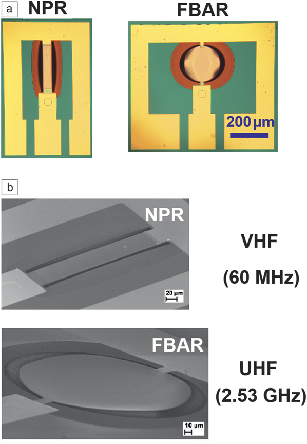
The antennas are based on a bulk acoustic wave resonator to transfer dynamic strain across the piezoelectric layer and magnetostrictive layer. Two proposed antennas shown in Figure 4, nanoplate resonators (NPRs) and FBARs,Reference Nan, Lin, Gao, Matyushov, Yu, Chen, Sun, Wei, Wang, Li, Wang, Belkessam, Guo, Chen, Zhou, Qian, Hui, Rinaldi, McConney, Howe, Hu, Jones, Brown and Sun24 have the same excitation, but have different resonance modes, providing a variety of frequency coverage. From the transmitting aspect, an RF electric field induces an alternating strain wave/acoustic wave that can induce a dynamic change in magnetization due to converse ME coupling and generate a magnetic current for radiation. Reciprocally, from the receiving aspect, the RF magnetic field component of the electromagnetic wave can be detected and induce a dynamic voltage/charge due to the direct ME coupling. The acoustic wavelength is approximately five orders shorter than the electromagnetic wavelength at the same frequency. Therefore, since the ME antennas are operating at the acoustic resonant frequency instead of the electromagnetic wave resonant frequency, the antennas can dramatically shrink to hundreds to thousands of times smaller dimensions.
(a) Optical images of the fabricated (left) nanoplate resonators (NPRs) and (right) thin-film bulk acoustic resonators (FBARs). (b) Scanning electron microscope image of the fabricated (top) NPRs and (bottom) FBARs. Note: VHF, very high frequency; UHF, ultrahigh frequency.

A ground plane is a flat or nearly flat horizontal conducting surface. The ground plane plays a major role in determining radiation characteristics, including gain. However, the imaging current, induced in the metal while a current passes, flowing in the opposite direction of the planar antennas, can cancel out the radiation from the antennas. This is why most large-profile antennas are in a vertical position and perpendicular to the surface, such as a vertical quarter-wave dipole, where the imaging current serves as part of the antenna for in-phase radiation. The ME antennas use magnetic currents for radiation instead of electric currents. The in-phase imaging current provides 3 dB gain enhancement while attaching to the ground. This ground-plane immunity property can enable a variety of applications on metallic surfaces and on the human body, which is also considered as a ground plane.
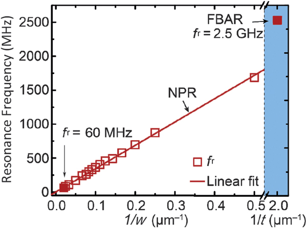
All antenna devices in this studyReference Nan, Lin, Gao, Matyushov, Yu, Chen, Sun, Wei, Wang, Li, Wang, Belkessam, Guo, Chen, Zhou, Qian, Hui, Rinaldi, McConney, Howe, Hu, Jones, Brown and Sun24 were fabricated with the same five-mask fabrication process on one small chip that includes thousands of antennas. The resonance frequency, f r, of various devices were measured with different design principles and geometries via a network analyzer. Figure 5 plots f as a function of 1/w (w = width) for NPRs and 1/t (t = thickness) for FBARs.Reference Nan, Lin, Gao, Matyushov, Yu, Chen, Sun, Wei, Wang, Li, Wang, Belkessam, Guo, Chen, Zhou, Qian, Hui, Rinaldi, McConney, Howe, Hu, Jones, Brown and Sun24 As shown, the f of NPR devices is inversely proportional to w for NPRs, and f is inversely proportional to the AlN thickness for FBAR. This indicates that the frequency of the antenna is simply defined by the resonator geometry. This indicates that by using a simple device geometry design, we can achieve a wide frequency band from tens of MHz to tens of GHz on only one chip. A bank of multifrequency MEMS resonators can be connected to a CMOS oscillator circuit for the realization of reconfigurable ME antenna arrays.
Measured resonance frequency, f r, as a function of 1/w (w is width) for nanoplate resonators (NPRs) and 1/t (t is thickness) for thin-film bulk acoustic resonators (FBARs) resonators. By using a simple device geometry design, we can achieve a wide frequency band from tens of MHz to tens of GHz on only one chip.Reference Nan, Lin, Gao, Matyushov, Yu, Chen, Sun, Wei, Wang, Li, Wang, Belkessam, Guo, Chen, Zhou, Qian, Hui, Rinaldi, McConney, Howe, Hu, Jones, Brown and Sun24

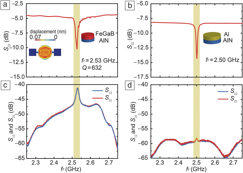
For antenna gain measurements, a calibrated linear polarization standard horn antenna and an ME antenna were connected to a vector network analysis device, which is an essential RF and microwave measurement tool. The resonance frequency was found to be 2.53 GHz by measuring the return loss (S 22), as shown in Figure 6a, with a peak return loss of 10.26 dB. In Figure 6b, a nonmagnetic control device with Al/AlN was also tested with the same experimental setup and at the same resonance frequency near 2.5 GHz. The control device exhibited a similar S 22 as the ME antenna, which indicates similar power is transferred into both antennas. The receiving and transmitting behavior of ME antennas corresponds to the S 21 and S 12 parameters, respectively, as shown in Figure 6c. The antenna gain for the ME antenna is calculated to be −18 dBi through the gain comparison method. However, as seen in Figure 6d, no clear resonance peak was observed in the control antenna measurements, which is ∼20 dB lower than the performance of ME antenna. The ME coupling effect likely dominates the performance of the antenna transmission.
(a) Return loss (S 22) of magnetoelectric thin-film bulk acoustic resonators (ME FBAR). The inset shows the simulated out-of-plane displacement of the circular disk at resonance peak position indicating the thickness direction resonance. (b) Return loss (S 22) curve of the nonmagnetic Al/AlN control FBAR. Both magnetic and nonmagnetic devices had similar return loss curves indicating that the same energy transferred into the both devices. (c) Transmitting and receiving behavior (S 12 and S 21, respectively) of the ME FBAR. (d) Transmitting and receiving behavior (S 12 and S 21, respectively) of the nonmagnetic Al/AlN control FBAR. The curves in the nonmagnetic device are ∼20 dB lower than the performance of those in the magnetic device. Therefore, we can suggest that the ME coupling effect dominates the performance of the antenna transmission.Reference Nan, Lin, Gao, Matyushov, Yu, Chen, Sun, Wei, Wang, Li, Wang, Belkessam, Guo, Chen, Zhou, Qian, Hui, Rinaldi, McConney, Howe, Hu, Jones, Brown and Sun24 Note: f r, resonance frequency; Q, quality factor.

Conclusion
Strong strain-mediated ME coupling in magnetic/ferroelectric heterostructures has attracted great interest and has been introduced with different integrated multiferroic devices, including novel integrated magnetic tunable inductors, dual H- and E-field tunable RF bandpass filters with nanomechanical ME resonators, novel RF nanomechanical ME resonators with pico-Tesla sensitivity for DC magnetic fields, and acoustically actuated NEMS ME antennas with one to two orders size reduction. These tunable multiferroic RF/microwave devices with the capability of being integrated to CMOS technology are compact, lightweight, and power efficient, and provide great opportunities for next-generation reconfigurable RF/microwave communication systems and radar, spintronics, sensing, biomedical applications, Internet of Things, and other applications.
Acknowledgments
This work was supported by DARPA through Award D15PC00009, the W.M. Keck Foundation, the NSF TANMS ERC Award 1160504, and in part by the AFRL through Contract FA8650–14-C-5706. Microfabrication was performed in the George J. Kostas Nanoscale Technology and Manufacturing Research Center.

Hwaider Lin has been a research associate at the NSF ERC Center for Translational Applications of Nanoscale Multiferroic Systems. He received his PhD degree in electrical and computer engineering from Northeastern University in 2018. His research focuses on magnetoelectric antennas for radio-frequency, microwave, and biomedical applications. He has given more than 25 presentations at international conferences and has published more than 30 research papers. His academic awards include the NASA Tech Briefs Design Contest–First Prize, in 2018, the ECE Department Distinguished Research Assistant Award and the Northeastern University Outstanding Graduate Student Award. Lin can be reached by email at lin.hw@husky.neu.edu.

Michael R. Page is a research physicist in the Functional Materials Division, Materials and Manufacturing Directorate, Air Force Research Laboratory, Air Force Materiel Command, at the Wright-Patterson Air Force Base. He performs research in the area of defect centers for quantum information applications and magnetic materials for agile resonance frequency devices. He is currently focusing on developing nitrogen vacancy centers in single-crystal diamond as a solid-state materials platform for quantum information and magnetic sensing. Page can be reached by email at michael.page.16@us.af.mil.

Michael E. McConney is a materials scientist in the Functional Materials Division, Materials and Manufacturing Directorate at the Air Force Research Laboratory. He is active in optics, photonics, and novel anisotropic materials, including multiferroic materials. He has published 40 manuscripts, and his work has been cited more than 2000 times. He is an expert in the mechanics and optics of anisotropic materials and thin-film physics. McConney can be reached by email at michael.mcconney.1@us.af.mil.

John G. Jones is a senior materials research engineer at the Air Force Research Laboratory in the Nanoelectronics Materials Branch of the Materials and Manufacturing Directorate. He received his BS EE degree from Rose-Hulman Institute of Technology in 1991 and his PhD degree from the University of Cincinnati in 1997. His research interests focus on nanoelectronic thin-film materials process development utilizing physical vapor deposition, in situ ellipsometry for closed-loop feedback, and engineering second-order nonlinear optical materials. Jones can be reached by email at john.jones.66@us.af.mil.

Brandon M. Howe is a material engineer at the Air Force Research Laboratory (AFRL) Materials and Manufacturing Directorate, Nanoelectronic Materials Branch. He joined the AFRL under the Science, Mathematics, and Research for Transformation Scholar Program in 2006. He earned his PhD degree in materials science in 2011 from the University of Illinois at Urbana-Champaign. During this time, he received several awards in the area of epitaxial thin-film growth and vacuum technology. His research focuses on renovating, redesigning, and constructing an ultrahigh vacuum pulsed laser deposition and magnetron sputter epitaxy suite. He leads an electronic materials development effort focused on multifunctional and semiconducting oxides for next-generation tunable radio-frequency/microwave components and power conversion. Howe can be reached by email at brandon.howe.6@us.af.mil.

Nian Sun is the founder and chief technical advisor of Winchester Technologies, LLC, and professor in the Electrical and Computer Engineering Department, and Director of the W.M. Keck Laboratory for Integrated Ferroics at Northeastern University. He received his PhD degree from Stanford University. He is an editor of the journals Sensors and IEEE Transactions on Magnetics. He is a Fellow of the Institute of Physics and the Institution of Engineering and Technology. Prior to joining Northeastern University, he was a scientist at IBM and Hitachi Global Storage Technologies. He was the recipient of the NSF CAREER Award, ONR Young Investigator Award, and the Søren Buus Outstanding Research Award. He has more than 240 publications and more than 20 patents and patent applications. Sun can be reached by email at n.sun@northeastern.edu.