
I. INTRODUCTION
A. Background
We begin by exploring the origin of piezoelectricity in non-nitride III–V nanowires (NWs) (referred to simply as III–V NWs from here onwards). The piezoelectric effect arises as a result of an applied stress causing a relative displacement of ions or polar components within a piezoelectric material, resulting in a change in net polarisation. Piezoelectricity thus refers to the linear interaction between the mechanical and the electrical states of certain materials where the stress and strain are interrelated with the resulting electric displacement induced in the material. Among the 32 crystal classes, 11 are centrosymmetric and nonpolar such that an applied stress results in symmetrical ionic displacement and no net dipole moment. Of the 21 noncentrosymmetric classes, 20 are piezoelectric with the exception being the 432 cubic system. Piezoelectricity manifests as both the direct piezoelectric effect, where a polarisation is created in response to an applied stress, and the converse piezoelectric effect, where an applied electric field creates a strain within the material. The effect can be described mathematically with a set of complimentary equations given below:
 $$D = {\varepsilon _{\rm{T}}}E + {\rm{d}}T\quad ,$$
 $$S = {{\rm{d}}^t}E + {s_{\rm{E}}}T\quad .$$
Here, T and S represent stress and strain, respectively, which are second rank tensors related to an applied force and the normal to the area over which it acts. D and E represent the electric displacement and electric field which are vectors. εT is the dielectric permittivity of the material at constant stress, d is the piezoelectric tensor, and s E is the elastic compliance at constant electric field. These three terms are represented by second, third, and fourth rank tensors, respectively, where d t is the transpose of d. Voigt notation is commonly used to simplify the tensors since static equilibrium requires T ij = T ji , S ij = S ji , and s ijkl = s ijlk = s jikl = s jilk , and further simplifications may arise when the ε, d, and s tensors have symmetries for certain directions. Bulk III–V semiconductor materials with the noncentrosymmetric zinc blende (ZB) crystal structure possess off-diagonal “shear” piezoelectric components, while III–V NWs of the same material, that more likely crystalize in the wurtzite (WZ) crystal structure, exhibit distinct axial piezoelectric components. Reference Calahorra, Guan, Halder, Smith, Cohen, Ritter, Penuelas and Kar-Narayan1 III–V semiconductors therefore present an interesting material system in which to investigate and possibly manipulate piezoelectricity, based on a combination of dimensionality, geometry, and crystal structure.
The past decade has seen a fast-growing scientific interest in piezoelectric applications based on nanomaterials, particularly following the pioneering work from Wang’s group regarding ZnO NWs and nanoribbons, Reference Zhao, Wang and Mao2–Reference Wang, Zhou, Song, Liu, Xu and Wang4 and their applications in mechanical energy harvesting. Piezoelectricity in II–VI materials such as ZnO and III-Ns is well documented, Reference Bernardini, Fiorentini and Vanderbilt5,Reference Goniakowski, Finocchi and Noguera6 and accordingly, significant research efforts have been directed toward understanding and utilizing piezoelectricity in NWs of these materials. Reference Zhao, Wang and Mao2,Reference Wang, Zhou, Song, Liu, Xu and Wang4,Reference Nam, Jaroenapibal, Tham, Luzzi, Evoy and Fischer7–Reference Jamond, Chretien, Houze, Lu, Largeau, Maugain, Travers, Harmand, Glas, Lefeuvre, Tchernycheva and Gogneau10 GaN NWs Reference Minary-Jolandan, Bernal, Kujanishvili, Parpoil and Espinosa8 and ZnO nanobelts Reference Zhao, Wang and Mao2 have been examined via piezoresponse force microscopy (PFM) and were found to have an increased piezoelectric response as compared to the bulk, possibly due to reduced mechanical constraints. Single NWs as well as NW ensembles have been used to realize mechanical energy harvesting devices, as well as piezocontrolled diodes and transistors. Reference Wang and Song3,Reference Wang, Zhou, Song, Liu, Xu and Wang4,Reference Jamond, Chretien, Houze, Lu, Largeau, Maugain, Travers, Harmand, Glas, Lefeuvre, Tchernycheva and Gogneau10–Reference Wang12 Notably, the term “piezotronic” was coined to describe the unique effects arising when semiconductor junctions (Schottky or p–n) are subject to strain. Reference Wang11–Reference Wen, Wu, Pan, Hu, Yang and Wang15
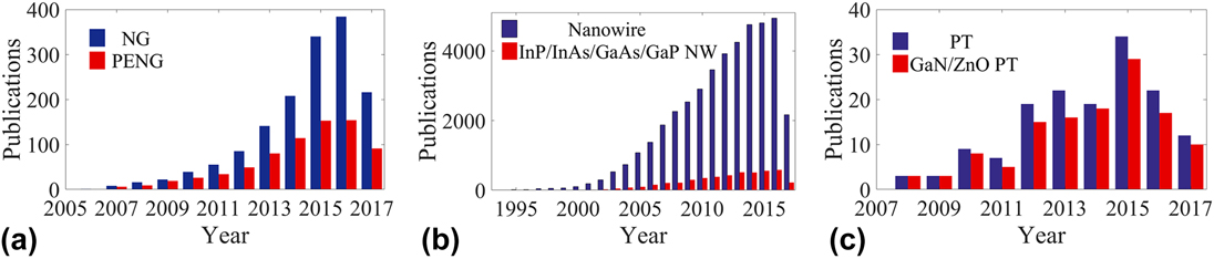
Figure 1(a) shows the annual number of publications revolving around the topic of “Nanogenerator” and “Piezoelectric Nanogenerator” which concerns the ability to harvest ambient mechanical energy and transform it to useful electrical energy. Indeed, about 50% of publications revolving around this topic deal with piezoelectric properties at the nanoscale. The interest in nanoscale materials is older than that, with NWs (having diameters of several nanometres to a few hundred nanometres) having been widely studied. Reference Dasgupta, Sun, Liu, Brittman, Andrews, Lim, Gao, Yan and Yang16–Reference Krogstrup, Jorgensen, Heiss, Demichel, Holm, Aagesen, Nygard and Morral18 III–V semiconductor NWs are at the focus of about 15% of related publications, as seen in Fig. 1(b) showing publications revolving around the topic of “Nanowires” and (a few non-nitride) “III–V Nanowires”.
Web of Science topical publication data: (a) “Nanogenerator” versus “Piezoelectric + Nanogenerator”; (b) “Nanowire” versus “InP + Nanowire OR InAs + Nanowire OR GaAs + Nanowire OR GaP + Nanowire”; and (c) “Piezotronic” versus “Piezotronic + GaN OR Piezotronic + ZnO”.

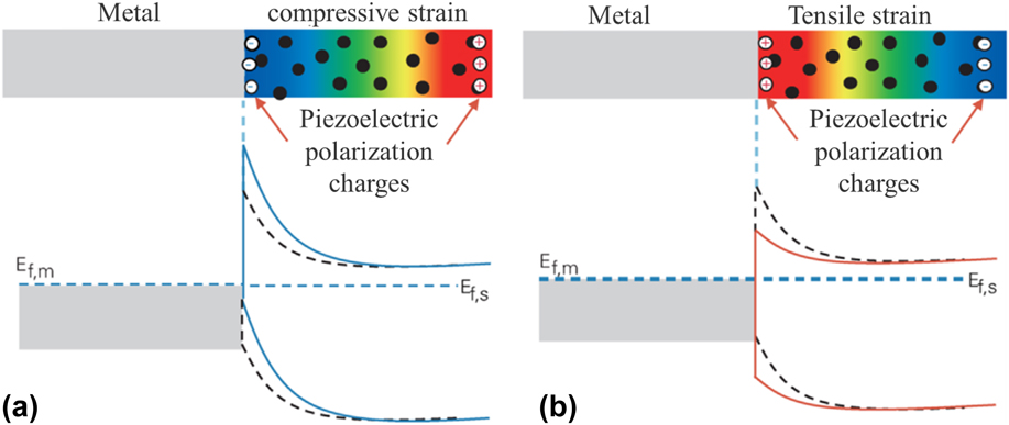
In addition to energy harvesting, traditional applications of piezoelectric materials, such as sensing applications, have been widely studied in ZnO- and GaN-based nanomaterials. Reference Wang, Zhou, Song, Liu, Xu and Wang4,Reference Wang11,Reference Zhou, Gu, Fei, Mai, Gao, Yang, Bao and Wang13 Considering the electrical and optical properties of semiconductors, the terms “piezotronics” and “piezophototronics” have been coined to, respectively, describe the electromechanical and opto–electromechanical interactions taking place in piezoelectric semiconductor junction-based devices. This is an emerging research field with many potential sensing and energy-based applications, which is currently based on a handful of candidate material systems. Further development of the field would require investigation and development of a wide range of piezoelectric semiconductors, including III–V materials which exhibit a wider range of band gaps and mechanical properties that may be appropriate for specific applications. A schematic of the metal-piezoelectric semiconductor piezotronic effect is shown in Fig. 2. Briefly, when a depleted piezoelectric semiconducting region experiences stress, a negative or positive piezopotential (dependent upon the crystal orientation and the sign of the resulting strain) will result in additional interface charge. This charge is not neutralized, considering that the material is depleted of charge carriers and therefore serves to modify the Schottky barrier height. Taking into account the optoelectronic properties of Schottky junctions, the piezophototronic effect relates to such junctions when light is shone upon them. To elucidate piezoelectric semiconductor related research, Fig. 1(c) shows the annual number of publications revolving around “piezotronic” and “GaN/ZnO piezotronic”. Indeed, GaN- and ZnO-related publications comprise the majority of papers, while non-nitride III–V nanomaterials have hardly been studied in the context of piezotronics. In fact, a Web of Science topical search of “InP/GaAs/InAs/GaP piezotronic” yields only 5 results—none of which actually deal with III–V materials.
Schematic describing the piezotronic effect: (a) and (b) show a piezoelectric semiconductor in contact with a metal, such that compression (a) and tension (b) of the semiconductor give rise to uncompensated surface charge at the Schottky interface—modulating the barrier height. Reprinted with permission from Elsevier. Reference Wen, Wu, Pan, Hu, Yang and Wang15

The relative lack of interest in III–V NW piezoelectricity is intriguing, considering the closeness in applications as well as in underlying physics of III–Vs and III-Ns. Reference Singh19,Reference Wood and Jena20 One possible reason for this might be the smaller piezoelectric coefficients associated with non-nitride III–V materials. Reference Singh19,Reference Wood and Jena20 However, these are not orders of magnitude apart (∼5 pm/V for III-Ns, ∼1 pm/V for III–Vs), and moreover, with the reported increase in effective piezoelectric coefficients in NWs as compared to bulk, Reference Minary-Jolandan, Bernal, Kujanishvili, Parpoil and Espinosa8 research into III–V NW piezoelectric properties and applications may be of considerable interest. Another reason why piezoelectric properties of III–V NWs have been rarely studied may be due to the predisposition of the III–V community toward pure electronic and optical applications as well as the inherited knowledge from the vast world of III–V bulk and epitaxial thin films. Here, the dominant crystal growth orientation is <100> (e.g., see Ref. Reference Hayakawa, Kondo, Suyama, Takahashi, Yamamoto and Hijikata21), and the dominant crystal structure for III–V materials is ZB, where spontaneous electrical polarization is negligible, and piezoelectricity is limited to three shear coefficients. Reference Singh19 Therefore, although known, recognized, and used to some extent for micro-electromechanical systems, Reference Nedbal and Klier22,Reference Klier and Nedbal23 polarization and piezoelectricity do not play a significant role in traditional III–V technology. This stands in striking contrast to GaN technology where the dominant crystal structure is WZ; a considerable degree of spontaneous electrical polarization exists, and the dominant growth orientation is actually the polar <0001> (equivalent to <111> in ZB structure). For example, GaN high-electron mobility transistor technology is physically based on the spontaneous and piezoelectric polarization mismatch related to III-N heterostructures. Reference Wood and Jena20 Hence, there has been understandably more awareness and interest in nanoscale semiconductor piezoelectricity from the III-N scientific community than from the III–V community. However, as we will explain in the first few sections of this review, III–V NWs have a lot in common with the III-N point-of-view when it comes to piezoelectricity, and in light of the growing interest in semiconductor piezo-electronics and the vast interest in III–V NWs, there exists tremendous scope to explore and exploit the piezoelectric properties of III–V NWs.
This review is structured as follows: in the remainder of Sec. I, we briefly review piezoelectricity and related applications in bulk III–V materials, as well as the key distinctions between III–V bulk and NWs in terms of crystalline structure. In Sec. II, we review the current status of NW mechanical properties, with emphasis on studies dedicated to WZ III–V NWs. In Sec. III, we review the body of work related to piezoelectric and electromechanical effects in III–V NWs, considering three aspects: piezoelectricity related to internal stresses, piezoelectricity related to external mechanical forces, and finally direct observations of fundamental piezoelectricity in III–V NWs. In Sec. IV, we conclude and point out the challenges lying ahead in this research direction. The review considers both theoretical and experimental results, and therefore when relevant, comparisons made between experiments and theory will be discussed. However, while some of the experimental setups and results will be examined and compared, a thorough discussion of theoretical methods for calculating mechanical/piezoelectric properties and related intricacies are outside the scope of this review.
B. Piezoelectricity in bulk III–V materials
Although not playing a significant role in the design and analysis of electronic devices, piezoelectricity arising from the noncentrosymmetric ZB structure in III–V semiconductors has been long known. Reference Hanada, Yao and Hong24,Reference Lawaetz25 III–V materials exhibit shear piezoelectricity (relative to the basic cubic cell vectors), with an identical value for all three orientations [see Eq. (1)]. This property has been utilized to demonstrate electromechanical applications. Reference Nedbal and Klier22,Reference Klier and Nedbal23,Reference Huang, Cheng, Zhou, Pesala, Chang-Hasnain and Pisano26,Reference Hjort, Soderkvist and Schweitz27 Furthermore, the effect of internal piezoelectric fields on the performance of <111>-oriented electronic devices has been considered. Reference Hernandez, Izpura, Calleja and Munoz28,Reference Campbell, Joswick, Smith and Miles29
Notably, some early studies which are closely related to current piezoelectric NW studies have gone relatively unnoticed. Two interesting studies are those by Kasuka et al. which represent an early demonstration of the piezotronic effect (albeit, prior to coining the term) on both p-type and n-type <111>-oriented GaP Schottky diodes. Reference Kusaka30,Reference Kusaka, Hiraoka, Hirai and Okazaki31 In these two papers, Kasuka and coworkers have shown that the effect of <111>- oriented strain on the Schottky barrier height is sensitive both to carrier polarity (electrons/holes) as well as crystal face (Ga/P) contacting the metal. Furthermore, as would be expected, in the case of compression, the trends were mirrored. An electromechanical analytical analysis (considering stress, electrical displacement, and Poisson’s equation) provided an inversely linear relation between the barrier height and the strain. Bearing in mind that for diodes, the current is exponentially dependent on barrier height, this has implications for the strain-sensitivity of the piezotronic effect. It is worth revisiting Fig. 2 to qualitatively understand these effects. Figures 2(a) and 2(b) show an n-type Schottky contact subjected to compressive and tensile stresses, correspondingly. These stresses result in opposite polarization charges at the interface, hence the opposite effect on the barrier and current. The semiconductor polarity will also have a similar effect: while for n-type band bending upwards (compression in this example) results in increase of the barrier, for p-type (of the same polarity), the same mechanical input will decreases the barrier.
In a recent work, seeking to develop magnetoelectric composites, Gerngross et al. have examined the piezoelectric properties of porous InP substrates (ZB), obtained by chemical etching. Reference Gerngross, Sprincean, Leisner, Carstensen, Foll and Tiginyanu32 Interestingly, they found that the piezoelectric strain coefficient (measured optically) was up to 30 times larger than the literature value, depending on the details of the etching process. They attributed the effect to reduced free-carrier screening of the piezogenerated voltage, arising from increased surface-related depletion of the porous structure. We further suggest that in addition to depletion, the porous material is softer, giving rise to further enhancement to the measured coefficient, similar to reports for enhanced mechano-electric coupling in porous PVDF (polyvinylidene fluoride). Reference Cha, Kim, Kim, Ku, Sohn, Park, Song, Jung, Lee, Choi, Park, Wang, Kim and Kim33
If so, we have seen in the above that piezoelectricity in III–Vs have in fact been considered in the past and examined both experimentally and theoretically in different ways for various applications. Nevertheless, this trend has not been widely followed; the main reason probably being the tendency to prefer the <110> and <100> planar growth directions over the polar <111> direction, due to practical difficulties associated with the growth of thin films. In sharp contrast, <111> orientations are the default working environment for III–V NWs, as discussed below, and this should motivate revisiting this aspect of III–Vs and its relevance to piezoelectricity when considering NWs.
C. The effect of growth orientation and crystal structure on III–V NW piezoelectricity
III–V NWs may be realized by either bottom-up or top-down approaches. Although top-down NWs may represent the next generation of electronic devices, Reference Cutaia, Moselund, Schmid, Borg, Olziersky and Riel34,Reference Gu, Koybasi, Wu and Ye35 bottom-up NWs introduce interesting physical phenomena due to the realization using crystal growth methods. Reference Dasgupta, Sun, Liu, Brittman, Andrews, Lim, Gao, Yan and Yang16,Reference Fortuna and Li36,Reference Dick, Caroff, Bolinsson, Messing, Johansson, Deppert, Wallenberg and Samuelson37 Bottom-up III–V NWs are usually grown using a nanosized metal catalyst lying on the growth substrate, which can be either silicon or a bulk III–V substrate. Reference Fortuna and Li36,Reference Dick and Caroff38 NWs can also be grown using catalyst-free methods, where a nanosized pore within a growth-selective mask facilitates the growth of a NW. Reference Noborisaka, Motohisa and Fukui39 A few intermediate methods exist, combining characteristics of both; these include self-catalysed grown NWs, where inside the pore, a nonforeign metallic particle catalyses the growth (usually group-III metal), Reference Colombo, Spirkoska, Frimmer, Abstreiter and Morral40 and catalyst-assisted selective-area NW growth, where the metal catalyst is deposited within a pore in a selective area mask. Reference Dalacu, Kam, Austing, Wu, Lapointe, Aers and Poole41,Reference Kelrich, Calahorra, Greenberg, Gavrilov, Cohen and Ritter42
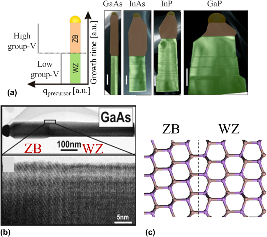
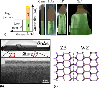
Although many unique properties arise from the various growth regimes, Reference Mohan, Motohisa and Fukui43–Reference Calahorra, Kelrich, Cohen and Ritter46 there are common traits to all: due to energy considerations, cubic III–V NWs are most likely grown axially in the <111> (ZB) orientation. Reference Fortuna and Li36 Consequently, the majority of III–V NW related studies are based on {111} substrates (either III–V or silicon), whereby NWs are vertically grown on these surfaces. Furthermore, there is an increased probability for NW growth in the WZ crystalline structure, Reference Fortuna and Li36,Reference Lehmann, Wallentin, Jacobsson, Deppert and Dick44,Reference Joyce, Wong-Leung, Gao, Tan and Jagadish47–Reference Spirkoska, Arbiol, Gustafsson, Conesa-Boj, Glas, Zardo, Heigoldt, Gass, Bleloch, Estrade, Kaniber, Rossler, Peiro, Morante, Abstreiter, Samuelson and Morral49 in the <0001> orientation, also vertically aligned on {111} growth substrates. As will be seen below, both these characteristics indicate that studying piezoelectric properties of III–V NWs might be beneficial. Figure 3(a) shows an example of sharp crystal phase heterostructures in various III–V NWs. Reference Lehmann, Wallentin, Jacobsson, Deppert and Dick44 Next, an abrupt heterostructure is shown both experimentally [Fig. 3(b), single GaAs NW TEM], and schematically [Fig. 3(c)].
Crystal phase control in III–V NWs: (a) switching from WZ to ZB by increasing growth precursor flow for GaAs, InAs, InP, and GaP. Reprinted with permission from ACS Reference Lehmann, Wallentin, Jacobsson, Deppert and Dick44 ; (b) High resolution transmission electron microscopy (HR-TEM) image showing the phase purity around the GaAs crystal phase interface. Reprinted with permission from ACS Reference Lehmann, Wallentin, Jacobsson, Deppert and Dick44 ; and (c) schematic corresponding to the interface in (c).

As mentioned earlier, ZB III–V materials exhibit only shear piezoelectricity, rendering the piezoelectric strain tensor (using Voigt notation) Reference Singh19
 $${d_{{\rm{ZB}},\left[ {001} \right] }} = \left( {\matrix{ 0 \hfill & 0 \hfill & 0 \hfill & {{d_{14}}} \hfill & 0 \hfill & 0 \hfill \cr 0 \hfill & 0 \hfill & 0 \hfill & 0 \hfill & {{d_{14}}} \hfill & 0 \hfill \cr 0 \hfill & 0 \hfill & 0 \hfill & 0 \hfill & 0 \hfill & {{d_{14}}} \hfill \cr} } \right)\quad ,$$
where d 14 is a shear piezoelectric coefficient. The piezoelectric effect and tensor notations have been widely discussed in the literature, for example, see Ref. Reference Moheimani and Fleming50.
In NWs, where the dominant axial orientation is <111>, it is beneficial to rotate the tensor such that the piezoelectric axes correspond with sample geometry.
Reference Calahorra, Guan, Halder, Smith, Cohen, Ritter, Penuelas and Kar-Narayan1,Reference Boxberg, Sondergaard and Xu51,Reference Mengistu and Garcia-Cristobal52
Additionally, to chemically conform with WZ,
Reference Park and Chuang53
we choose the 3-axis to be [111], corresponding to [0001] in WZ, the 1-axis to be
 $\left[ {11\bar{2}} \right]$
, and 2-axis to be
 $\left[ {\bar{1}10} \right]$
(corresponding to
 $\left[ {10\bar{1}0} \right]$
and
 $\left[ {\bar{1}2\bar{1}0} \right]$
in WZ, respectively). The resulting matrix is
Reference Calahorra, Guan, Halder, Smith, Cohen, Ritter, Penuelas and Kar-Narayan1
 $${d_{{\rm{ZB}},\left[ {111} \right] }} = \left( {\matrix{ {{d_{11}}} \hfill & { - {d_{11}}} \hfill & 0 \hfill & 0 \hfill & {{d_{15}}} \hfill & 0 \hfill \cr 0 \hfill & 0 \hfill & 0 \hfill & {{d_{15}}} \hfill & 0 \hfill & {{d_{26}}} \hfill \cr {{d_{31}}} \hfill & {{d_{31}}} \hfill & {{d_{33}}} \hfill & 0 \hfill & 0 \hfill & 0 \hfill \cr} } \right)\quad .$$
The values of the coefficients are then
 $- {d_{15}} = {d_{33}} = \sqrt {{1 \over 3}} \widetilde {{d_{14}}}$
,
 ${d_{31}} = {1 \over 2}{d_{15}}$
,
 ${d_{11}} = - \sqrt {{1 \over 6}} \widetilde {{d_{14}}}$
, and
 ${d_{26}} = \sqrt {{2 \over 3}} \widetilde {{d_{14}}}$
, where
 $\widetilde {{d_{14}}}$
is the shear value from the original tensor [Eq. (3)].
In other cases, NWs crystallize in the WZ structure with <0001> axial orientation, and the piezoelectric matrix is
 $${d_{{\rm{WZ}},\left[ {0001} \right] }} = \left( {\matrix{ 0 \hfill & 0 \hfill & 0 \hfill & 0 \hfill & {{d_{15}}} \hfill & 0 \hfill \cr 0 \hfill & 0 \hfill & 0 \hfill & {{d_{15}}} \hfill & 0 \hfill & 0 \hfill \cr {{d_{31}}} \hfill & {{d_{31}}} \hfill & {{d_{33}}} \hfill & 0 \hfill & 0 \hfill & 0 \hfill \cr} } \right)\quad .$$
As evidenced above, in their most common forms, III–V NWs are expected to exhibit distinct piezoelectricity compared to bulk, due to geometry, crystal orientation, and crystal structure.
We list in Table I characteristic piezoelectric strain coefficients for a few III–V materials, GaN and ZnO. Note that while the ZB values are experimentally verified, the WZ values for III–Vs are theoretical, obtained using ab-initio calculations (AI)
Reference Al-Zahrani, Pal, Migliorato, Tse and Yu54
or by applying a quasi-cubic (QC) model, yielding
 ${e_{14,{\rm{ZB}}}} = \sqrt {{1 \over 3}} {e_{33,{\rm{WZ}}}}$
Reference Lawaetz25
and
 ${e_{31}} = - {1 \over 2}{e_{33}}$
.
Reference Berlincourt, Shiozawa and Jaffe55
The relations between piezoelectric charge coefficients (e
ij
) and piezoelectric strain coefficients (d
ij
) follow
Reference Hanada, Yao and Hong24
e
14 = d
14
c
44 for ZB, and
 $$\eqalign{ & {e_{31}} = {d_{31}}\left( {{c_{11}} + {c_{12}}} \right) + {d_{33}}{c_{13}} \cr & {e_{33}} = 2{d_{31}}{c_{13}} + {d_{33}}{c_{33}}\quad , \cr}$$
where c ij are stiffness coefficients. Reference Wang and Ye56 e ij coefficients are in C/m2; d ij coefficients are in pm/V.
The piezoelectric coefficients of III–V materials for ZB 〈111〉 orientation and for WZ.

If so, we can see that the theoretical predictions for the piezoelectric coefficients in WZ structure vary greatly [Table I]. Since all of these NWs are routinely grown, it should be possible to experimentally measure these quantities, validating existing theories and shedding light on possible applications. Notice that e ij and d ij coefficients do not necessarily follow similar trends; this is due to their co-relation incorporating the stiffness of the material.
II. MECHANICAL PROPERTIES OF WZ III–Vs
The interest in III–V NWs ushered the emergence of WZ III–V materials. The immediate implication was that the most basic physical properties became an interesting research topic both theoretically and experimentally. Surprisingly, the mechanical properties of WZ III–V NWs received little attention, compared to the vast interest in their optical properties Reference Duan, Huang, Cui, Wang and Lieber17,Reference Krogstrup, Jorgensen, Heiss, Demichel, Holm, Aagesen, Nygard and Morral18,Reference Yan, Gargas and Yang57 or the general interest in NW mechanical properties. Reference Calahorra, Shtempluck, Kotchetkov and Yaish58,Reference Heidelberg, Ngo, Wu, Phillips, Sharma, Kamins, Sader and Boland59 Nevertheless, in recent years, researchers have begun directly looking into this topic, either by applying nanomechanical methods using atomic force microscopy (AFM), Reference Dunaevskiy, Geydt, Lahderanta, Alekseev, Haggren, Kakko, Jiang and Lipsanen60,Reference Alekseev, Dunaevskii, Stovpyaga, Lepsa and Titkov61 in situ transmission electron microscopy (TEM) setups, Reference Wang, Wang, Joyce, Gao, Liao, Mai, Tan, Zou, Ringer, Gao and Jagadish62–Reference Chen, Burgess, An, Mai, Tan, Zou, Ringer, Jagadish and Liao64 or optical methods. Reference Mante, Lehmann, Anttu, Dick and Yartsev65
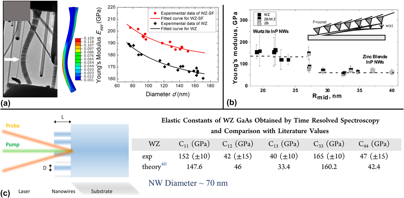
Figure 4 shows the results of mechanical characterization of WZ GaAs and InP NWs, obtained by the various methods mentioned above. Figure 4(a) shows the Young’s modulus obtained by Chen et al. by buckling tests (see inset) conducted on pure WZ and mixed phase GaAs NWs as reported in Ref. Reference Chen, Burgess, An, Mai, Tan, Zou, Ringer, Jagadish and Liao64; similar measurements have been conducted for ZB NWs as well. Reference Wang, Wang, Joyce, Gao, Liao, Mai, Tan, Zou, Ringer, Gao and Jagadish62 In both cases, a significant increase in the elastic modulus with decreasing diameter is found, and these findings were explained by the elastic core–shell model, where the GaAs native oxide exhibits a high elastic modulus, shifting the composite effective value upwards with size reduction. An additional result of this study was that the presence of stacking faults was associated with an additional increase in Young’s modulus [red and black curves in Fig. 4(a)]. In other studies, using optical measurements of WZ (and ZB) GaAs [Fig. 4(c)], Reference Mante, Lehmann, Anttu, Dick and Yartsev65 as well is in AFM-based nanoindentation measurements of WZ InP NWs [Fig. 4(b)], Reference Dunaevskiy, Geydt, Lahderanta, Alekseev, Haggren, Kakko, Jiang and Lipsanen60 the values obtained for WZ NWs were very close to theoretical predictions Reference Wang and Ye56,Reference Martin66 ; this was the case even for NWs thinner than those shown in the TEM-based studies. By further contrast, in the AFM-based study, stacking faults were associated with a considerable reduction of extracted modulus value and not an increase.
Experimentally obtained elastic modulus values for WZ GaAs and InP NWs. (a) TEM and finite-element analogue for compression of GaAs NWs (left) and axial Young’s modulus results for NWs w/wo stacking faults (right). Reprinted with permission from ACS Reference Chen, Burgess, An, Mai, Tan, Zou, Ringer, Jagadish and Liao64 ; (b) schematic of inclined InP NW bending (inset) and axial Young’s modulus results for NW w/wo stacking faults. Reprinted with permission from ACS Reference Dunaevskiy, Geydt, Lahderanta, Alekseev, Haggren, Kakko, Jiang and Lipsanen60 ; and (c) schematic of the optical pump-probe setup (left) and extracted versus theoretical stiffness coefficients for WZ GaAs NWs. Reprinted with permission from ACS. Reference Mante, Lehmann, Anttu, Dick and Yartsev65

Note that while both the AFM-based and optical studies took into account the inherent anisotropy of the elastic properties of III–V materials, the TEM-based studies did not and thus have possibly induced misinterpretation of the results during modeling. Furthermore, the role of the native oxide in increasing the effective modulus with diameter reduction requires further validation, e.g., by studies of NW with an enhanced oxide layer or with no oxide layer. Reference Calahorra, Shtempluck, Kotchetkov and Yaish58 Indeed, in different studies, researchers have correlated stacking faults and surface oxide with a reduced Young’s modulus (as compared to theoretical values) of WZ and mixed phase InAs NWs. Reference Li, Wei, Xu, Ning, Shu, Wang, Pan, Zhao, Yang and Chen67,Reference Erdelyi, Madsen, Safran, Hajnal, Lukacs, Fulop, Csonka, Nygard and Volk68
While there is a definite need for further study of the basic mechanical properties of III–V NWs and, in particular, the role of stacking faults, it seems that for NWs thicker than a few nanometres, the current theories provide an adequate basis for the assessment of the compliance/stiffness tensor and the subsequent elastic modulus, which represents a fundamental requirement for the analysis of piezoelectricity. Reference Wang and Ye56
III. ELECTROMECHANICAL EFFECTS IN III–V NWs
Various researchers have considered the piezoelectric properties of III–V materials in forming NWs and NW heterostructures. The chronological advance of these studies shows earlier focus on effects resulting from internal strains in nanoheterostructures, moving on to examination of the effect of external mechanical manipulation on optical or electrical properties, and finally studies focusing on the core piezoelectric effect in III–V NWs.
A. Electromechanical effects related to internal strain
Several studies have calculated the effects of strain resulting from III–V NW heterostructures on their properties, with consideration of the piezoelectric effect in particular, Reference Boxberg, Sondergaard and Xu51,Reference Mengistu and Garcia-Cristobal52,Reference Al-Zahrani, Pal, Migliorato, Tse and Yu54,Reference Niquet and Mojica69,Reference Faria and Sipahi70 with earlier studies having considered similar effects in planar quantum dots. Reference Holm, Pistol and Pryor71,Reference Bester and Zunger72 Niquet and Mojica have performed band diagram calculations for InAs segments in InP NWs (and vice versa). Reference Niquet and Mojica69 Interestingly, such earlier studies considered ZB NWs, while more recent studies have started considering WZ as well. Faria Junior and Sipahi have calculated the band structures of the WZ/ZB InP NW heterostructure, with consideration of spontaneous and piezoelectric polarization. Reference Faria and Sipahi70 Additional studies considering core–shell, embedded, or periodic heterostructures where crystal orientation and structure affect piezoelectric potential have been published as well. Reference Boxberg, Sondergaard and Xu51,Reference Mengistu and Garcia-Cristobal52,Reference Al-Zahrani, Pal, Migliorato, Tse and Yu54
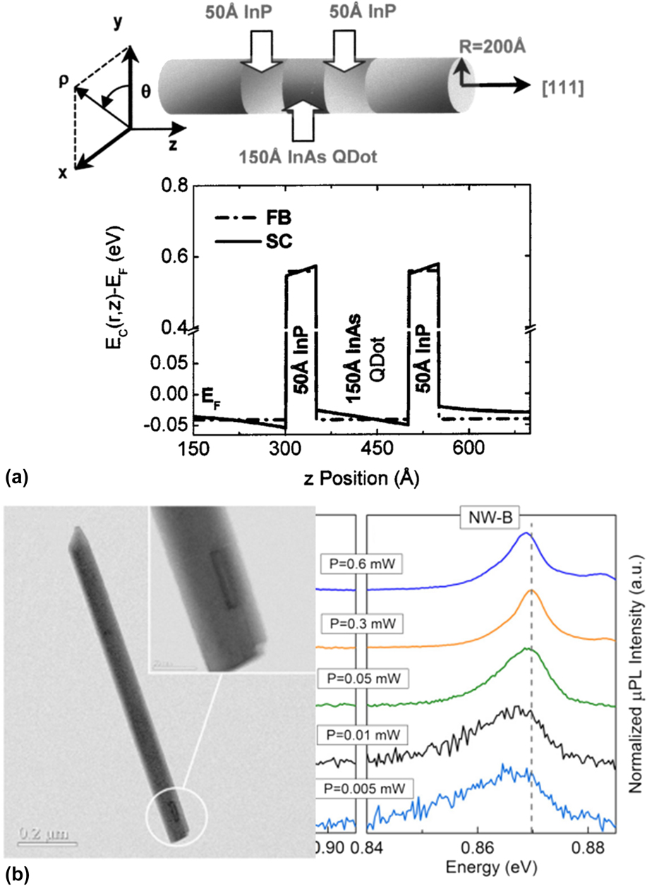
In addition to theoretical studies, several authors have used these strain-induced effects to explain experimental results. Reference Hocevar, Giang, Songmuang, den Hertog, Besombes, Bleuse, Niquet and Pelekanos73–Reference Chen, Lehmann, Nilsson, Kivisaari, Linke, Dick and Thelandert77 Zervos and Feiner have used the lattice-mismatch–induced strain in an axial InAs/InP NW-based resonant tunneling diode, to model experimentally observed shifts in the tunneling resonance in the two opposite current orientations. They have modeled the electric field resulting in the strained regions, giving rise to directionality in the structure Reference Zervos and Feiner74 [see Fig. 5(a)]. Anufriev et al. have examined the photoluminescence of a WZ InAs quantum rod embedded within a WZ InP NW and found results coinciding with the quantum confined Stark effect. Although neglecting spontaneous polarization in the materials, they have considered internal-strain–related piezoelectric fields to model the results Reference Anufriev, Chauvin, Khmissi, Naji, Patriarche, Gendry and Bru-Chevallier75 [see Fig. 5(b)].
Internal piezoelectric effects: (a) schematic structure (top) and calculated conduction band of the InP/InAs double barrier resonant tunneling diode structure, with self-consistent solution containing the piezoelectric fields in the structure. Reprinted with permission from AIP Reference Zervos and Feiner74 ; (b) TEM showing an InAs quantum rod embedded within an InP NW (left) and Stark effect characteristic low excitation blue shift measured in these structures (right). Reprinted with permission from AIP. Reference Anufriev, Chauvin, Khmissi, Naji, Patriarche, Gendry and Bru-Chevallier75

B. Electromechanical effects related to external strain
Next, we turn to examine the influence of externally applied mechanical stress/strain on the electronic/optoelectronic properties of III–V NWs. Reference Chauvin, Mavel, Patriarche, Masenelli, Gendry and Machon78–Reference Signorello, Karg, Bjork, Gotsmann and Riel84 Existing studies have been concerned with the application of axial pressure on the optical properties of WZ Reference Signorello, Lortscher, Khomyakov, Karg, Dheeraj, Gotsmann, Weman and Riel83 and ZB Reference Signorello, Karg, Bjork, Gotsmann and Riel84 GaAs NWs and of hydrostatic pressure on the optical properties of WZ InP NWs. Reference Chauvin, Mavel, Patriarche, Masenelli, Gendry and Machon78 In general, these studies were focused on the effect of pressure on the NW band-gap, i.e., piezoresistivity. They all report considerable changes in the nature of light–matter interactions with applied pressure, brought about by different evolution of energy subbands with pressure. However, direct consideration of piezoelectric effects, in a similar manner done for heterostructure-related internal stresses, has not been addressed.
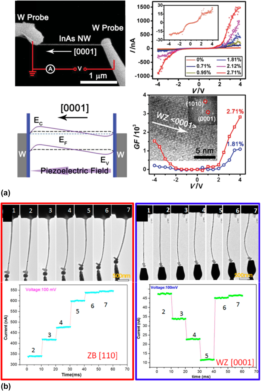
Other studies have dealt with pressure-dependent electronic transport. Li et al. have studied the effect of tensile and compressive axial strain (0–3%) on the conduction of two terminal InAs NW-based devices, with ZB/WZ/mixed phase structures as well as with various axial growth orientation.
Reference Li, Wei, Xu, Pan, Zhao and Chen79
They have calculated the electromechanical gauge factor (relative change in conductance per unit strain) for each NW examined. Interestingly, the only non-negligible result arose when [0001] WZ NWs are measured, while ZB NWs in [011], [103] and
 $\left[ {\bar{2}\bar{1}1} \right]$
orientations and nonpolar
 $\left[ {11\bar{2}0} \right]$
WZ NWs resulted in no observable electromechanical response. The highest electromechanical gauge factor was found for the pure [0001] WZ NWs, while it was found that stacking faults reduce the electromechanical responsivity. The gauge factor was found to have contributions from piezoresistivity (symmetrical with respect to the applied voltage) and the piezotronic effect [asymmetrical even when identical electrodes were used—Fig. 6(a)]. We note that the negligible electromechanical response in nonpolar WZ NWs and ZB NWs remains intriguing considering piezoresistivity is still expected.
Externally applied electromechanical effects: (a) WZ InAs NW piezotronics. Electron microscopy-based stretching scheme (top left), I–V curves for various strain levels (top right), schematic band diagram (bottom left), and electromechanical gauge factor for two strain levels (bottom right). Reprinted with permission from Wiley Reference Li, Wei, Xu, Pan, Zhao and Chen79 ; (b) ZB/WZ InAs NW piezoresistive effect. Left and right show compression experiments on ZB and WZ NWs, correspondingly. The graphs below show the consequent strain related current levels. Reprinted with permission from ACS. Reference Zheng, Zhang, Hu, Chen, Lu, Drennan, Han and Zou80

Indeed, in a further study by Zheng et al., pure phase NWs ([0001] WZ and [110] ZB) were subjected to compressive strains, and the electromechanical transport effects were examined. Reference Zheng, Zhang, Hu, Chen, Lu, Drennan, Han and Zou80 In their experiments, the NWs exhibited ohmic behavior, and so the piezotronic effect was excluded from the explanation, leaving behind piezoresistivity. In a complementary fashion to the previous study, it was found that compressive strain reduced the current in the WZ NW. Interestingly, for the ZB NWs, the current was found to have increased, shedding light on the previously absent piezoresistivity in ZB NWs. Let us consider the differences between this study and the previous one and between the ZB and WZ NW shown [Fig. 6(b)]. First, the gauge factors considered by Li et al. are significantly larger, and therefore the smaller differences considered by Zheng et al. allow better resolution, indicating that indeed piezoresistivity exists for ZB as well as WZ NWs. Second, taking a closer look at the deformations of the WZ and ZB NWs, it seems that the WZ NW undergoes buckling, while the ZB NW undergoes bending. If that is the case, the stress release associated with the buckling may result in the return of the current to its original level. For the ZB NW, the bending may induce compression and tension on different parts of the NW, resulting in current enhancement (on one of the sides). Zheng et al. include a detailed crystal orientation related examination of the piezoresistivity in the NWs. Additional studies were performed on InAs Reference Signorello, Sant, Bologna, Schraff, Drechsler, Schmid, Wirths, Rossell, Schenk and Riel82 and InAsP Reference Lee, Pin, Choi, Jo, Shin, Hong, Lee, Cho, Ahn, Song, Yi and Kim81 NWs. In both cases, the piezoresistivity was examined and used to explain the electromechanical gauge factor. Specifically, for InAs NWs, the pressure dependence of the surface state energy was considered. Reference Signorello, Sant, Bologna, Schraff, Drechsler, Schmid, Wirths, Rossell, Schenk and Riel82 An interesting pattern emerges when considering the previous two sections: when external mechanical stresses are applied, the majority of studies focus on piezoresistivity. This might be due to the fact that most transport studies focus on InAs, usually yielding ohmic contacts thereby rendering the piezotronic effect negligible. Furthermore, most of these studies focused on “simple” (junctionless, nonheterostructure) NWs, where polarization effects are again negligible. This is unlike the studies which considered junctions and explored internal strain-related piezoelectric effects. However, considering piezotronics using III–V NWs for future applications might still be beneficial. In re-examining the results by Li et al., which remain the single study to date dealing with III–V NW piezotronics, the largest gauge factor was associated with the piezotronic effect, while the piezoresistivity-related contribution was smaller (as seen in other studies). We offer an intuitive explanation for this: while fundamentally piezoelectricity and piezoresistivity are linear (disregarding higher order phenomena for now), the current across a semiconductor barrier is exponentially dependent upon its height. Therefore, it might be that piezotronic devices are inherently more sensitive compared to piezoresistive devices, indicating that further research in this direction is worthwhile.
C. Direct examination of piezoelectricity in III–V NWs
In the previous sections, we have examined the application of internal piezoelectric field effects to explain asymmetries in the electrical conductance and photoluminescence of III–V NW heterostructures, and we have surveyed the current literature on external electromechanical effects in III–V NWs, mostly dedicated to piezoresistivity. In this section, we focus on an aspect which is as fundamental as much as it is unavoidable for future consideration of piezoelectric-based III–V applications: the basic piezoelectric properties of III–V NWs. In this case, the body of the work is even smaller than for the previous topics, consisting of four papers that we are aware of. Three of these deal with the piezoelectric properties of GaAs NW ensembles, Reference Soshnikov, Afanas’ev, Petrov, Cirlin, Bouravlev, Samsonenko, Khrebtov, Tanklevskaya and Seleznev85–Reference Lysak, Soshnikov, Lahderanta and Cirlin87 and the other one, and the first study to date to directly examine the piezoelectricity in single III–V (InP and GaAs) NWs, is our own recent publication. Reference Calahorra, Guan, Halder, Smith, Cohen, Ritter, Penuelas and Kar-Narayan1
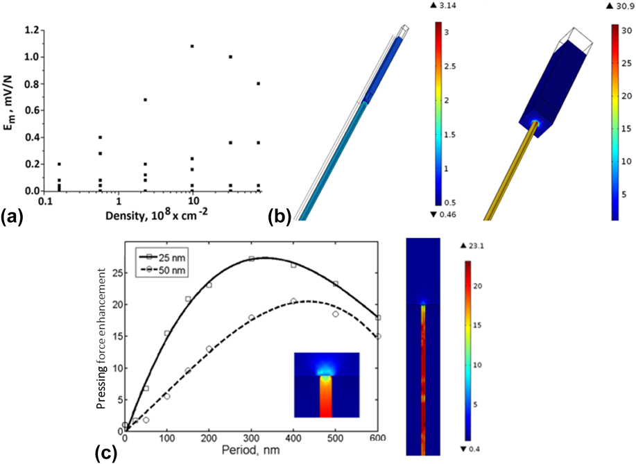
In the first study by Soshnikov et al., a mixed phase (mostly WZ) GaAs NW ensemble was embedded in poly(methyl methacrylate) (PMMA) and contacted from top and bottom to fabricate a vertically aligned NW-based capacitor structure, Reference Soshnikov, Afanas’ev, Petrov, Cirlin, Bouravlev, Samsonenko, Khrebtov, Tanklevskaya and Seleznev85 similar to typical piezoelectric nanogenerator structures. The sample was subjected to acoustic excitation, and the generated voltage recorded. An effective d 33 value of about 22 pm/V was extracted following setup calibration. These experimental results were further analyzed, drawing attention to the order of magnitude increase in the extracted coefficient compared to the theoretically expected value for WZ GaAs d 33 of about 2.3 pm/V. Reference Lysak, Soshnikov, Lahderanta and Cirlin86,Reference Lysak, Soshnikov, Lahderanta and Cirlin87 Following finite element simulations, the dominant effect in the observed increase of the effective piezoelectric coefficient was attributed to “pressure force enhancement”, a geometrical factor brought by the ratio between the top electrode surface area and the NW diameter. A similar factor related to the “fill-factor” of the NWs on the substrate is examined, where the effect of the PMMA material in between the NWs is demonstrated. The simulations successfully recreate the experimental trend of an optimum NW density for increasing the electromechanical coupling (Fig. 7), and in manifesting the importance of geometry in determining the effective piezoelectric behavior of a given configuration.
The piezoelectric properties of GaAs NW ensembles: (a) experimentally measured electromechanical coupling as a function of NW density; (b) finite element simulation of the pressure force enhancement effect; (c) simulation of the intra-NW medium, recreating the NW density effect. Reprinted with permission from Wiley. Reference Lysak, Soshnikov, Lahderanta and Cirlin86

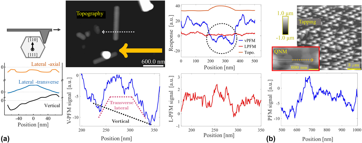
Recently we have examined single III–V NWs using a nondestructive PFM apparatus Reference Calahorra, Guan, Halder, Smith, Cohen, Ritter, Penuelas and Kar-Narayan1 developed in our group. Reference Calahorra, Smith, Datta, Benisty and Kar-Narayan88 Briefly, PFM is a scanning probe technique, where an AFM tip in contact mode applies an electrical field to a piezoelectric sample, thus inducing converse-piezoelectric deformations, which are picked up by the same tip. Reference Gruverman and Kalinin89 By superimposing an electrical signal on a mechanically oscillated tip probing the sample, we have realized a nondestructive PFM method. Reference Calahorra, Guan, Halder, Smith, Cohen, Ritter, Penuelas and Kar-Narayan1 Specifically, mixed phase (predominantly ZB) GaAs NWs were measured in a horizontal configuration, while WZ InP NW stems were examined in a vertical configuration. Figure 8(a) shows a GaAs NW scanned across its length, and the related COMSOL-computed deflection levels in three directions (out-of-plane, axial in-plane, and transverse in-plane). It was found that the experimental vertical PFM signal obtained from the NW could be explained as a superposition of the simulated vertical deflection and the transverse in-plane deflection, coupled to the vertical sensor through cantilever buckling. Furthermore, the simulated axial in-plane deflection bore a resemblance to the measured lateral signal (in the axial direction). Figure 8(b) shows the results obtained for vertically oriented InP NWs, showing a clear distinction from the surroundings (SiN x dielectric). Following calibration, a value of 1 pm/V was extracted from this measurement, which is reasonable considering the known properties of InP. Interestingly, this value is 5 times larger than the minimal theoretical values obtained for InP, and 5 times smaller than the maximal value (see Table I). Nonetheless, further characterization is required to validate this result and to decouple intrinsic material properties from geometrical effects in the NWs.
The piezoelectric properties of single III–V NWs probed by PFM: (a) horizontally measured ZB GaAs NW (scheme—top left and AFM capture—top middle), where the results from finite element simulations (left) successfully recreated the experimentally obtained lateral and vertical PFM signals (bottom middle and right); (b) vertically aligned WZ InP NWs (AFM capture—top, PFM scanned NWs—inset) and the resulting PFM from the substrate and the NW (bottom), used to extract a d 33 value. Reprinted with permission from IOP. Reference Calahorra, Guan, Halder, Smith, Cohen, Ritter, Penuelas and Kar-Narayan1

Both studies demonstrate how the system geometry has a significant influence on piezoelectric performance, either by device characteristics or measurement apparatus specifics (e.g., nonuniform field in a tip/NW/substrate configuration). These effects render the interpretation of experimental results challenging, conveying the importance of simulations as well as highlighting the necessity of further study in this topic for better understanding of fundamental and device-related piezoelectric performance.
Furthermore, both these studies indicate the piezoelectric coefficients at the 10–100 nm scale are similar to those theoretically predicted. This stands in some contrast to the results obtained for GaN NWs, where the axial piezoelectric strain coefficient (d 33) was found to be 3–6 times higher than that reported for bulk. Reference Minary-Jolandan, Bernal, Kujanishvili, Parpoil and Espinosa8,Reference Tiwary, Sarkar, Rao and Laha90 Minary–Jolandan et al. further reported a similar increase in the two other piezoelectric coefficients. Reference Minary-Jolandan, Bernal, Kujanishvili, Parpoil and Espinosa8 Although we are unaware of a study directly comparing NWs and bulk material, Tiwary et al. went on to perform such finite element simulations. Reference Tiwary, Sarkar, Rao and Laha90 Their results indicate that the inherent softening of the NW compared to thin films (reduced mechanical constraints) might be behind the increased electromechanical response. In addition, first-principle studies predict the increase of effective piezoelectric coefficients at the extreme (1–10 nm) nanoscale Reference Agrawal and Espinosa91,Reference Hoang, Yvonnet, Mitrushchenkov and Chambaud92 ; however, the application of these results to NWs an order of magnitude thicker would not be easily justified. In any case, the current picture arising form available data is that although further study of this topic is required, NW-based geometry might promote electromechanical applications due to enhanced responsivity.
IV. SUMMARY AND OUTLOOK
To conclude, we have surveyed the research done in recent years with regard to electromechanical and piezoelectric effects in non-nitride III–V NWs which, due to their distinct crystalline nature as compared to the bulk, present tremendous scope for both fundamental investigations as well as applications. Several trends arise which could further direct the study in this topic: first, regarding the mechanical properties of WZ III–Vs, it seems that the theoretical predictions hold for the elastic modulus in NWs with diameters greater than 10 nm; second, the unique geometry and crystalline properties of III–V NWs (relaxed mechanical constraints, growth in <111> orientation or WZ phase) imply that enhanced electromechanical properties may arise and thus should encourage further work in this area. Nevertheless, several aspects are crucial for further understanding of III–V NW piezoelectricity: (i) the role of stacking faults on the mechanical properties, and on piezoelectricity (as charge traps etc.); (ii) the role of nonlinear piezoelectricity in III–V NWs Reference Al-Zahrani, Pal, Migliorato, Tse and Yu54 ; and (iii) the complexities related to piezoelectric III–V semiconductors, particularly due to being more conductive compared to III-Ns and giving rise to issues such as surface states and surface oxides. In all cases, development of robust and reliable nanocharacterization tools capable of measuring spatially resolved electromechanical properties of nanoscale materials is crucial to drive the field forward.
Considering the above and the vast interest in electronic and optoelectronic applications of III–V NWs, further examination of the piezoelectric effect is an interesting research topic from both a fundamental and practical point of view and could have potential useful applications opening up additional avenues for device improvement, particularly in the emerging areas of piezotronics and photopiezotronics. The study of piezoelectricity in non-nitride III–V materials is particularly attractive considering the vast knowledge base related to these materials in terms of processing and, in particular, in the possible combinations with optical properties in wavelengths spanning the near infra-red spectrum.
ACKNOWLEDGMENT
S.K-N and Y.C are grateful for financial support from the European Research Council through an ERC Starting Grant, NANOGEN (Grant No. ERC-2014-STG-639526).