I. INTRODUCTION
With the continuous development in modern communication systems, high data rate, high transmission capacity, and multi-service in wireless communication systems, such as multichannel multipoint distribution services, wireless local area network, automatic vehicle identification systems, are highly demanded. As one of the most pivotal passive components in radio frequency front-end, multi-band bandpass filters (BPFs) have been wildly investigated during the last decades. Various methods have been proposed to develop multi-band BPFs [Reference Li, Huang and Zhao1–Reference Wu, Jian, Chen and Su17], among which using multi-mode resonator to design multi-band BPFs is an attractive approach [Reference Li, Huang and Zhao1–Reference Hsu, Chien and Tu6]. For this method, multiple resonant modes can be divided into several groups to form a multi-band BPF with appropriate arrangement of the resonant modes. As a straightforward method, multi-band BPFs can be extended by combining several individual resonators or BPFs together using common input and output port [Reference Denis, Song and Zhang7–Reference Xu, Zhang, Zhuge and Fan11]. For this method, the center frequencies (CFs) and the bandwidth of the passbands are controllable independently, but it is limited by the number of the cascaded resonators and BPFs, and it suffers from relatively larger circuit area. The third method to achieve multi-band BPFs is to cascade BPF with bandstop filter [Reference Liu, Huang and Wu12, Reference Tsai and Hsue13]. These filters have excellent performance in band-to-band isolation, however, it is usually implemented by using via holes and occupies large circuit area. Besides, using signal multi-path propagation to realize multi-band BPF is also believed to be practical [Reference Weng, Liu, Wu and Hung14–Reference Wu, Jian, Chen and Su17].
Although the filters [Reference Li, Huang and Zhao1–Reference Wu, Jian, Chen and Su17] have fully demonstrated their own merits, it may be embarrassed for their narrow bandwidths [Reference Liu3–Reference Gao, Zhang and Xue5, Reference Denis, Song and Zhang7, Reference Liu10, Reference Xu, Zhang, Zhuge and Fan11, Reference Wu, Chen and Chen16, Reference Wu, Jian, Chen and Su17], which is difficult to meet the requirement of high data rate, high transmission capacity, and multi-service in modern communication systems. Recently, a dual-wideband BPF based on a single penta-mode resonator with controllable CFs is reported in [Reference Li, Huang and Zhao1]. However, the upper stopband performance should be improved much further. In [Reference Wu, Liao and Xiong2, Reference Hsu, Chien and Tu6], the authors use T-shaped resonator to design dual-wideband BPF. Good out-of-band performance is achieved in [Reference Wu, Liao and Xiong2], but the passbands performances with only one transmission pole in each passband and non-independent controllable CFs should be further enhanced. So far, only few attempts have been proposed to design a dual-wideband BPF with independently controllable CFs and wide stopband suppression using a single multiple mode resonator (MMR).
In this paper, a dual-wideband BPF with independently controllable CFs and good out-of-band rejection is presented based on the method of using a single MMR. The CFs of the dual-wideband BPF centered at 2.96 and 5.695 GHz with 3-dB fractional bandwidths (FBWs) of 27.7 and 23.4%, respectively. In addition, multiple transmission zeros (TZs) are generated, which can be employed to achieve wide stopband suppression. The resonant characteristics of the quintuple-mode resonator (QMR) are analyzed with the help of the odd- and even-mode analysis technique. For validation, a dual-wideband BPF is designed, fabricated, and measured. It shows that the measurement results are in good agreement with the prediction ones.
II. CHARACTERISTICS OF THE QMR
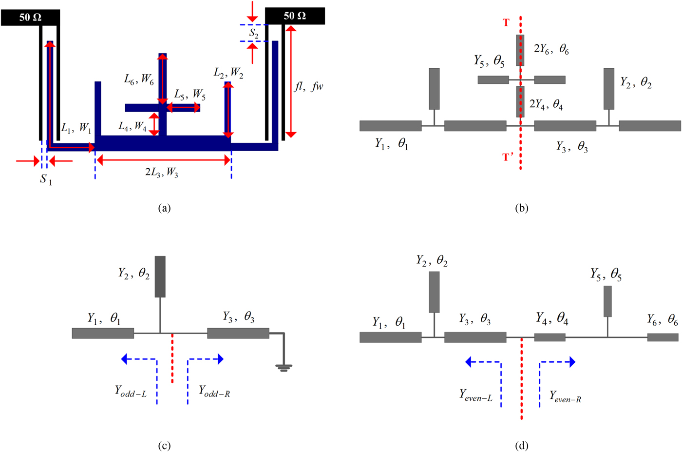
As shown in Figs 1(a) and 1(b), the proposed QMR consists of an inverted Pi-shaped resonator (IPSR) (denoted by (L 1, W 1), (L 2, W 2) and (L 3, W 3)) and an open cross-shaped resonator (CSR) (denoted by (L 4, W 4), (L 5, W 5), and (L 6, W 6)). Since the structure is symmetrical with T-T’ plane, the even-mode and odd-mode analysis technique has been employed to analyze the structure. The odd-mode and even-mode equivalent circuits are shown as Figs 1(c) and 1(d), respectively.
Proposed QMR (a) layout, (b) TLM, (c) odd-mode equivalent circuit, (d) even-mode equivalent circuit.

As sketched in Fig. 1(c), Y odd-L and Y odd-R denote the input admittances from the left side and right side of the reference plane in the case of odd mode excitation, respectively. According to the transverse resonant condition, it can be derived as
 $${\rm Im}\left( {Y_{odd - L} + Y_{odd - R}} \right) = 0,$$
where,
 $$Y_{odd - L} = j\left( {Y_{\rm 1}{\rm tan}\theta _{\rm 1} + Y_{\rm 2}{\rm tan}\theta _{\rm 2}} \right),$$
 $$Y_{odd - R} = {\rm} - jY_{\rm 3}{\rm cot}\theta _{\rm 3}.$$
Similarly, in the case of even mode excitation, it should satisfy
 $${\rm Im}\left( {Y_{even - L} + Y_{even - R}} \right) = 0,$$
where,
 $$Y_{even - L} = \displaystyle{{jY_3(Y_1 {\rm tan} \theta _1 + Y_2 {\rm tan} \theta _2 + Y_3 {\rm tan} \theta _3)} \over {Y_3 - (Y_1 {\rm tan} \theta _1 + Y_2 {\rm tan} \theta _2) {\rm tan} \theta _3}},$$
 $$Y_{even - R} = \displaystyle{{jY_4(Y_6 {\rm tan} \theta _6 + Y_5 {\rm tan} \theta _5 + Y_4 {\rm tan} \theta _4)} \over {Y_4 - (Y_6 {\rm tan}\theta _6 + Y_5 {\rm tan} \theta _5) {\rm tan} \theta _4}}.$$
Here, Y n (n = 1, 2,…, 6) and θ n (n = 1, 2,…, 6) denote the characteristic admittances and electrical lengths of the stubs, respectively. For simplicity, we let the CF f 0 = 3.0 GHz, Y 1 = Y 2 = … = Y 6 = 1/100. Substituting (2) and (3) into (1), then, we have
 $${\rm tan}\theta _{\rm 1} + {\rm tan}\theta _{\rm 2} - {\rm cot}\theta _{\rm 3} = {\rm} 0.$$
Similarly, substituting (5) and (6) into (4), then, we have
 $$\eqalign{& \left( {{\rm tan}\theta _{\rm 6} + {\rm tan}\theta _{\rm 5} + {\rm tan}\theta _{\rm 4}} \right)\left( {{\rm 1} - {\rm tan}\theta _{\rm 3}\left( {{\rm tan}\theta _{\rm 1} + {\rm tan}\theta _{\rm 2}} \right)} \right) \cr & + \left( {{\rm tan}\theta _{\rm 1} + {\rm tan}\theta _{\rm 2} + {\rm tan}\theta _{\rm 3}} \right)\left( {{\rm 1} - {\rm tan}\theta _{\rm 4}\left( {{\rm tan}\theta _{\rm 5} + {\rm tan}\theta _{\rm 6}} \right)} \right) = 0.} $$
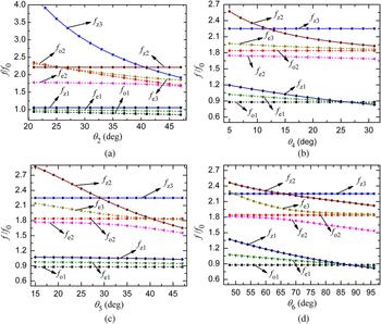
As an example, we set θ 1 = 60°, θ 2 = 40°, and θ 3 = 30° in the case of odd mode excitation. It is worth noting that the initial values of the electrical lengths are calculated at f 0. So, when the incident frequency f i is considered, all of the electrical lengths should be recalculated as  $\theta _n{\!\!^\prime} = \theta _nf_i/f_0$ (n = 1, 2, 3). Then, we substitute all of the new values of the electrical lengths into (7). If the equation (7) is satisfied, it means that f o1 = f i is the one odd-mode resonant frequency that we are looking for. If f i sweeps from 0 to 10 GHz, then we can obtain all of the odd-mode resonant frequency in this range. This is also true in the case of even-mode excitation. As shown in Fig. 2, the resonant frequencies of the QMR with varied θ 2, θ 4, θ 5, and θ 6 are given under the condition of θ 1 + θ 3 = 90°. It can be found that five resonant modes f o1, f o2, f e1, f e2, and f e3 have been excited, among which f o1 and f o2 denote the odd-mode resonant frequencies, while f e1, f e2, and f e3 denote the even-mode resonant frequencies. In addition, three inherent TZs, f z1, f z2, and f z3, are clearly observed, among which f z1 divides the five resonant modes into two groups, i.e., the first two resonant modes and the other three modes. It can be observed from Fig. 2(a) that f e2, f e3, and f o2 decrease with the increase of θ 2, while f o1 and f e1 change slightly. In addition, f z3 decreases dramatically as θ 2 gets larger, whereas f z1 and f z2 keep constant. It can also be observed from Figs 2(b)–2(d) that f e1, f e2, f e3, f z1, and f z2 decrease with the increase of θ 4, θ 5, and θ 6, whereas f o1, f o2, and f z3 keep constant.
Resonance properties versus (a) θ 2, (b) θ 4, (c) θ 5, and (d) θ 6.

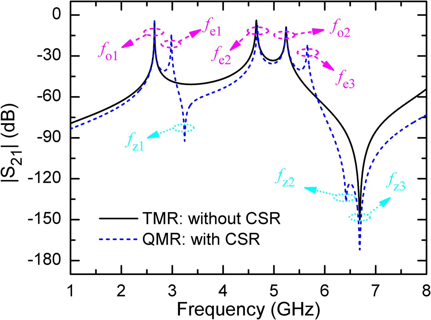
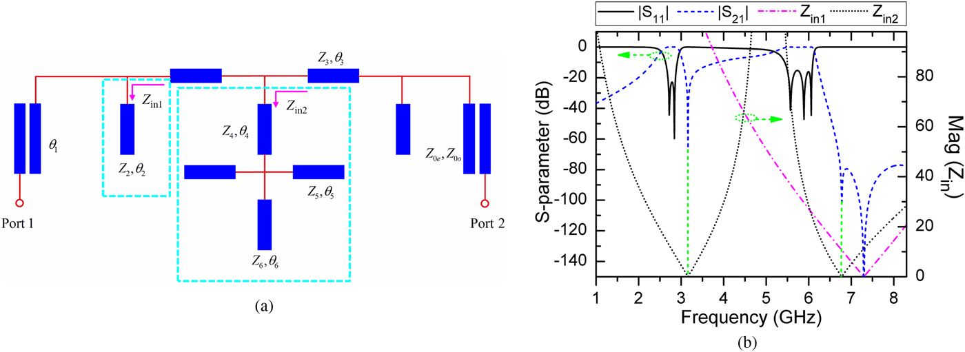
Fig. 3 depicts the frequency responses of IPSR and QMR under a weak coupling. With CSR loaded in the center of IPSR, extra two resonant modes f e1 and f e3 can be generated. Besides, the extra introduced TZ f z1 divides the five resonant modes into two groups. As shown in Fig. 4, we investigated the frequency responses of S-parameters and Z in, where Z in1 and Z in2 denote the input impedance of the corresponding stubs enclosed by the cyan rectangular box. As long as Z in = 0 is satisfied at a certain frequency, a TZ will be generated at this frequency. This is attributed to the introduction of virtual ground, which short out the transmission signals. Therefore, the signals transmitted from port 1 to port 2 are blocked. Thus, we can derive the following equations:
 $$Z_{{\rm in}1} = - jZ_2\cot (\theta _2) = 0,$$
 $$ Z_{{\rm in2}} = - \displaystyle{{Y_4 - 2Y_5 {\rm tan} \theta _4 {\rm tan} \theta _5 - Y_6 {\rm tan} \theta _6 {\rm tan} \theta _4} \over {jY_4(Y_4 {\rm tan} \theta _4 + 2Y_5 {\rm tan} \theta _5 + Y_6 {\rm tan} \theta _6)}} = 0.$$
Frequency responses of IPSR and QMR.

(a) Ideal model circuit of quintuple-mode resonator, and (b) frequency responses of |S 21| and Z in.

According to the equations, (9) and (10), TZs can be determined and moved by tuning the corresponding stubs.
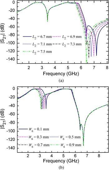
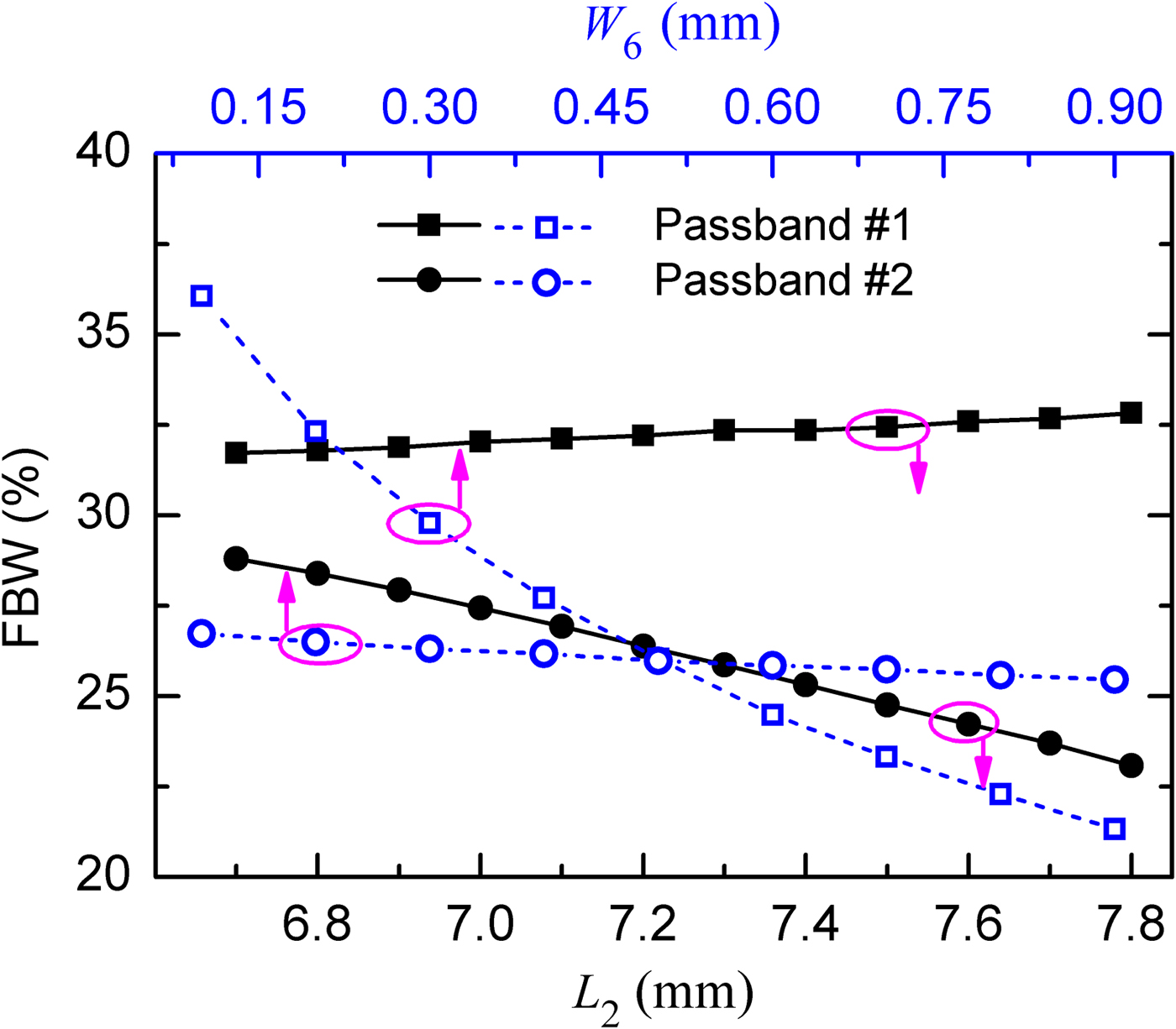
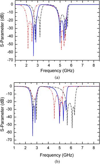
Frequency responses of |S 21| versus varied L 2 and W 6, which is simulated using transmission line model (TLM) in Fig. 1(b) are plotted in Figs 5(a) and 5(b). It can be found that L 2 mainly impacts on the higher passband, but it almost has no influence on the lower passband. However, the results are quite different for changing W 6, where W 6 mainly affects the first passband, whereas it has slightly influence on the second passband. As shown in Fig. 6, 3-dB FBWs with varied L 2 and W 6 are recorded according to the Figs 5(a) and 5(b). It can be observed that FBWs of the first passband and the second passband can be independently controlled by changing W 6 and L 2, respectively. For demonstration, an example, which two CFs can be independently selected is given (unit: mm): L 1 = 12.9, L 2 = 7.2, L 3 = 3.7, L 4 = 0.9, L 5 = 5.9, L 6 = 13, fl = 12.6, S 1 = 0.15, S 2 = 0.8, fw = 0.2, W 1 = W 2 = … = W 6 = 0.2. Its simulated results are plotted by blue solid line in Figs 7(a) and 7(b). By changing the TLM circuit parameters, two passbands of the dual-wideband BPF can be controlled independently. In Fig. 7(b), for example, the results plotted by red dash dot line are obtained by changing the circuit parameters as (unit: mm): L 1 = 13.8, L 2 = 6.9, L 3 = 3.6, L 4 = 1.3, L 5 = 5.9, L 6 = 13.2, fl = 13.8, S 1 = 0.05, S 2 = 2.7, fw = 0.2, W 1 = 0.45, W 2 = 0.2, W 3 = 0.15, W 4 = W 5 = 0.1, W 6 = 0.2. It can be observed from Figs 7(a) and 7(b) that each of the passbands can be independently selected.
|S 21| versus varied (a) L 2 and (b) W 6.

FBWs versus varied L 2 and W 6.

(a) Controllable 1st passband and the fixed 2nd passband, and (b) controllable 2nd passband and the fixed 1st passband.

III. IMPLEMENTATION OF DUAL-WIDEBAND BPF
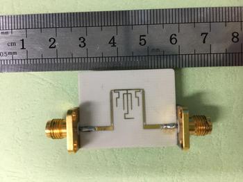
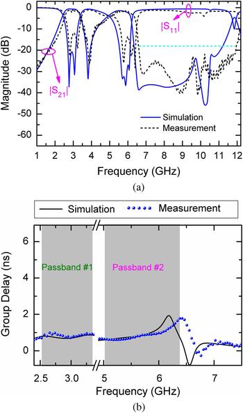
As an example, a dual-wideband BPF, which f c1 and f c2 are designed at 2.9 and 5.5 GHz, respectively, is presented. As shown in Fig. 2, the lower passband is formed by the first two modes, i.e., f o1 and f e1, while the other three modes, namely f o2, f e2, and f e3, contribute to the higher passband. For verification, a dual-wideband BPF is fabricated on the substrate of Rogers4003C with parameters of ε r = 3.55, h = 0.508 mm, and tan δ = 0.0027, which is shown in Fig. 8. The dimensional parameters of the dual-wideband BPF are given as follows (all in millimeter): L 1 = 11.2, L 2 = 7.3, L 3 = 4.3, L 4 = 1, L 5 = 6.2, L 6 = 11.4, W 1 = W 2 = W 4 = W 5 = W 6 = 0.2, W 3 = 0.3, S 1 = 0.15, S 2 = 0.8, fl = 10.7, fw = 0.1. The overall size of the filter occupies 10.5 mm × 10.6 mm (excluding feeding lines), which corresponds to the size of 0.17λ g × 0.17λ g, where λ g is the guided wavelength at 2.96 GHz. Figure 9 plots the simulation and measurement results of S-parameters and group delay. It can be seen that wide stopband suppression from 6.6 to 11.93 GHz with 20 dB attenuation is achieved. The measured CFs of the two passbands centered at 2.96 and 5.695 GHz, and the minimum insertion losses are 0.86 and 1.1 dB. It can also be observed from Fig. 9(a) that the 3-dB FBWs of the two passbands are 27.7 and 23.4%, respectively. Table 1 lists a comparison between some published dual-wideband BPFs and this work in terms of CFs, 3-dB FBWs, 20-dB suppression, circuit size, and independently controllable CFs. It can be seen that the presented BPF exhibits good performances such as compact size, wide bandwidth, wide stopband suppression, and independently controllable CFs.
Photograph of the proposed dual-wideband BPF.

(a) Simulated and measured frequency responses of the dual-wideband BPF, (b) group delay.

Comparison with some proposed dual-wideband BPFs.

IV. CONCLUSION
In this paper, a compact dual-wideband BPF with wide upper-stopband suppression using a new QMR, which is analyzed by odd-/even-mode analysis method, is presented. It shows that the QMR can excite five resonant modes, in which the first two modes are used to design the lower passband and the other three modes are employed to form the higher passband. Good performances such as compact size, wide bandwidth, wide stopband suppression, and independently controllable CFs are achieved. The measurement results are in good agreement with the prediction results, which verify the validity of the dual-wideband BPF.
ACKNOWLEDGEMENTS
This work was supported in part by the National Natural Science Foundation of China under Grants (61171028, 61176119, and 61471208), and in part by the Tianjin Research Program of Application Foundation and Advanced Technology (15JCQNJC01300, and 15JCYBJC46900).
 Yang Xiong was born in Huaihua, Hunan province, China, in 1990. He received his B.E. degree in communication engineering from Shandong University of Technology, Zibo, China, in 2013, and is currently working toward his Ph.D. degree in electronic science and technology at Nankai University, Tianjin, China. His main research interests include microwave circuit design, high-temperature superconducting microwave devices, and terahertz signals detection.
 LiTian Wang was born in Tianjin, China. He received the B.E. degree from Tianjin University of science of technology Tianjin China in 2014 and is currently working toward the Ph.D. degree at Nankai University, Tianjin, China. His main research interests include microwave passive components and systems, HTS tunable filters design.
 DouDou Pang received the B.E. degree from Nankai University, Tianjin, China, in 2015, and is currently working towards the M.E. degree. Her main research interests are microwave filters and antenna design.
 Wei Zhang received the B.E. degree from Nankai University, Tianjin, China, in 2015, and is currently working toward the M.E. degree. His main research interests are microwave filters and multiplexers design.
 Fan Zhang received the B.E. degree from Nankai University, Tianjin, China, in 2015, and is currently working toward the M.E. degree. His main research interests are microwave filters and multiplexers design.
 Ming He received the M.E. and Ph.D. degrees in electrical engineering from Nankai University, Tianjin, China, in 2002 and 2008, respectively. Since 1997, he has been with the Department of Electronics, Nankai University, Tianjin, China, where he became a Professor in 2016. From 2004 to 2009, he held several visiting research appointments in Juelich Research Center and Karlsruhe University, Germany. His research interests are in the fields of the applications of high temperature superconductors, the generation and detection of THz signals, and microwave communications.
 XinJie Zhao received his M.E. degree in semiconductor physics from University of the Inner Mongol, Huhehaote, China, in 1988, and Ph.D. degree in material science from China Institute of Atomic Energy, Beijing, China, in 1999, respectively. Since 2002, he has been Professor with the Department of Electronics, Nankai University, Tianjin, China. His research interests are in the fields of the applications of high temperature superconductors, the generation and detection of THz signals, and Microwave device.
 Xu Zhang received the Ph.D. degree in electrical engineering from Nankai University, China, in 2008. He is currently an associate professor at College of Electronic Information and Optical Engineering, Nankai University. His research interests include the applications of high temperature superconductors, superconducting filter and microwave communications.