I. INTRODUCTION
Modern wireless communication systems use digital modulation signals that must be transmitted linearly while preserving a high-power efficiency. Among all existing architectures, the LInear amplification using Non-linear Components (LINC) architecture is a promising solution for base station transmitters [Reference Cox1–Reference Raab3]. The key issue of this architecture is that the power amplifiers (PA) must be a perfect voltage source and the choice of the class of the PA is primordial to achieve this operation mode [Reference Yao and Long4]. In this paper, we study the impact of some PA classes, namely, AB, B, C, D, E, F, and J, on both efficiency and linearity of the LINC transmitter. The comparative analysis of PAs is performed through extensive simulations using Agilent's advanced design system. The advantages and drawbacks of this architecture are then demonstrated. PAs are simulated using a gallium-nitride high electron mobility transistor (GaN HEMT) model from Cree to achieve an output power of 10 W at 900 MHz. Linearity and efficiency performances of the transmitter are evaluated in terms of error vector magnitude (EVM), adjacent channel leakage ratio (ACLR), power added efficiency (PAE), using a 16QAM modulation.
This paper is organized as follows: Section II describes the operation principle of the LINC architecture. The combiners for signal recombination at the output are presented in Section III. The performances of the simulated radio-frequency (RF) PAs are presented in Section IV. In Section V, we elaborate on how the performance of LINC transmitters is heavily dependent on the class of the PAs used. A 16QAM modulated signal is used for this study. Finally, conclusions are given in Section VI.
II. LINC ARCHITECTURE
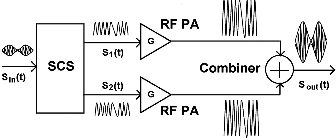
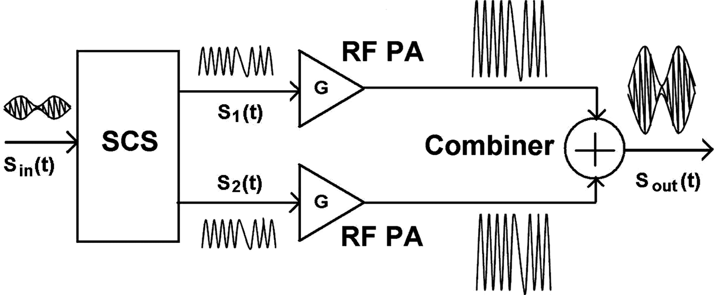
The principle of operation of the LINC transmitter is depicted in Fig. 1. The input signal S in(t), with variable envelope r(t) and phase φ(t), is separated into two constant envelope signals, S 1(t) and S 2(t), by the signal component separator (SCS):
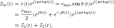
where


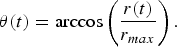
with r max the maximum value of r(t) and θ(t) equal to
LINC system topology.
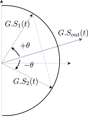
The principle of signal decomposition is illustrated in Fig. 2 using a vectorial representation.
LINC vectorial representation.

Signals S 1(t) and S 2(t) are amplified with two power efficient PAs with a power gain G. Envelope amplitude variation is restored at the output of the combiner by the simple addition of the two amplified signals. The output signal is then given by

III. SIGNAL RECOMBINATION
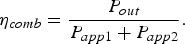
The restoration of the original signal waveform at the output of the LINC transmitter is realized by an RF combiner. In the literature, we can find two types of combiners: Wilkinson combiner which is matched and lossy and Chireix combiner which is unmatched and lossless [Reference Birafane, El-Asmar, Kouki, Helaoui and Ghannouchi5]. Combiner efficiency, denoted η comb, is defined in equation (6) as the ratio of the active power P out delivered to the output load to the sum of the apparent power in the input of each line P app1 and P app2 [Reference Raab2, Reference Chireix6]:
A) Wilkinson combiner
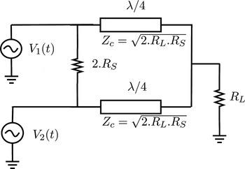
The topology of this combiner is given in Fig. 3. Z c is the characteristic impedance of the two quarter-wavelength transmission lines, R S represents the impedance seen at each input of the combiner, and R L is the output load of the combiner.
Wilkinson combiner.

The two outphased input signals denoted V 1(t) and V 2(t) and having a constant amplitude V, can be written as
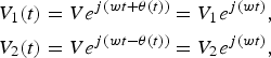
where V 1 and V 2 are complex conjugates
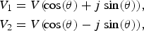
thus we can demonstrate that the Wilkinson efficiency, ηWilkinson, can be expressed as a function of the outphasing angle θ (t) as follows [Reference Birafane, El-Asmar, Kouki, Helaoui and Ghannouchi5]:

The efficiency of this combiner is linked to the fact that the two PAs deliver a constant maximum power at both inputs of the combiner and the output power depends only on the envelope of the signal, that is to say r(t) and thus the outphasing angle θ(t) as defined in equation (4).
B) Chireix combiner
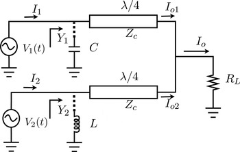
The Chireix combiner is composed of two quarter-wavelength transmission lines having a characteristic impedance Z c and connected to the output load of combiner R L [Reference Chireix6], as presented in Fig. 4.
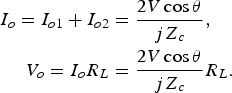
Let us first make the analysis of this combiner (Fig. 4), without the inductor L and the capacitor C (non-compensated Chireix combiner). The output current I o and output voltage V o are given in equation (10) from general equations of transmission lines, where I o1 and I o2 are the two output currents:
Chireix combiner with compensation.

The input currents are

Thus, the admittances Y 1 and Y 2, seen by each PA, are complex conjugate:
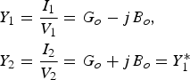
with G o and B o
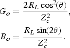
In order to increase the combiner efficiency, susceptance B o should be compensated for, at a chosen angle θcomp, by introducing a parallel admittance calculated from equation (13) using either stubs or passive elements, e.g. C and L with dotted lines in Fig. 4 and with the values
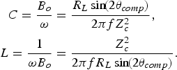
Equations (10)–(13) are calculated taking into account only the two sources, both transmission lines and the output load R L in the Fig. 4. From equation (14) and for the following equations, values of L and C will be considered, i.e. the compensation represented by θcomp, unless stated otherwise.
According to the PA class and the compromise between power efficiency and linearity of the overall transmitter, this compensation angle has to be chosen carefully [Reference Birafane, El-Asmar, Kouki, Helaoui and Ghannouchi5, Reference Bi7].
The efficiency of the Chireix combiner is defined as

and is expressed in function of θ, without and with compensation, as follows:


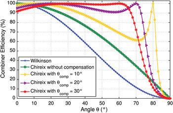
Figure 5 shows both combiners efficiency calculated from equations (9), (16), and (17). For the Chireix combiner, efficiency is evaluated without and with compensation for different values of θcomp: 10o, 20o, and 30o.
Efficiency of Wilkinson combiner and Chireix combiner (with and without compensation)

These results demontrate that the Chireix combiner has a higher efficiency than the Wilkinson combiner. Nevertheless, the Chireix non-isolating behavior modifies its input impedances according to the angle θ from equation (4) and thus the power transmitted by each PA. This highlights the need for performance analysis of the LINC architecture using a Chireix combiner with different PA classes. A LINC transmitter with saturated class B PAs using a Chireix combiner can be founded in [Reference Hakala8]. An analysis using class AB and class F PAs for this architecture is shown in [Reference Montesinos, Berland, Abi-Hussein, Venard and Descamps9].
In addition, the impedances Z 1 and Z 2 seen by each PA are determined from equation (12) as follows:
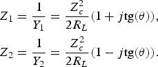
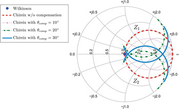
Figure 6 represents these impedances for each combiner, Wilkinson and Chireix (without and with compensation), as a function of the angle θ in the Smith chart. Since Wilkinson combiner is isolated, Wilkinson combiner impedances are placed at the center of the Smith chart, whereas, the input impedances at the input of Chireix combiner are angle dependent, as shown in Fig. 6. As a result, the compensation in Chireix combiner has an important impact on the linearity of the whole system as it modifies the PAs transmitted power. In order to achieve the best transfer of power and avoid the power loss between the PA and the combiner, output load of PAs need to be carefully matched with the impedances Z 1 and Z 2, at an appropriate value of θcomp. Thus, these curves are very useful to analyze the behavior of load modulation of the PAs. Figure 6 is determined with the assumption that the output impedance of PA is 50Ω.
Smith chart for different impedances with Wilkinson and Chireix combiner (with and without compensation). Z 1 and Z 2 represent, respectively, the impedances at the upper and lower branches (θ (0–90o)).

In the following section, we review the classes of RF PAs simulated for this study.
IV. RF POWER AMPLIFIERS
PAs are often classified according to their biasing and their operating classes [Reference Colantonio, Giannini and Limiti10]. A first classification relies on biasing classes PAs (classes A, AB, B, or C): the driving signal is a sinusoidal waveform and the active device behaves as a current source. Classes AB, B, and C PAs are chosen for our study. A second classification is related to the active device dynamic operating conditions and consequently to the matching network terminating conditions. In this case, basically two wide categories are identified, namely current-mode and switching-mode PAs. In the former case, referred, as classes F, F−1, and J, the active device acts as voltage controlled or current controlled current source. Whereas, in the latter family, referred as classes D, E, G, and H, the active devices behave as switches. Class D PAs can operate either in current mode class D (CMCD) or in voltage mode class D (VMCD). For our study, in addition to the biasing classes AB, B, and C, we will consider PA classes from the second category namely CMCD, VMCD, E, F, F−1, and J.
A) Design of classes RF PAs
The various PAs are designed using a 15 W GaN Cree transistor (CGH27015) to achieve an output power of 40 dBm (10W) at 900 MHz. Transistor model includes intrinsic and packaging parasitic components. This transistor model has a typical drain–source breakdown voltage of 140 V. All PAs are designed with 22 V supply voltage source. For this value of drain–source voltage (V ds), the maximal drain current (I ds) is equal to 2.9 A and the typical gate threshold voltage is equal to −3.3 V. The conduction angles for biasing classes PAs are determined in fonction of gate voltages.
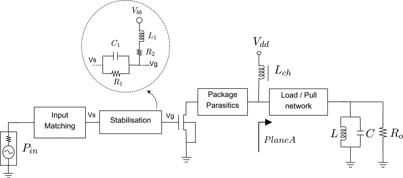
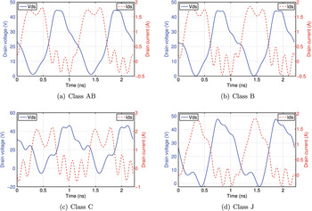
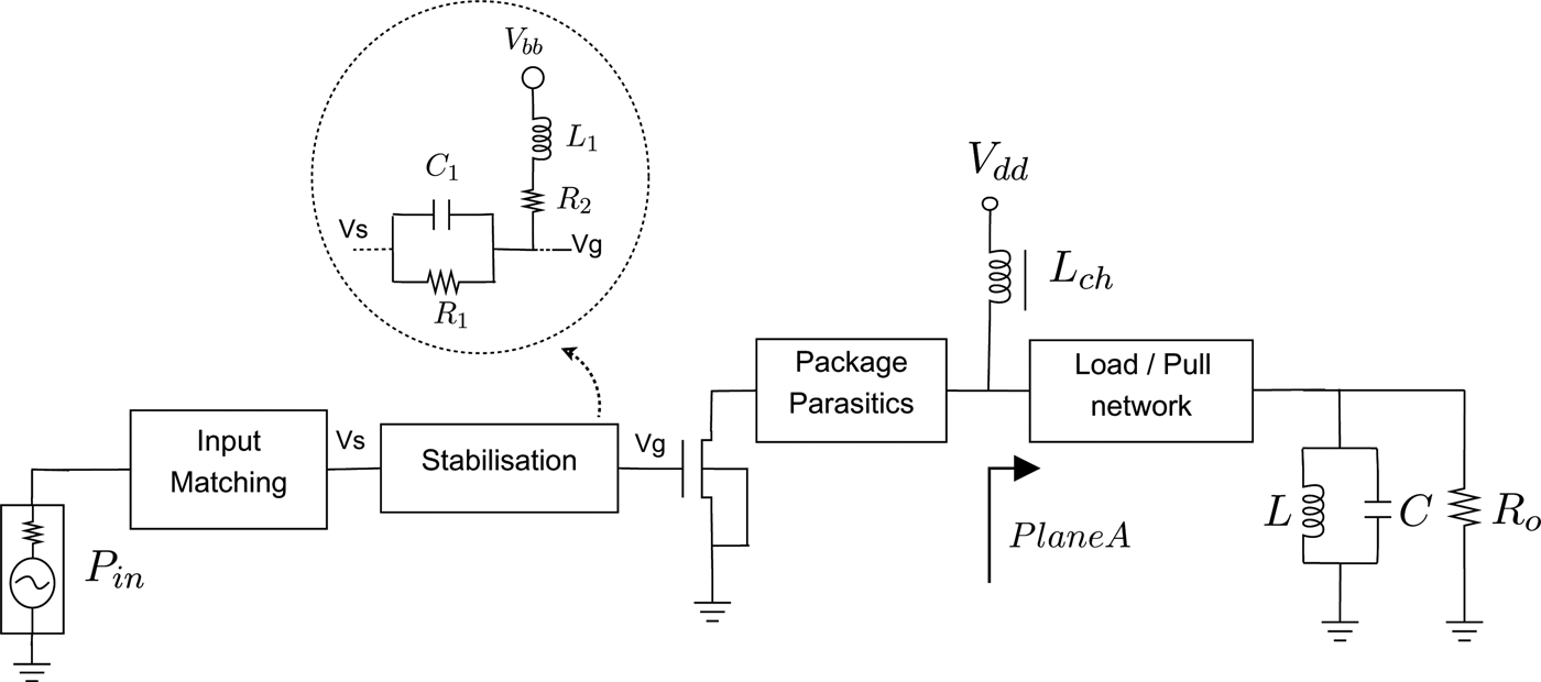
The design of classes AB, B, and C PAs follows the guideline given in [Reference Cripps11]. In order to attain the output power with a better efficiency, the conduction angle is set to α = 1.2π for the class AB PA and α = 0.85π for the class C PA. The design of the class J PA is based on the design of a class AB PA as explained in [Reference Cripps11, Reference Wright, Lees, Benedikt, Tasker and Cripps12]. The general topology for these PAs is depicted in Fig. 7 showing blocks of input matching, stabilization, and load pull network where the L-C network resonnates at the operating frequency. The transistor is unconditionally stable in wideband up to 10 GHz, thanks to the stabilization network [Reference Wood, Smith, Pribble, Pengelly and Crescenzi13]. By presenting optimal impedance with load pull network at plane A (Fig. 7) the maximal output power is transfered toward the output load R o. This value should be seen by each branch in the input of the Chireix combiner. Input matching network is designed to achieve an input impedance of 50Ω. For classes AB, B, and C, the drain current is roughly half-sinusoidal and the drain voltage sinusoidal except for class J whose drain voltage is also half-sinusoidal [Reference Wright, Lees, Benedikt, Tasker and Cripps12] as shown in Fig. 8.
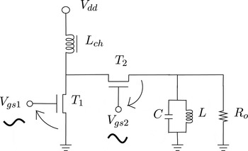
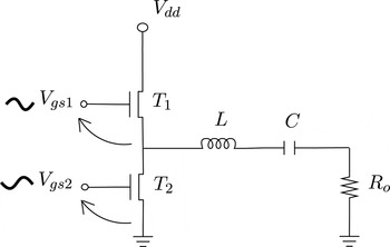
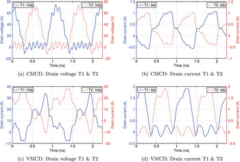
The design of operating classes PAs is based on the equations from [Reference Kazimierczuk14, Reference Grebennikov and Sokal15]. CMCD and VMCD PAs use two transistors in switched mode with outphased bias of gate–source voltage each one to other, see Figs. 9 and 10. In CMCD, drain current has a half-square wave while voltage is half-sine, whereas in VMCD, current is half-sinusoidal and voltage half-square, see Fig. 11.
Topology for class AB, B, C, and J PAs.
V ds and Ids curves simulated for classes AB, B, C, and J PAs.

CMCD power amplifier with parallel-resonant circuit [14].

VMCD power amplifier with a series-resonant circuit [14].

V ds and I ds curves simulated on both transistor for VMCD and CMCD.

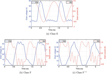
The class E is a switched mode PA with a specific output network made of a shunt capacitor connected to the drain of the transistor (in our case in the output at plane A) and a series L-C resonator [Reference Grebennikov and Sokal15]. Drain current has a half-sinusoidal fraction shape and drain voltage is slightly half-sinusoidal [Reference Kazimierczuk14, Reference Grebennikov and Sokal15] as shown in Fig. 13(a).
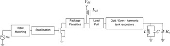
Classes F and F−1 PAs work with a biased transistor in class AB [Reference Kim16]. Shunt LC resonator circuits for odd (class F) or even (class F−1) harmonics are added in series to increase the efficiency and to give a square waveform to the drain voltage and drain current, respectively [Reference Raab17, Reference Kim16]. Topology for these classes is shown in Fig. 12 where each block, except for odd/even – harmonic tank resonators, behaves like in Fig. 7. Drain current in class F and drain voltage in class F−1 are half-sine, see Figs. 13(b) and 13(c). Harmonic manipulation approaches for second and third harmonic control for the design of these classes can also be considered (harmonic manipulated PA) [Reference Colantonio, Giannini, Leuzzi and Limiti18, Reference Colantonio, Giannini, Leuzzi and Limiti19]. Harmonic tank resonators for class F and F−1 were designed up to fifth and fourth hamonics, respectively [Reference Kazimierczuk14, Reference Grebennikov and Sokal15].
Topology for class F (with odd harmonics) and F−1 (with even harmonics) PAs.

Drain voltage and current for classes E, F, and F−1.

LINC architecture: Chireix combiner with compensation components and RF PAs.

PAE in LINC transmitter for each PA class.

B) Linearity and efficiency of the simulated PAs
Drain efficiency is computed for all classes of PAs. This efficiency is defined as the ratio between the active output power to DC power. The values obtained are shown in Table 1 and are slightly lower than theoretical values. PAs from operating classes exhibit the highest efficiency values, as expected.
Drain efficiency (DE) for the classes of RF PA designed.

Harmonic distortion (HD) is used to evaluate the linearity performance. HD is defined as the ratio between the power at the fundamental frequency and a given harmonic. Let us denote HD 2 and HD 3 for the second and the third harmonic distortion. The values obtained for all classes of PAs are shown in Table 2.
HD for the classes of RF PA designed.

We notice that class E and CMCD power amplifiers have the best efficiency performance with 88 and 83% drain efficieny, respectively. Also classes F and F−1 have the best linearity performance for HD 2 and HD 3, respectively.
V. LINC TRANSMITTER PERFORMANCES
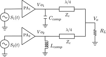
In this section we investigate the performances of the LINC transmitter designed with the previously presented PAs and the Chireix combiner. The circuit topology used for our simulations is depicted in Fig. 14. S 1(t) and S 2(t) represent two outphased power generators from equations (2) and (3). Vo 1 and Vo 2 represent the input voltages of the combiner at the upper and lower branches, respectively, and Vo is the output voltage. Values of C comp and L comp are taken from equation (14), Z c and R L are, respectively, the characteristic impedance of each quarter-wavelength transmission line and the output load of Chireix combiner. The analysis is conducted for two values of the compensation angle θcomp: 10 and 30°.
A) Global performances of the LINC transmitter
First, we characterize the transmitter with sinusoidal input signals, S 1(t) and S 2(t) in Fig. 14, as a function of the outphasing angle θ(t), i.e. S 1(t) and S 2(t) with positive and negative values of θ, respectively.
The overall PAE is calculated to analyze the impact of each class on the efficiency. This PAE is defined as follows:
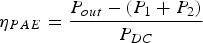
with P out the active output power delivered to the load R L, P 1, and P 2 the power at the input of the PAs and P DC the sum of the DC power consumed by the two PAs.
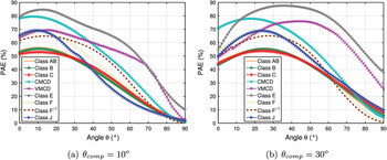
The PAE is plotted in function of the outphasing angle θ for two values of θcomp: Fig. 15(a) for θcomp = 10o, and Fig. 15(b) for θcomp = 30o.
Maximal PAE values are presented for each PA class in Table 3.
Maximum PAE for the different PA classes studied.

The maximum efficiency is obtained for the class E PA and for θcomp = 30o its efficiency remains above 80% for an outphasing angle between 15 and 60o. Among biased PAs, the class J has the best efficiency performance with a maximum value of 69% and remains above 60% up to an outphasing angle value of 30o. However, according to Fig. 5, the compensation of the Chireix combiner should have maintained a good efficiency performance over a widest range of the outphasing angle. For non-switched mode PAs one may notice that the value of θcomp has a lower impact than expected on this widening effect.
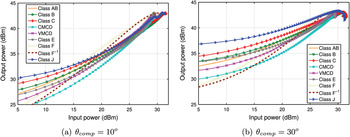
The linearity of the transmitter has been also studied with a 16QAM modulated signal. For this, we draw the equivalent AM/AM transfer function of the system, for each PA class, defined as the output power delivered to R L versus the theoretical input power of PAs calculated from the ideal sum of the two voltage signals: S 1(t) and S 2(t). These transfer functions are plotted in Fig. 16 using a 16QAM modulation for the two compensation angles, θcomp = 10 and 30o. Thus, the impact of each class of PA on the linearity of the whole system is observed.
AM/AM transfer function for all PA classes with a 16QAM modulation.

The analysis of these curves demonstrates that the compensation of the Chireix combiner modifies the linear behavior of the entire system: the lower compensation angle, the better the linearity. Only CMCD, class F−1 and class F PAs to a lesser extent, present an almost linear AM/AM slope close to unity. For the other classes, the AM/AM curves exhibit a distortion that is due to the unmatching effect of the combiner versus the outphasing angle, i.e. the load modulation effect. Indeed, the fact that the PAs do not have their optimum impedances at their outputs modifies both the amplitude and the phase of the transmitted signals S 1(t) and S 2(t). This results in a real outphasing angle lower than expected and so in a higher output power. Only a phase predistortion before the PA can compensate for this compression of the output power dynamic range. According to the PA class, this phenomenon has more or less impact. Unfortunately, the class E PA which presents the best efficiency is highly affected by this problem.
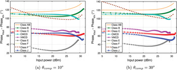
AM/PM transfer functions for all PAs are depicted in Fig. 17 for each compensation angle. These curves represent the difference of phases between the output and input voltages versus the theoretical input power of PAs as calculated in Fig. 16. Only class F PA presents a quasi-linear AM/PM curve for almost all levels of input power with a phase variation less than 5°. CMCD and class B PAs present a linear behavior between 15 and 25dBm of input power, whereas class F−1 and class E PAs are the most affected with phase variations up to 40 and 30°, respectively. Although the phase variations for class F−1 is significant, it is interesting to note that this class offers an acceptable linearity as will be shown by the results of the next section.
AM/PM transfer function for all PA classes with a 16QAM modulation.

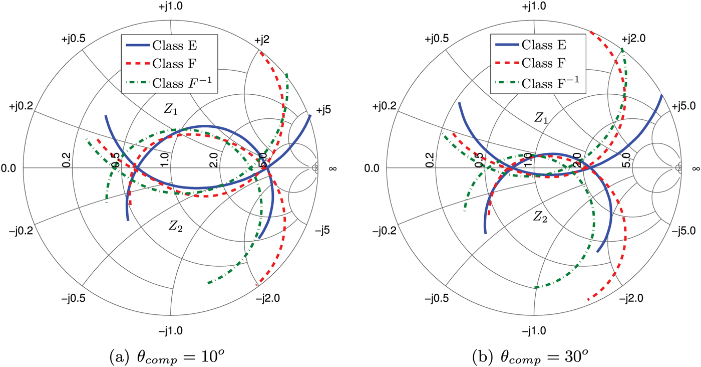
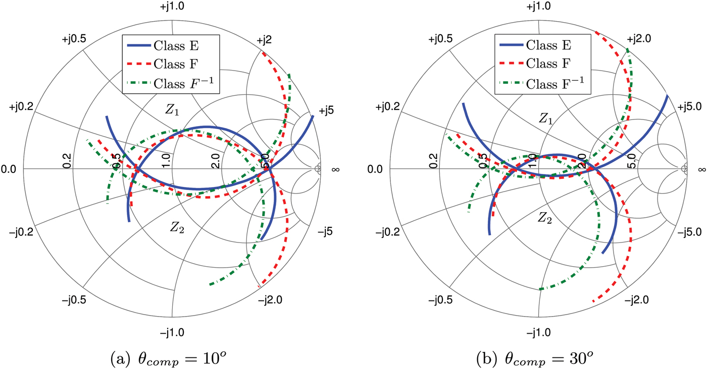
The distortion observed with AM/AM curves and AM/PM curves are linked to the load modulation effect. This load modulation effect is illustrated in Fig. 18 where the two load impedances presented to the PAs by the Chireix combiner are plotted in function of the angle θ and for three PAs classes: E, F, and inverse F. Z 1 and Z 2 are, respectively, the load impedances in the upper and lower branches of the LINC transmitter. The main point to note is that the impedances are not anymore complex conjugate. This is linked to the fact that the power transmitted by each PA do not results in voltages (V O1 and V O2 in Fig. 14) with the same amplitude and opposite angles as theoretically expected, thus impacting on the value of these impedances. We already highlighted that class E was highly affected by the load effect on the AM/AM and AM/PM curves. Here we can notice that the input impedances of the Chireix combiner are, for the class E, not at all complex conjugate and even more completely different from the ideal impedances presented in Fig. 6. This effect is less visible for the inverse F PA, resulting in more linearity.
Smith chart for classes E, F, and F−1 PAs. Z 1 and Z 2 represent, respectively, the impedances at the upper branch and lower branches (θ (0–90o)).
In the following section, we present the performances of the transmitter in terms of EVM, ACLR, and PAE using a 16QAM – modulated signal. These simulations are realized with θcomp = 30o that corresponds to the angle that gives the best efficiency.
B) Performances with a 16QAM – modulated signal
Simulations are carried out in this section using a 16QAM modulation with a 3.84 MHz symbol frequency and a roll – off equal to 0.35. As mentioned previously, the compensation angle used for the simulations presented here is set to 30o.
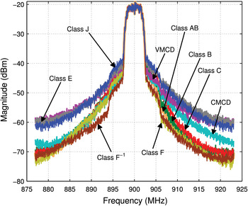
Figure 19 shows the spectrum at the output of the transmitter for all PA classes.
Output spectrum of 16QAM modulation with all classes of PAs.

EVM and ACLR values are shown in Table 4. ACLR is calculated with±5 MHz offset for the lower (ACLR1) and upper (ACLR2) bands.
EVM and ACLR for a 16QAM modulation.

These results confirm the observations mentioned in the previous section: CMCD, class F and F−1 PAs give the best linearity performance with an EVM lower than 7% and ACLR values higher than 25 dB.
The average PAE is calculated for the 16QAM modulation, see Table 5. The mean power for this modulation corresponds to a mean outphasing angle of 60o: classes F and F−1 present PAE values of the order of 40%. As predicted, the best efficiency for this modulation is obtained for the class E PA.
Average PAE (%) of a 16QAM modulation in LINC transmitter with all PAs.

VI. CONCLUSIONS
In this paper, we present a detailed comparative analysis of the LINC transmitter performances with different PA classes. This helpful understanding is represented and studied by equations, circuits, and simulations. A Chireix combiner is used for signal recombination in order to achieve high efficiency. Input impedances variation, i.e. load pull effect, of this combiner is due to the non-isolating behavior at the output of the PAs and affects substantially the overall performance. In this work, we demonstrate that this impact is highly dependent on the class of the PAs used and the compensation angle of the combiner as well.
Better efficiencies are achieved for class E, VMCD PAs but to the detriment of linearity with EVM values higher than 9%. On the other hand, the best choice in terms of linearity is the class F−1 PA with an EVM below 6% and an average efficiency of about 40% for a 16QAM modulation. Other choices to achieve a good linearity can be class F and CMCD. CMCD and VMCD require two transistors for their implementation, whereas the other classes require only one transistor.
The compression of the output power dynamic range is the main drawback of the use of a Chireix combiner. A predistortion of the outphasing angle appears to be a promising technique to alleviate this weak point. Such predistortion approach could allow to implement highly linear and efficient LINC transmitter using a Chireix combiner.
Some perspectives and upcoming works of this study are the implementation on Printed Circuit Board (PCB) and test of classes of PAs corresponding to the best trade – off between efficiency and linearity.
ACKNOWLEDGEMENTS
This work is realized within an European Catrene Project: PANAMA. We would like to thank Cree for providing their GaN HEMT model.
 Ronald Montesinos received the B.Sc. degree in electronic engineering from the National University of Engineering, Lima, Peru, in 2004. He received the B.Eng. degree in microelectronics and telecommunications engineering from Polytechnique School ofMarseille and the M.Sc. degree in wireless devices from University of Provence, Marseille, France, 2009. Since November 2009, he has worked toward his Ph.D. degree in Electronic and Micro-Nano electronic at electronic systems department of ESIEE Paris, Noisy-le-grand, France. His interest areas encompass RF power amplifiers, microwave components and circuts design, and RF transmitter architectures.
 Corinne Berland received the B. Eng. degree in electrical engineering from ESIEE Paris, Noisy Le Grand, France, in 1989, and the Ph.D. degree from the University of Marne La Vallée in 2001. From 1989 to 1998, she was with Alcatel Business Systemsand joined ESIEE Paris, in 1998, as an associate professor in the electronic systems department. She is now also with LaMips, Caen, France, for her research activities. Her main interests include transceiver architecture for radiocommunication systems and RF/analog – integrated circuits.
 Mazen Abi Hussein received the B.Eng. in electrical engineering from the Lebanese University, Beirut, Lebanon, in 2004, and the M.S. and Ph.D. degrees in electrical engineering from the polytechnique school of Nantes, France, in 2005 and 2009, respectively. From 2006 to 2009, he was with Thales, Cholet, France, as a research engineer, and he is currently a research engineer with ESIEE Paris, Noisy-le-Grand, France. His interests include wireless communications, nonlinear behavioral modeling, linearization techniques for high – power transmitters, and design of 3G transceiver architectures.
 Olivier Venard is an associate professor in Signal Processing and Telecommunication in the Telecommunication Department at ESIEE Paris, University Paris-Est since 1997. He conducts his research work in the LaMIPS laboratory. His interests are in the field of signal processing, digital communication, and digital software and hardware architecture.
 Philippe Descamps received the Ph.D. degree from the University of Lille, France, in 1992. From 1989 to 1999, he joined the research group Integrated Systems at the Institut d'Electronique, de Microélectronique et de Nanotechnologies (IEMN), Villeneuve d'Ascq, France, where he was involved in microwave research activities mainly guided by the characterization, simulation and design, and by the realization of field-effect devices in centimeters and millimeters wave ranges for automotive applications and telecommunication systems. In 1999, he became a full Professor at the Ecole Nationale Supérieure d'Ingénieurs de Caen (ENSICAEN), France where he currently heads the mixed research Laboratory of Microelectronics and Physics of Semiconductors (LaMIPS). He is mainly involved in high frequencies characterization, modelization of microwave components, and of the design of integrated circuits for telecommunication applications.