Semiconductor materials are grown in large slabs of crystalline material, so-called ingots, whereas industrial processes often require wafers, material slices of different thicknesses and surface qualities. The effort expended to create wafers is near that needed to create the material ingots in the first place. The fabrication of brittle semiconductor wafers is commonly realized using diamond or slurry-based wire sawing processes. These sawing processes result in kerf loss of potentially valuable material, surface roughness, and subsurface damage to the crystal. For microelectronic devices, the consequence of wire sawing is a need for additional polishing and grinding steps in the wafering process, causing further material losses and processing costs. For wafers sawn with the conventional processes about 50% of the material loss is due to the sawing process itself. The material loss for a 350 µm thick SiC wafer is about 300 µm for conventional processes, while the spalling processes presented in this work can reduce the loss to only 100 µm. This would lead to an increase of yield up to 33%.
In order to tackle the issues accompanying conventional semiconductor material wafering and thinning, kerf-free technologies have been developed that promise to decrease or maybe even to eliminate kerf-loss, subsurface damage, and polishing steps.[ Reference Henley 1 ] In particular, so-called spalling processes[ Reference Martini, Gonzalez, Dross, Masolin, Vaes, Frederickx and Poortmans 2 – Reference Bedell, Shahrjerdi, Hekmatshoar, Fogel, Lauro, Ott, Sosa and Sadana 4 ] use externally applied stresses—often thermally induced—to split crystalline materials along crystal planes with well-defined thickness. Spalling can be effected using nickel-chromium alloys,[ Reference Tanielian, Blackstone and Lajos 5 ] silver-aluminum pastes,[ Reference Dross, Robbelein, Vandevelde, Van Kerschaver, Gordon, Beaucarne and Poortmans 6 ] epoxy,[ Reference Martini, Gonzalez, Dross, Masolin, Vaes, Frederickx and Poortmans 2 ] aluminum[ Reference Niepelt, Hensen, Knorr, Steckenreiter, Kajari-Schroeder and Brendel 7 ] and nickel.[ Reference Bedell, Shahrjerdi, Hekmatshoartabari, Fogel, Lauro, Sosa and Sadana 8 ]
We have developed a spalling process that uses the differences in coefficients of thermal expansion between a brittle material and a polymer adhering to the material surface. Cooling the attached materials below the glass transition temperature of the polymer induces stresses that lead to lateral material separation. An additional benefit to this particular process in contrast to other types of spalling which are using enhanced temperatures[ Reference Dross, Robbelein, Vandevelde, Van Kerschaver, Gordon, Beaucarne and Poortmans 6 ] is that a reduced operating temperature inhibit diffusion processes of unwanted chemical elements through the material. Additionally, due to the low temperature, no dislocations will occur. Here, we demonstrate the process for 300 mm silicon substrates to show its favorable scaling with increased area.
Spalling processes, however, tend to be limited regarding the control of obtained wafer thicknesses,[ Reference Bedell, Fogel, Lauro, Shahrjerdi, Ott and Sadana 9 – Reference Niepelt, Hensen, Steckenreiter, Brendel and Kajari-Schröder 11 ] and adjusting the vertical position of crack propagation is complex. Furthermore, spalling creates a very prominent pattern of crack growth features such as Wallner and river lines on the surface due to the interaction of the crack front and transverse acoustic waves and changes in the multi-dimensional stress field during crack propagation.[ Reference Hull 12 ] These crack growth features allow the determination of crack growth direction and speed in the substrate. Typically, the crack propagates starting at some point on the edge, rapidly along the corner of the substrate.[ Reference Schoenfelder, Breitenstein, Rissland, De Donno and Bagdahn 13 ] The crack growth features from conventional spalling surfaces are causing a strong increase in surface roughness with the result of additional polishing or grinding actions are needed before the wafers can be processed.
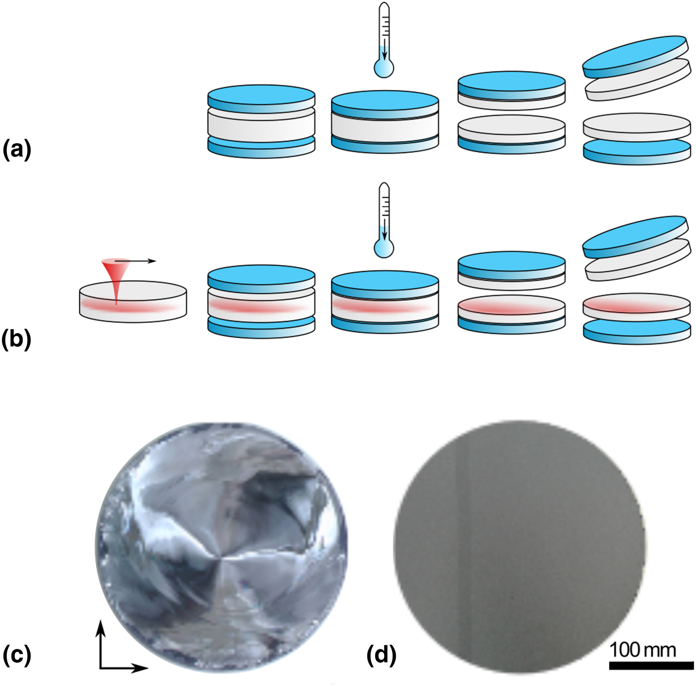
Figure 1(a) shows the standard procedure for laser-free spalling of large-area substrates. The wafer samples are usually used as-cut to avoid complications arising from rounded edges. Rounded edges are designed to prevent the onset of cracks at the wafer edges, which is detrimental to controlled crystal cracking along the lateral plane of the material. After standard cleaning procedures, the wafers are coated with a primer layer to enhance surface adhesion and a sacrificial layer to improve the polymer–wafer separation in the end. The wafer is then coated with a PDMS (polydimethylsiloxane) polymer foil of about 3 mm thickness attached via PDMS glue containing a platinum polymerization catalyst.
(a) Illustration of conventional spalling of solid substrates using an ensemble of two stress layers, i.e., polymer foils. The foils are attached on both sides of the substrate with a rapid cooling step to induce the spalling stress, followed by cracking and separation of spalled substrate and used foils. (b) Laser-assisted spalling process. In addition to the process steps shown in (a), a laser-conditioning step provides a structurally weakened layer within the material which defines a preferred plane for spalling crack propagation. (c) Image of one half of a 300 mm silicon wafer after separation using conventional spalling. Wallner lines are clearly visible as crack striations and indicative of high surface TTV. (d) Image of one half of a 300 mm silicon wafer after laser-assisted spalling. The surface is homogeneous with a mean surface roughness below 1 µm and no visible striations from crack propagation. The vertical line on the left side of the substrate is the result of table-limitations in the laser-conditioning process.

The samples are then pre-cooled to a temperature just above the polymer glass transition temperature before being immersed in liquid nitrogen. Dependent on size of the sample, up to 20 s later, the sample will have reached liquid nitrogen temperature. It is important to note that the system has reached thermal equilibrium at this moment. The semiconductor layers then separate in a spontaneously occurring spalling event. The spalling process is induced by the polymer glass transition, which has as a consequence a greatly increased Young's modulus in the polymer material. The additional difference in the coefficients of thermal expansion (CTE) between semiconductor and polymer then induces sufficient stresses to separate the crystal laterally. It should be noted that the process requires relative contraction of the polymer with respect to the semiconductor. Immersing the split semiconductor with attached PDMS foil in a separation bath eventually dissolves the sacrificial layer and allows recycling of the polymer as well as providing the wafered semiconductor for further processing steps.
As an answer to get rid of the crack growth features, we introduce a laser conditioning step prior to the spalling process, a method we term laser-assisted spalling (LAS). In this procedure, the lateral plane of crack propagation is defined through laser conditioning of the material using a combination of short laser pulses and high-numerical-aperture optics. The laser-conditioned layer is illustrated as a red area in Fig. 1(b) and will then define the plane of cracking separation in the spalling process. The laser photon energy is chosen below the material bandgap energy. In this way, the material is lucent to the conditioning laser, allowing deep penetration of the material. Through translation of the focusing optics along the optical axis, the plane of laser conditioning can be arbitrarily set and is defined through the focal plane of the focusing optics, which allows for single-micron-precision in both extent and position of the conditioned plane.
A typical resulting wafer surface from laser-free spalling is shown in Fig. 1(c). A pattern of crack growth features results from crack propagation inside the material. We observe surface striations—known as Wallner and river lines—which allow to track the cracking behavior along the plane of separation. Cracks arise at edges of the sample and propagate inward, generating a detailed pattern as shown in Fig. 1(c). The fourfold symmetry of the pattern is a consequence of the silicon fourfold crystal symmetry with a singularity or focal point of the meeting crack fronts at the center of the sample.
To compete the wire-sawing technology, however, the achieved surface quality is crucial for any spalling process. The resulting total thickness variation (TTV) of spalled surfaces without laser conditioning, commonly far exceeds industry demands. The TTV is on the order of 50 µm, which would require cost-prohibitive grinding steps before further processing. The LAS process has the potential to reduce the TTV significantly, which can be seen by surface roughness values of S a < 1 µm. The mean surface roughness S a is the extension of R a to a surface. It is calculated as the arithmetic average of the absolute values of surface coordinates z(x, y):
 $$S_{\rm a} = \displaystyle{1 \over A}\int {\int_{0,0}^{X,Y} {\left \vert {z(x,y)} \right \vert dxdy}} $$
and integrated over a sampled area A. The observed 1 µm roughness is comparable with wafer surfaces after standard lapping processes. The surface depicted in Fig. 1(d) exhibited a surface roughness of 670 nm.
Clearly, the laser modification step is crucial to the LAS process. A high numerical aperture (NA > 0.5) is required to confine the laser modification layer vertically. High NA optics lead to short Rayleigh ranges
 $$z_R = \displaystyle{{n\pi w_0} \over {\lambda _0M^2}}$$
with n as the refractive index of the material, w 0 as the beam diameter in the focal plane, λ 0 as the used laser's wavelength, and M2 as the beam quality parameter. Consequently, the highest laser intensity from focusing is also limited vertically to a thin sheet of few micron thickness. As the LAS process operates at wavelengths to which the material is transparent, high intensities are also needed to induce the required multiphoton processes at a significant rate. The probability of any multiphoton process scales with IN, where I is the laser intensity and N is the number of photons participating per event. According to this, the probability will scale most favorably for conditions with high instantaneous laser intensities, i.e. the use of pulsed lasers.
Pulsed lasers vary greatly in both average output power and pulse length, dependent on the technology they are based on. Typically, q-switched solid state lasers have nanosecond pulses, while pico- and femtosecond pulses (ultrashort pulses) require mode-locking. To achieve pulse energies suitable for material processing, ultrashort pulses require more elaborate amplification schemes in contrast to nanosecond pulses, so as to avoid damage to the amplification medium from exceedingly high instantaneous intensities.
In our experiments, a range of pulsed lasers was used, with pulse durations and pulse energies being individually fine-tuned for each material. Not all materials allow spalling without laser-conditioning, and materials that can be spalled without additional laser processing steps tend to be less demanding for pulse parameters such as pulse length.
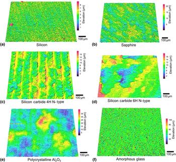
Figure 2 shows the set of materials that can currently be split using LAS with the relating surface topography from the roughness measurements. Three classes of material were successfully split: amorphous (Glass), polycrystalline (a variant of Al2O3), and crystalline (Si, SiC, Sapphire). The present understanding of spalling processes is that an initial crack is needed which travels along crystal planes. When dealing with polycrystalline or amorphous materials a lack of these circumstances is compensated by homogeneous structural modification via lasering. This allows crack-propagation in materials without defined crystal planes and hints at the universal applicability of the LAS process for the production of thin sheets of brittle material. The surface roughness measurements in Fig. 2 also illustrates how the resulting surface after separation is mostly defined by the laser process and partially by an interaction of laser process and crystal structure. It should be noted that silicon has the best surface roughness (S a = 0.79 µm) only because the process has been optimized the longest time in this case. Laser-assisted spalling of sapphire [Fig. 2(b)] leads to a surface roughness S a = 1.96 µm, while silicon carbide is currently spalled to surface roughnesses of S a = 2.22 µm [4H—Fig. 2(c)] and S a = 1.48 µm [6H—Fig. 2(d)]. The observed surface roughnesses after spalling from the non-crystalline materials of polycrystalline Al2O3 [Fig. 2(e)—S a = 3.93 µm] and glass [Fig. 2(f)—S a = 6.89 µm] indicate, however, that the presence of clearly defined planes is beneficial to the result. However, it should be noted that even for the spalling process without laser it is possible to use the {100} plane in silicon for cleavage, which is not one of the two preferential cleavage planes {110} or {111}. The silicon wafer had an initial thickness of 775 µm and was split in the {100} plane into 300 and 475 µm thick wafers. The SiC was split mostly from 360 µm initial thicknesses into the half, but also 700 µm of initial thickness is possible. Sapphire and glass were split into 250 µm thick samples and Al2O3 was split into 300 µm thick samples.
Overview of material surfaces after laser-assisted spalling. (a) Silicon surface split in {100} plane from the sample shown in FIG. 1(d), with a surface roughness of S a = 0.79 µm. (b) Sapphire (Al2O3) substrate surface (C-Plane) after laser-assisted spalling, exhibiting a surface roughness of S a = 1.96 µm. (c) and (d) Surfaces of silicon carbide polymorphs 4H and 6H (N-type doping) after laser-assisted spalling, with surface roughnesses of S a = 1.85 µm and S a = 1.29 µm, respectively. (e) Example of spalling of non-crystalline material, surface of polycrystalline Al2O3, with surface roughness S a = 3.89 µm. (f) Fused-silica, proof-of-principle experiment of laser-assisted spalling, with surface roughness of S a = 6.89 µm.

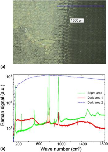
To further analyze the material modifications induced in the LAS process we subjected laser-treated material to Raman spectroscopy testing. Figure 3 provides a brief overview of the results for SiC of the 6H polytype, similar to what was done previously by Bedell and coworkers for spalled silicon.[ Reference Bedell, Fogel, Lauro, Shahrjerdi, Ott and Sadana 9 ] We find that several distinct phases can be found in the material after laser processing and that SiC forms a silicon and carbon phase, partially with an amorphous structure. Figure 3(a) is a microscope image of the SiC surface after spalling, with two different areas visible. A brighter and darker area can be discerned, the respective Raman spectra are plotted in Fig. 3(b). The peak strength (i.e., the signal intensity against the background) is reduced or vanishes completely in the darker area (red and blue curve), while they persist in the brighter area. We attribute this not only to increased amorphousness of the sample surface but also to different phases existing in the material. While the effect of peak strength reduction is most easily seen for the peaks at 765, 790, and 965 cm−1, the peaks around 265 and 500 cm−1 vanish completely in the darker areas, or are swallowed by an overall increase of the background between 130 and 510 cm−1. The structures around 1515 and 1720 cm−1 also vanish, hinting again at a structural change in the material from crystalline to amorphous. It is our interpretation of the data that the laser-induced amorphization observed here leads to a structurally weakened plane in the material that is energetically favored in crack propagation upon spalling.
Raman spectra from three different locations of spalled 6H silicon carbide. (a) Microscopy image of the surface after spalling. (b) Raman spectra from the darker area (on the right side in (a)) are red solid and blue dotted curves, with the green dashed curve as a Raman spectrum from the brighter area on the left in (a). The peak strength is reduced for darker areas for almost all peaks and at location 2 in the dark area, no Raman peaks whatsoever remain.
In order to study the influence of this laser-induced damage on the crack path during the spallation, a two-dimensional fracture mechanical simulation model was built, which is shown in Fig. 4(a). Here, a crack is modeled at the side edge as the starting point of spalling. The laser damage is modeled as openings in the material with a variation of tensile stress σ, representing a volume change due to laser damage. As criteria for planar crack growth, the coefficient of stress intensity factors for mode I (horizontal crack path) and mode II (kinking crack path) at the crack opening was used. The greater the coefficient, the less likely the crack will leave the horizontal (planar) crack path. In Fig. 4(b) the positive influence of the crack laser damaged area with increasing tensile stress can be seen by a high coefficient when the crack reaches the laser damaged area. Thus, the laser damage can be beneficial for processing planar crack surfaces and high wafer quality.
Fracture mechanical simulation of the influence of the laser-assisted spalling process on the crack path. (a) Half symmetrical model with a lateral induced crack with a laser damaged area loaded with varying tensile stress at material openings in front of the crack. (b) Coefficient of the stress intensity factor for mode I and mode II with variable loaded laser damage compared with a model without laser damage. The greater the coefficient, the less likely the crack will leave the horizontal crack path.

In conclusion, we have shown how laser treatment of solid substrates using short-pulse lasers and a high numerical aperture can significantly aid in the spalling of brittle materials. We have shown a dramatic reduction in TTV and surface roughness resulting from our laser-assisted spalling process. We have demonstrated that the LAS process allows spalling of amorphous, polycrystalline, and crystalline materials of varying bandgaps and material composition. Additionally, materials not capable of being conventionally spalled can be separated in a defined manner with separation layer thickness only defined through the laser process. While more demanding to implement than mere spalling, the LAS process is likely to be able to compete with conventional wire saws both commercially and technologically. Both the required laser sources and optics are already commercially available. We further anticipate that free-form surfaces can be defined from laser-modification at varying depth, opening new and unconventional options in material processing.