1. INTRODUCTION
Planar diodes, with explosive-emission cathodes, are widely used for the generation of wide-aperture pulsed ion and electron beams with a current density of more than 20 А/сm2. Studies have shown that after application of voltage to the diode and the formation of anode plasma, the generation of electron and ion currents occurs simultaneously, and the current density is limited by the space charge (Child-Langmuir limit (CL)) (Langmuir, Reference Langmuir1913). The current density of protons is 2.3% of the electron current density. The density of a heavier ion is lower. For effective generation of ion beams, it is necessary to ensure the suppression of the electronic component of the total diode current. In 1973, Sudan and Lovelace (Sudan & Lovelace, Reference Sudan and Lovelace1973) first suggested constructing a pulsed ion diode with applied magnetic insulation. The magnetic field causes the electron trajectory to bend (under the Lorentz force) by 90° (B > B cr) as the electrons drift across the electric field in the anode-cathode (A-K) gap (Dreike et al., Reference Dreike, Eichenberger, Humphries and Sudan1973). However, an additional energy source for the formation of the magnetic field increases the power consumption of the generator. For a total ion beam energy of 80–90 J per pulse, up to 500 J is required from the magnetic field source (Furman et al., Reference Furman, Stepanov and Furman2007). The efficiency of the generation of ion beam, taking into account the energy consumed to form the magnetic field, does not exceed 13–15%.
In 1977, Humphries (Humphries, Reference Humphries1977) first suggested the construction of an ion diode with self-magnetic insulation. A transverse magnetic field is formed in the A-K gap by the self-diode current when the current flows through the electrode. In this case, an additional magnetic field source is not required. This significantly simplifies the construction of the pulsed ion beam generator, but the efficiency of ion current generation in diodes with self-magnetic insulation does not exceed 5–10%, which limits their application.
The suppression of the electron component of the total diode current in the magnetically insulated diodes (applied or self-magnetic field) is possible to provide by increasing the electron transit time in the A-K gap. In the diode with applied magnetic field, it is easy to realize a closed electron drift in the gap, allowing them to drift perpendicular to the electric field lines during the whole voltage pulse. As a result, the efficiency of ion current generation in such diodes is more than 80% (Humphries, Reference Humphries1990). In the diodes with self-magnetic insulation, it is impossible to organize a closed electron drift, since one end of the electrode is grounded to the body of the diode chamber. The suppression of the electron current can be achieved either by reduction of their drift velocity or by increasing the length of the diode.
A study on the quasiplanar and quasipherical ion diodes with self-magnetically insulated electron flow was presented by VanDevender et al. (Reference Vandevender, Quintenz, Leeper, Johnson and Crow1981). The experiments were conducted using a Mite accelerator (2 MV, 400 kA, 35 ns). The ion current (protons) comprised 10% of the total diode current. The authors explain a low efficiency of ion current generation by a decrease in insulating magnetic field on the diode periphery. Different designs of diodes (VanDevender et al., Reference Vandevender, Quintenz, Leeper, Johnson and Crow1981; Bystritskii et al., Reference Bystritskii, Glushko, Kharlov and Sinebryukhov1991; Yoshikawa et al., Reference Yoshikawa, Masugata, Ito, Matsui and Yatsui1984; Remnev & Shulov, Reference Remnev and Shulov1993) with self-magnetic insulation can provide efficiency 10–13 times the CL limits. Our calculations show that in these diodes, the transit time of ions exceeds the electron drift duration in the gap; and their geometries do not provide a reduction of the electron component of the total current due to the insulating magnetic field. A detailed review of studies on diodes with self-magnetic insulation is given by Bystritski and Didenko (Reference Bystritski and Didenko1984), and in our papers (Pushkarev et al., 2009, 2010a, 2010b, 2011).
In spite of much progress in the development of intense ion beam sources, many processes in an ion diode with self-magnetic insulation have not been researched enough. In particular, no analysis of the mechanism of suppression of the electron current has been performed, nor have the reasons for the low efficiency been discovered. This can be explained in the following way: during the first 25–30 years, the main application of pulsed ion beams was in controlled thermonuclear fusion investigations. The production of ion beams with maximum current density and a pulse power of more than 1012 W were mostly attempted. This paper focuses on a theoretical and experimental study on the electron current suppression in different geometries of the self-magnetically insulated diodes.
2. EXPERIMENTAL SET-UP
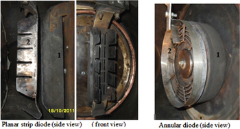
Investigations were conducted at the TEMP-4M accelerator (Remnev & Shulov, Reference Remnev and Shulov1993; Pushkarev et al., Reference Pushkarev, Tarbokov, Sazonov and Isakov2009) set in a double pulse mode: the first pulse is negative (300–500 ns, 100–150 kV) and the second is positive (150 ns, 200–250 kV). The beam is composed of C+ ions (80–85%) and protons; the beam energy density is 0.3–2.5 J/cm2 (for different types of diodes); the pulse frequency is 5–10 pulses per minute. The accelerator consists of the Marx generator, a nanosecond Blumlein line and a vacuum ion diode with self-magnetic insulation of the electrons. In the diode with self-magnetic insulation, the transverse magnetic field in the A-K gap is formed by a diode current flowing through the grounded electrode. For this purpose, it is grounded at one end only. We studied the strip planar diode (22 cm × 4.5 cm, A-K gap spacing of 8–10 mm) with a potential electrode made from graphite. Figure 1 shows a photograph of the planar strip diode and other geometry of the diode.
(Color online) Different geometries of planar self-magnetically insulated ion diodes: planar strip-diode and planar annular diode: (1) potential electrode (graphite), (2) grounded electrode.

The strip diode with self-magnetic insulation operated efficiently with the chamber pressurized to 0.1 Pa producing more than 107 pulses (10 years without breakage). The pulse repetition rate was limited by heating of the diode. The total diode current was measured using a Rogowski coil. The ion current density was measured by a magnetically insulated Faraday cup (0.4 T). The voltage on the potential electrode was measured by a high-frequency high-voltage divider that was installed in front of the diode connection. The electrical signals coming from the sensors were recorded with a Tektronix 3052B oscilloscope (500 MHz, 5 GSPS). A schematic of the TEMP-4M accelerator, diode connection, diagnostics and calibration can be found elsewhere (Pushkarev & Isakova, Reference Pushkarev and Isakova2012; Pushkarev et al., Reference Pushkarev, Isakova and Vakhrushev2010a).
3. EXPERIMENTS WITH THE PLANAR DIODE WITH SELF-MAGNETIC INSULATION
The majority of experiments have been done with the planar strip diode (Fig. 1). The potential electrode is made from graphite, and the grounded electrode from stainless steel. The grounded electrode has 30 slits, 4 mm wide and 5 cm long, resulting in a transparency of 60%. The gap spacing between the potential and grounded electrodes was chosen to match the diode impedance with that of the Blumline (4.5 Ohms). In the optimized arrangement, the gap increases from 8 mm at the bolted end of the grounded electrode to 10 mm at the open end.
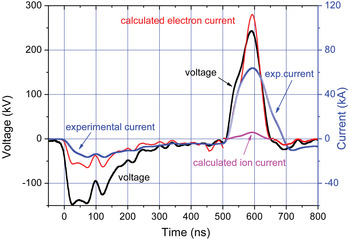
Some experiments were performed using a diode of a new design — an annular diode (Pushkarev & Isakova, Reference Pushkarev and Isakova2012). The photo of the diode is also shown in Figure 1. In this geometry, the potential electrode was made from a flat disc of graphite, 230 mm in diameter, and 40 mm thick. The grounded electrode is of a similar design to the previous one, except in this case, it consists of a stainless steel disc with a cutout in it. The outer diameter of the ring, or annulus, is 225 mm, and the inner diameter 125 mm. Again it is connected to the body of the diode chamber at one end (see Fig. 1). The average length of the annulus was 55 cm, which is 2.5 times greater than the length of the strip electrode in the planar diode. The area of the grounded electrode was 270 cm2. To increase the ion current density, we have designed a focusing annulus, which has a conical shape. Figure 2 shows typical waveforms which characterize the operation of the self-magnetically insulated diode.
(Color online) Waveforms of accelerating voltage, total current in the planar diode, and calculated currents of electrons and ions.

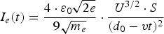
Figure 2 also shows the calculated values of both space charge limited electron and ion currents. The densities of space-charge limited electron and ion currents were calculated using the one-dimensional CL ratio, taking into account the reduction in A-K gap spacing due the plasma expansion. The electron current:
The ion current:

where U is the accelerating voltage; d 0 is the initial A-K gap; m e, М i is the electron and ion mass; e, Z is the electron and ion charge; S is the effective area of the potential electrode; v is the gap closure rate, t 0 is the time of the second pulse arrival (t 0 = 500 ns in Fig. 2), and α is the ion current enhancement coefficient.
On the second pulse, the bipolar flow is realized in the diode gap; therefore α = 1.86 was introduced to the ratio (Eq. (1)). When calculating the ion current it is necessary to take into account the effect of plasma erosion (Pushkarev et al., 2010b), which takes place in the A-K gap when the voltage reverses polarity, and also the effect of ion current density enhancement, which was observed in the self-magnetically insulated ion diode (Pushkarev et al., 2010a). To take the latter into account, the coefficient α = 6–8 was introduced to Eq. (2).
Our observations show that from the application of the voltage until a continuous plasma surface is formed on the potential electrode (the mode of discrete emitting surface, 0 < t < 200 ns in Fig. 2), the electronic component of diode current is limited by the emissivity of the cathode and is lower than the calculated CL value. After the potential electrode surface is covered with plasma (200 ns < t < 500 ns), the total diode current is limited only by the space charge of electrons in the A-K gap. Experimental values of the total current are satisfactorily described by the CL value obtained from Eq. (1) at a constant rate of gap closure equal to 1.3 cm/μs. During the second pulse (when the electron flow is inhibited by self-magnetic field), suppression of the electronic component of the total current by a factor of 1.5–2 occurs for the planar and focusing strip diodes. However, because the ion component does not exceed 10% of the total diode current (see Fig. 2), technical applications of the diode with self-magnetic insulation are limited.
As opposed to the diode with an external magnetic insulation in the ion diode with self-magnetic insulation, it is difficult to measure the induction, since the magnetic field is formed in the diode by current flowing though the electrode when a voltage of more than 200 kV is applied. The modeling and calculation of magnetic induction in the A-K gap was made using the Elcut software. Under our experimental conditions, the thickness of the electron sheath does not exceed 0.5 mm (Pushkarev et al., 2010a). The calculations show that at a distance of 0.5 mm from the plane of the grounded electrode, the magnitude of magnetic induction decreases by at most 10%. The skin depth on the grounded electrode, which is made of stainless steel, is 0.12 mm for a current frequency of 2.5 MHz (current pulse duration of 200 ns, see Fig. 2). The electrons in the skin layer and in the drift region during the second pulse move in one direction toward the open end of the diode. In this case, the magnetic induction in the A-K gap equals the sum of the magnetic field produced by the current through the grounded electrode and the magnetic field formed by the electrons drifting along the electrode; and varies slightly along the length of the diode. The magnitude of magnetic induction used for the calculation of the electron drift velocity was assumed to be constant over the length of the diode and equal the magnetic induction at a distance of 0.5 mm from the grounded electrode. When calculating the electron drift velocity one should take into account the reduction of the A-K gap spacing due to the plasma expansion and the effect of plasma erosion. The electron drift velocity v dr2 during the second voltage pulse is then

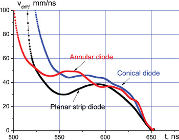
Figure 3 shows the drift velocity of electrons for different diodes with self-magnetic insulation. The experiments show that the electron drift velocity in the studied diodes with strip and annular geometry is 30–50 mm/ns. In the diode with an external magnetic insulation at a voltage of 300 kV, a gap of 5 mm, and induction of 0.8 T, the average drift velocity is 70 mm/ns (Furman et al., Reference Furman, Stepanov and Furman2007).
(Color online) The electron drifts velocity in the A-K gap for different diodes.

The electron transit time can be calculated as τ e(t) = l/(2·v dr2(t)), where l is the distance that electrons drift along the gap before they reach the anode plane. We used an average length of the cathode (l/2). Provided that ions are uniformly accelerated in the A-K gap, the maximum velocity that ions reach traveling across the A-K gap is ν max = a·τ ion. Hence, the transit time of ions in the gap τ ion (taking into account the reduction of the A-K gap and the effect of plasma erosion) is given by

where а is the acceleration in the electric field.
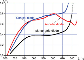
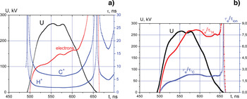
Figure 4 shows the relationship between the electron and C+ ion transit times in the A-K gap for the different diodes. The average length of the annulus in the focusing arrangement is 46 cm, compared with 55 cm in the unfocused arrangement, which is a factor of 2–2.5 times the length of the planar strip and focusing diodes. This leads to an increase in the transit time of electrons, which makes them drift in the A-K gap for longer in the annular diodes. However, because of the high drift velocity of the electrons, their transit time in the studied diodes still does not exceed the transit time of ions in the gap.
(Color online) The ratio of electrons to C+ ions transit times in the A-K gap for different diodes.

Studies show that in the strip diode, operating in a double-pulse mode, the plasma is formed effectively on the entire surface of the explosive-emission potential electrode (Pushkarev & Isakova, Reference Pushkarev and Isakova2012; Pushkarev et al., Reference Pushkarev, Isakova, Saltimakov and Sazonov2010a). During the generation of intense ion beam the condition of the magnetic insulation along the entire length of the diode (B/B cr ≥ 3) is fulfilled. However, the electrons have a higher drift velocity, so they will reach the anode plane much faster than carbon ions C+ and protons. This indicates a low efficiency of suppression of the electron flow in the strip and annular diodes. The increase in the efficiency of the ion beam generation from 0.7% (CL limit for C+ ions) to 9% is provided by the effect of ion current enhancement (Pushkarev et al., 2010a) and the effect of suppression of the electron emission due to the formation of the virtual cathode (Pushkarev et al., Reference Pushkarev, Isakova and Guselnikov2011).
4. THE STUDY OF THE SPIRAL SELF MAGNETICALLY INSULATED DIODE
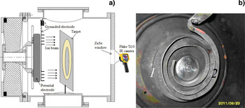
A new spiral geometry ion diode with self-magnetic insulation has been developed to improve the efficiency of the ion current generation. The schematic of the diode chamber, infrared imaging diagnostics for measuring the energy density distribution of the beam, and the photograph of the spiral diode are shown in Figure 5. The measurements of the spiral strip are an outer width of 16 cm, inner width of 7 cm, with a pitch of 1–1.5 cm, and a total length for the strip of 150–170 cm. The potential electrode is a flat disc of graphite, 20 cm in diameter, and 4 cm thick. The value of A-K gap spacing along the entire length of the diode was constant and equal to 7–7.5 mm.
(Color online) The schematic of the diode chamber, infrared imaging diagnostic (a) and the photo of spiral diode (b): potential electrode (1), grounded electrode (2).

The length of spiral grounded electrode was chosen to satisfy the condition that L > v dr·τ ion, where v dr, and τ ion are drift velocity of ions in the A-K gap and ion transit time, respectively. The distance between adjacent turns was selected so that h >2v·τ pulse where τ pulse is the duration of the second (positive) voltage pulse applied to the diode and v is the rate of cathode plasma expansion (equal to 1.3 cm/µs (Pushkarev et al., 2010b)) in order to prevent the closure of the gap between adjacent turns by expending plasma. Our expectation was that by increasing the length of the grounded electrode, we would increase the path along, which the electrons drift, making them travel in the A-K gap for longer before they reach the anode plane.
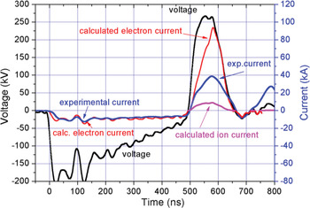
Figure 6 shows the waveforms characterizing the operation of the spiral diode in self-magnetic insulation mode and the calculated space-charge limited values of electron and ion current (obtained by Eqs. (1) and (2)). The area of the spiral electrode was calculated by

where L is the length for the strip, and Δ is the width for the strip (2 mm).
(Color online) Waveforms of the accelerating voltage, total current in the spiral diode, calculated current of electrons and ions.

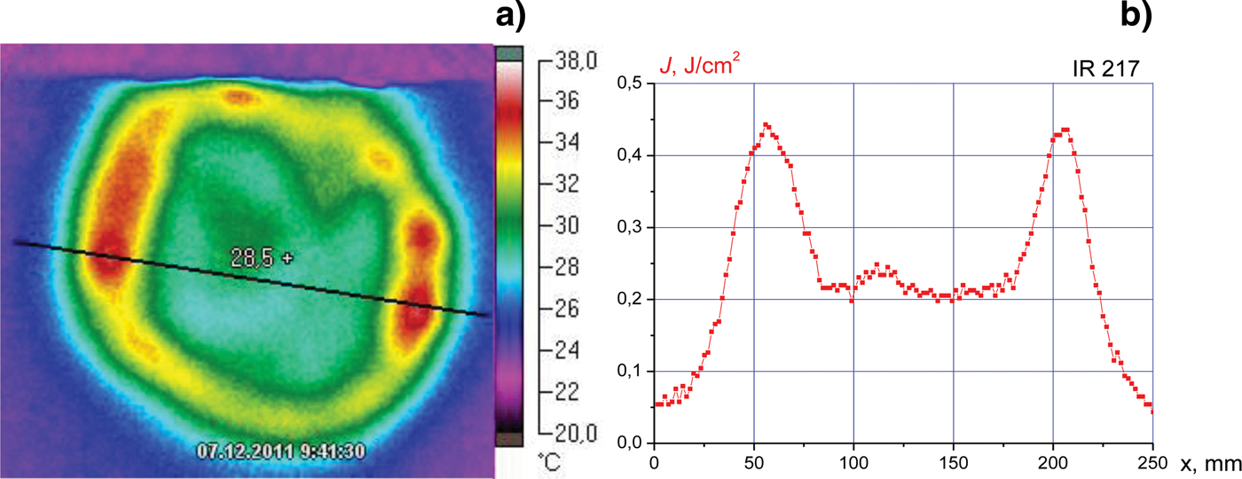
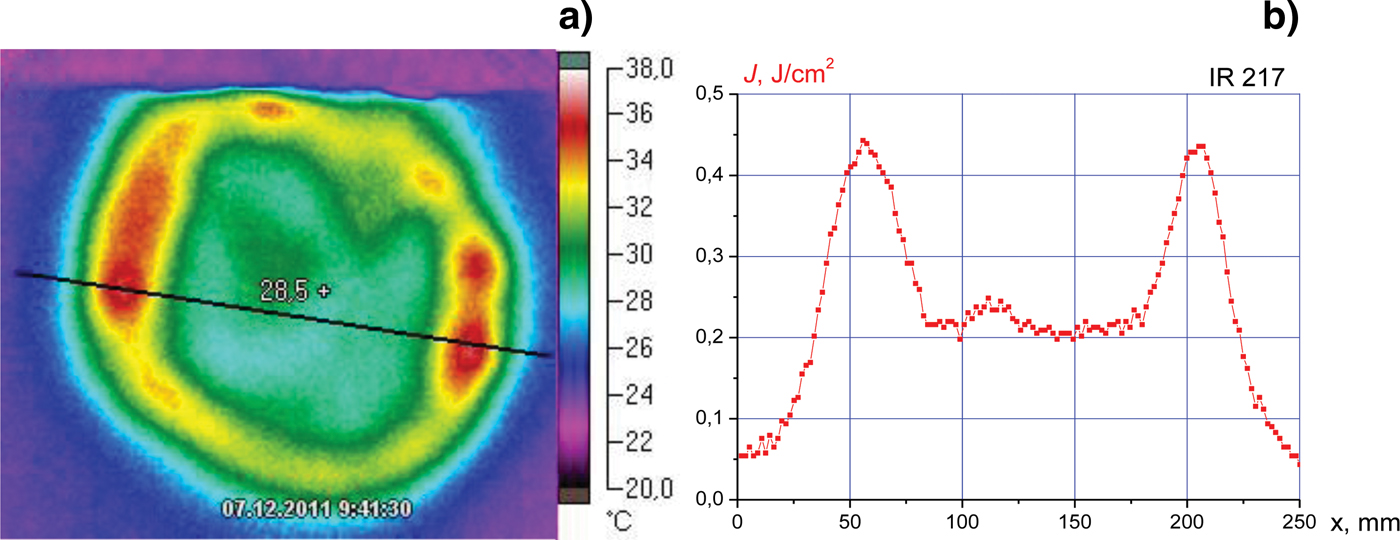
The ion beam in the spiral diode is uniformly generated over the whole area of the anode. We investigated the homogeneity of the ion beam generation using the infrared imaging diagnostic. Figure 7 shows a thermal imprint on the target intercepting the beam and the distribution of the energy density. As the target, a 100 µm stainless steel foil was used; the distance to the diode was 60 mm.
(Color online) Thermal imprint (a) and the beam energy density distribution in the horizontal section (b).
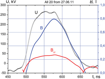
In the spiral diode, magnetic induction in the A-K gap during the second voltage pulse exceeds the critical induction 2.5–3 times (see Fig. 8). The calculation of the distribution of magnetic induction in the A-K gap was performed using the Elcut program at a distance of 0.5 mm from the grounded electrode surface, using the total diode current. We calculated the value of critical magnetic induction (Antonsen & Ott, Reference Antonsen and Ott1976) taking into account the reduction of A-K gap spacing (due to the plasma expansion) and the effect of plasma erosion:

(Color online) Waveforms of accelerating voltage, the magnetic induction in the A-K gap and the critical magnetic induction.

Figure 9a shows the calculated of values of the electron and ion transit times in the A-K gap during the second pulse for the spiral diode. The calculation was performed for singly-ionized carbon ions and protons. Figure 9b shows the relationship between electron and ion transit times.
(Color online) Waveforms of the accelerating voltage, transit time of C+ ions, protons and electrons in the A-K gap (a). The ratio of electron to ion transit times during the pulse (b).

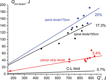
By increasing the length of the grounded electrode (cathode) in the spiral diode it seems possible to increase the electron transit time up to 10–15 ns, which is two times greater than that for C+ ions, and 7–8 times greater than the duration of the proton acceleration in the gap. In the spiral diode, the drift time for electrons in the A-K gap before they reach the anode plane is longer than in the other geometries of self-magnetically insulated diodes, which allowed us to increase the efficiency of the ion beam generation. Figure 10 shows the dependence of the total energy of the ion beam on the energy supplied to the diode from the Blumline line. The total ion beam energy (y-axis) was calculated by integrating the ion beam energy density distribution on the metal target intercepting the beam. Infrared imaging diagnostics were used to measure the thermal imprint caused by the ion beam hitting the target. The value of energy supplied to the diode from the Blumline line (x-axis) was calculated using the current-voltage characteristics of the diode. The current at the output of the Blumlein was measured using a Rogowski coil, the voltage was measured by using a voltage divider (the error doesn't exceed 10%).
(Color online) The dependence of the total energy of the ion beam on the energy supplied to the diode from the Blumline (points) in the planar strip and spiral diodes.

An additional effect that can reduce the value of the electronic components of the total current in the spiral diode is the reduction of the emission surface area of the grounded electrode compared to that of the potential electrode. At the time when the polarity of the accelerating voltage changes the area of emission surface equals the geometric area of the grounded electrode (cathode). Later, the area of emission surface increases as the plasma expands across the A-K gap. The area of emission surface of the grounded electrode does not exceed 50–60% of that on the potential electrode.
5. CONCLUSION
In contrast to the commonly used strip and annular ion diode with self-magnetic insulation, in the new spiral geometry it seems possible to reduce the electron component of the total current by means of the self-magnetic field. The electron transit time is greater than the ion transit time in the A-K gap. This leads to a significant increase in the efficiency of ion beam generation. The efficiency of ion beam generation in different diodes should be compared with the CL limit for a certain type of ions. This allows us to compare different geometries of the diodes from a standpoint of efficiency. Using the new spiral geometry diode it seems possible to provide an increase in the efficiency of C+ ion generation up to 17–20% according to our measurements of the beam energy density profile using an infrared camera. The spiral geometry of the grounded electrode provides a significantly higher transparency for ions and can increase the proportion of the beam extracted from the A-K gap into the transportation region by up to 80–90%. The ion beam is composed from carbon ions (80–85%) and protons, so the spiral diode provides an increase in the efficiency of C+ ion generation 25–30 times higher than the Childe-Langmuir limit. The electron component of the total current is decreased due to the following factors: the electron transit time exceeds the ion transit times in the A-K gap, the electron emission is limited by a virtual cathode, the area of emission surface of the grounded electrode is smaller compared to the potential electrode.
ACKNOWLEDGMENT
This work was supported by the Federal Program “Scientific and pedagogical personnel for innovative Russia”, SC P943 from May 27, 2010.