I. INTRODUCTION
Power dividers are widely applied in many communication systems, such as power-combining amplifiers, antenna array, mixer, and so on. In recent years, extensive power dividers have been proposed [Reference Chiu and Xue1–Reference Zhuge, Song and Fan13]. They are mainly focus on high isolation, dual-band response, and harmonic suppression, etc. The bandpass filter is another essential device of microwave circuits due to the ability of separating the desirable frequency band. Similarly, many bandpass filters have also been developed [Reference Mo, Song, Pan and Fan14–Reference Mo, Song and Fan19], including ultra-wideband (UWB) bandpass filters [Reference Wu and Chen20–Reference Shaman and Hong22] and multiple-band filters [Reference Mo, Song, Pan and Yong23–Reference Xu, Wu and Miao25]. Bandpass filters with high selectivity, small size, and strong roll-off in stopband are demanded in modern communication systems. Moreover, source–load coupling, mixed electromagnetic coupling, and special topology can be utilized to improve the frequency selectivity.
In addition, power divider and bandpass filter appear simultaneously in many microwave system. Integration of power divider and bandpass filter with ability to divide signals and bandpass filtering response can obtain lower insertion loss, small size, and low cost. Some power dividers with bandpass filtering response have been presented [Reference Shao, Huang and Pang26–Reference Li, Xue and Zhang31]. Grounded stepped impedance resonators are used to design the bandpass filtering-response power divider [Reference Shao, Huang and Pang26], and good frequency selectivity and small size can be obtained. In addition, two UWB bandpass filters are connected at the two output port, respectively, and UWB bandpass response and good frequency selectivity can be obtained in [Reference Wong and Zhu27]. However, its size is too large. In order to reduce the circuit size, the filters can be embedded at the two quarter-wavelength stubs of Wilkinson power divider [Reference Song, Mo, Zhuge and Fan28]. It can be seen that the filtering power dividers mentioned above are mainly focused on single band and UWB. But few research works about multi-band power dividers are presented.
In this paper, a compact tri-band filtering-response power divider is proposed. Two passband frequencies can be flexibly controlled by tuning the lengths of the stubs without disturbing the other one. The tri-passband characteristics are realized by properly controlling the lengths of the half-wavelength resonator and stubs. Meanwhile, five transmission zeros are generated, and good frequency selectivity can be obtained. According to even- and odd-mode analysis methods, the equivalent circuit of the proposed divider is presented and analyzed. The measured and simulated results show good agreement.
II. ANALYSIS OF THE SHORT/OPEN-STUB-LOADED RESONATOR
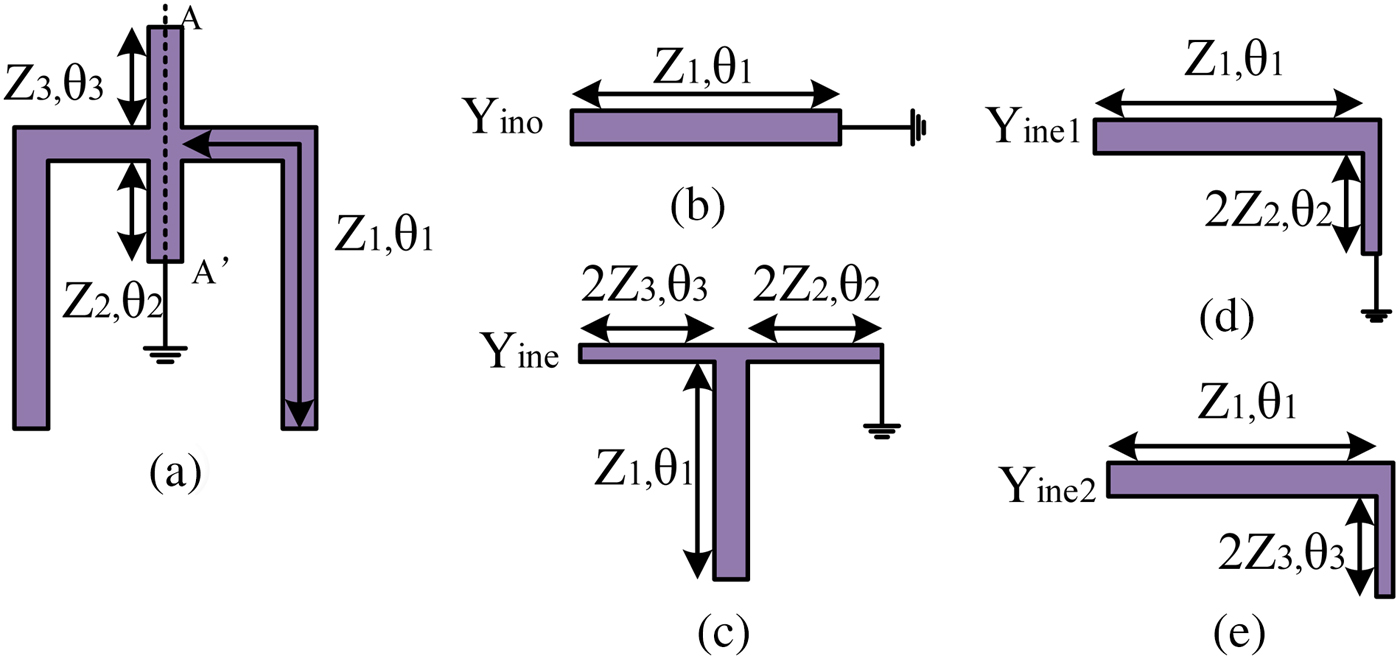
As shown in Fig. 1(a), the proposed resonator is a half-wavelength resonator with a short-stub and an open-stub shunted at the midpoint of the microstrip line, where Z 1 and Z 2 represent the characteristic impedances of the microstrip lines, and θ 1, θ 2, θ 3 denote the lengths of half-wavelength resonator, short stub, and open stub, respectively. Since the resonator is symmetrical to the A–A′ plane, it is convenient to analyze it by using the odd- and even-mode methods.
(a) Structure of stub-loaded resonator, (b) odd-mode equivalent circuit, (c) even-mode equivalent circuit, (d) λ/4 resonator of even-mode equivalent circuit, (e) λ/2 resonator of even-mode equivalent circuit.

For odd-mode excitation, the symmetrical plane is electric wall, and the equivalent circuit is shown in Fig. 1(b). The input admittance can be expressed as
 $$Y_{ino} = \displaystyle{1 \over {jZ_1 \tan \theta _1}}. $$
Under the resonance condition, Y ino = 0, then (1) can be deduced as
 $$\theta _1 = \displaystyle{{\lambda _o} \over 4} = \displaystyle{c \over {4f_o \sqrt {\varepsilon _e}}} \quad {\rm or}\quad f_o = \displaystyle{c \over {4\theta _1 \sqrt {\varepsilon _e}}}, $$
where c is the speed of the light in free space, and ε e denotes the effective dielectric constant of the substrate. It is demonstrated that the odd-mode resonant frequencies are not influenced by the stubs.
Under even-mode excitation, the symmetrical plane is magnetic wall, we can get the even-mode equivalent circuit (see Fig. 1(c)), which contains a quarter-wavelength resonator and a half-wavelength resonator. For the quarter-wavelength resonator (as shown in Fig. 1(d)), the input admittance can be obtain as
 $$Y_{ine1} = \displaystyle{{jZ_1 \tan \theta _2 + j2Z_2 \tan \theta _1} \over {Z_1 (2Z_2 - Z_1 \tan \theta _1 \tan \theta _2 )}}.$$
Under the resonance condition, then (3) can be deduced as
 $$Z_1 \tan \theta _2 = - 2Z_2 \tan \theta _1. $$
The half-wavelength resonator is shown in Fig. 1(e), the input admittance can be expressed as
 $$Y_{ine2} = \displaystyle{{Z_1 - 2Z_3 \tan \theta _1 \tan \theta _3} \over {jZ_1 (2Z_3 \tan \theta _3 - Z_1 \tan \theta _1 )}}.$$
Under the resonance condition, then (5) can be deduced as
 $$Z_1 = 2Z_3 \tan \theta _1 \tan \theta _3. $$
The resonators, as shown in Figs 1(d) and 1(e), can be considered as quarter-wavelength stepped impedance resonator (SIR) with one end grounded and half-wavelength SIR, respectively, and their resonance condition can be expressed as
 $$\tan \theta _2 = - 2\tan \theta _1, \quad {\rm when}\quad Z_1 = Z_2,$$
 $$1 = 2\tan \theta _1 \tan \theta _3, \quad {\rm when}\quad Z_1 = Z_3.$$
When θ 2 ≈ θ 3, we can obtain f e1 < f o < f e2 from (1)–(3). Thus, the first three resonant frequencies of the proposed stub-loaded resonator could be controlled by tuning θ 1, θ 2, and θ 3. The first resonant frequency is determined by θ 1 and θ 2, the second resonator frequency is determined by θ 1, and the third resonant frequency is determined by θ 1 and θ 3.
III. ANALYSIS OF THE TRANSMISSION ZEROS
The tri-bandpass filter structure will produce five transmission zeros. The five transmission zeros are named by TZ1, TZ2, TZ3, TZ4, and TZ5 from the left- to the right side. According to equations (3) and (5), if Y = ∞, each of them will produce one transmission zero. The condition can be expressed as
 $$2 = \tan \theta _1 \tan \theta _2, \quad {\rm when}\quad Z_1 = Z_2,$$
 $$1 = 2\tan \theta _1 \tan \theta _3, \quad {\rm when}\quad Z_1 = Z_3.$$
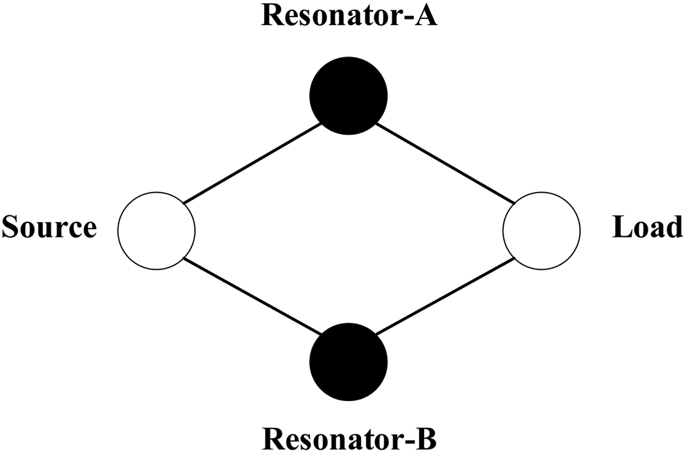
Because the tri-bandpass filter is composed of the two same tri-mode resonators, every passband can be regarded as single-bandpass filter composed of two same single-mode resonators. The topology of the proposed single-bandpass filter is shown in Fig. 2. This topology will produce one transmission zero. So, the tri-bandpass filter will produce three transmission zeros. In summary, the proposed structure will have five transmission zeros at all.
Topology of the proposed single-bandpass filter.

IV. DESIGN OF THE PROPOSED POWER DIVIDER
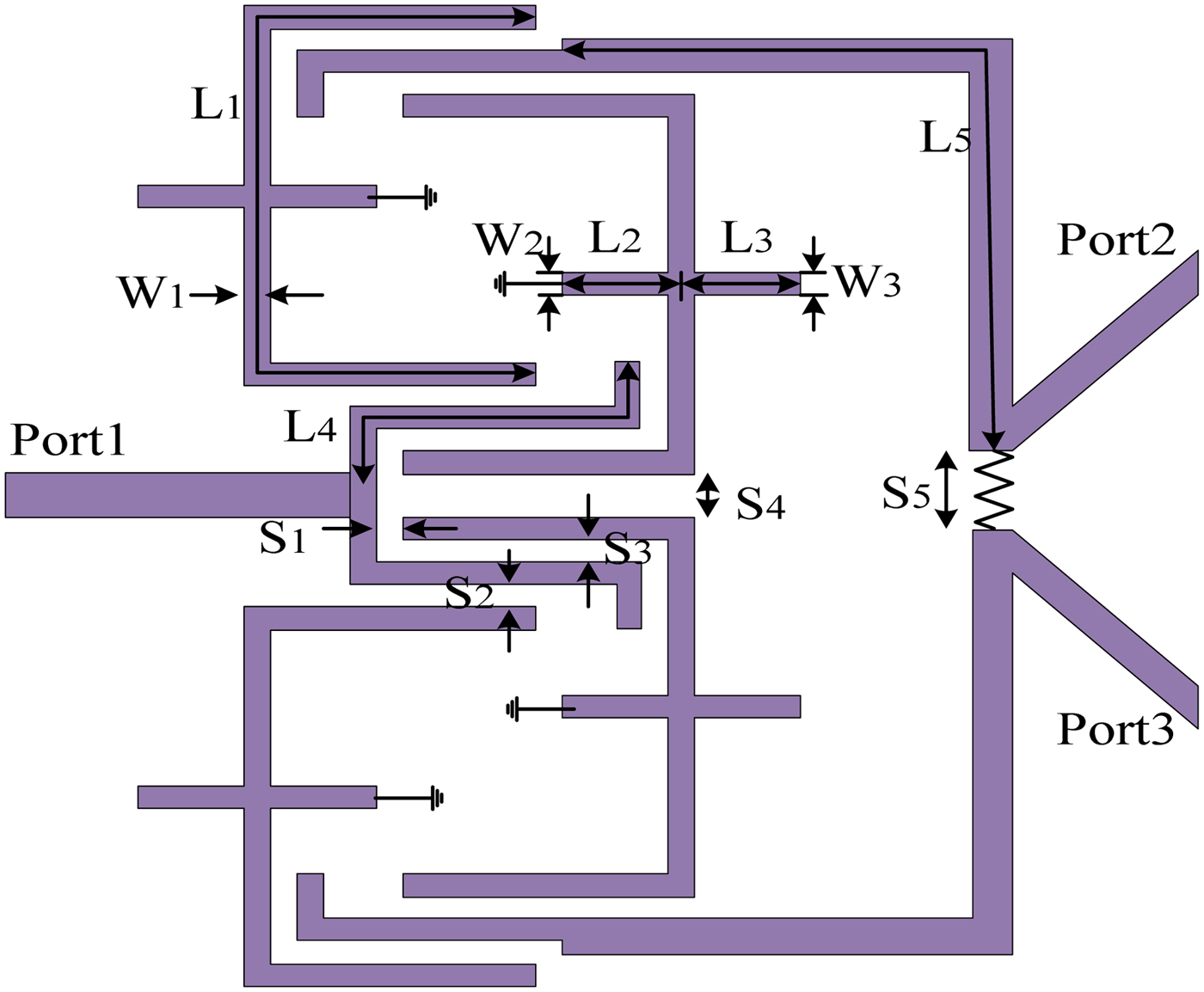
Based on the analysis above, the proposed resonator has three resonant frequencies and can be utilized to design tri-bandpass power divider. The configuration of the proposed tri-band power divider is shown in Fig. 3. There are two tri-band bandpass filters embedded in the presented circuit structure. A shunt isolation resistor R is located between the two output ports. Owing to the symmetric topology, it can be analyzed by using the even- and odd-mode methods.
Configuration of the proposed tri-band power divider.

A) Even-mode
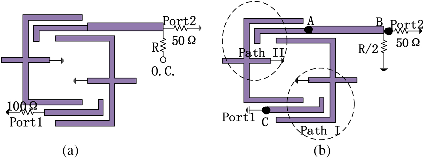
For the even-mode case, the even-mode equivalent circuit can be obtained and given in Fig. 4(a) when magnetic wall is applied to the symmetrical plane. Since the symmetrical plane is open circuit, there is no current flowing through the isolation resistor R; thus the isolation resistor can be considered invalid. Moreover, the characteristic impedance of input port 1 is 100 Ω.
Equivalent circuit: (a) even-mode, (b) odd-mode.

As can be seen, the even mode equivalent circuit is similar to that of an open-loop tri-band bandpass filter. It is demonstrated that the proposed power divider has tri-band bandpass filtering response because the bandpass filter is embedded in the power divider.
B) Odd-mode
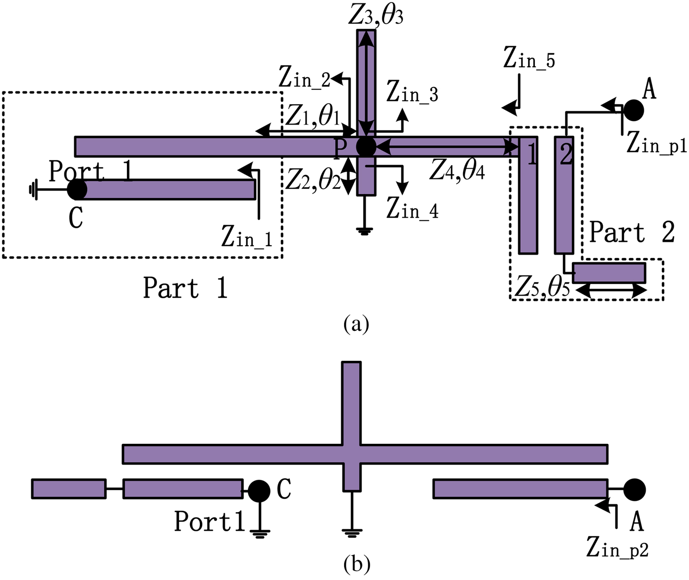
For the odd-mode case, the odd-mode equivalent circuit is given in Fig. 4(b) when electric wall is applied to the symmetrical plane. Since the symmetrical plane is short circuit, port 1 is shorted and the voltage along the middle of the isolation element is zero. Thus, the impedance of the isolation element is R/2. Under the odd-mode excitation, there are two transmission paths between two ports. Paths I and II are illustrated in Fig. 5. It can be seen that the even- and odd-mode equivalent circuits have the same structure between points A and C. It is convenient for the analysis of even- and odd-mode equivalent circuits.
Input impedance of the odd-even equivalent: (a) path I, (b) path II.

For part 1, the coupled line can be considered as a four-port circuit. As shown in Fig. 5(a), two of the ports are open circuit and another is shorted. Then, it becomes a one-port network. The input impedance of part 1 can be deduced as
 $$Z_{in\_1} = Z_{11}^{(1)} - \displaystyle{{Z_{14}^{(1)}} \over {Z_{11}^{(1)}}}, $$
where Z 11 (1) and Z 14 (1) are the Z-parameters of the parallel coupled line in part 1. Part 1 just can be considered as a load of the transmission line with characteristic Z 1 and electric length θ 1. Then the input impedance of this transmission line can be obtained
 $$Z_{in\_2} = Z_1 \displaystyle{{Z_{in\_1} + jZ_1 \tan \theta _1} \over {Z_1 + jZ_{in\_1} \tan \theta _1}}. $$
From node P to the open stub, the input impedance Z in_2 is
 $$Z_{in\_2} = \displaystyle{{Z_2} \over {j\tan \theta _2}}. $$
From node P to the open stub, the input impedance Z in_3 is
 $$Z_{in\_3} = \displaystyle{{Z_3} \over {j\tan \theta _3}}. $$
Then, the input impedance Z in_p from node P to the left part can be got
 $$Z_{in\_p} = Z_{in\_2} //Z_{in\_3} //Z_{in\_4}. $$
Also,
 $$Z_{in\_5} = Z_4 \displaystyle{{Z_{in\_p} + jZ_4 \tan \theta _4} \over {Z_4 + jZ_{in\_p} \tan \theta _4}}. $$
For part 2, it also can be considered as a four-port circuit. For simplifying the circuit analysis, the open-circuited microstrip line with length θ 3 is viewed as a capacitance in the equivalent circuit, where C 1 = tanθ 5/2πfZ 5. As shown in Fig. 5(b), one of the ports is opened and another is loaded with a capacitance. Then, it becomes a two-port network 1 and 2 are refined as the ports of the coupled line. The two-port elements of the impedance matrix are
 $$Z^{\prime}_{11} = Z_{11}^{(2)} - \displaystyle{{Z_{14}^{(2)} Z_{14}^{(2)}} \over {Z_{11}^{(2)} + X_1}}, $$
 $$Z^{\prime}_{12} = Z^{\prime}_{21} = Z_{13}^{(2)} - \displaystyle{{Z_{12}^{(2)} Z_{14}^{(2)}} \over {Z_{11}^{(2)} + X_1}}, $$
 $$Z^{\prime}_{22} = Z_{11}^{(2)} - \displaystyle{{Z_{12}^{(2)} Z_{12}^{(2)}} \over {Z_{11}^{(2)} + X_1}}, $$
where Z 11 (2), Z 12 (2), Z 13 (2), and Z 14 (2)are the Z-parameters of the parallel coupled line in part 2. Moreover, Z′11, Z′21, Z′12, and Z′22 are the new Z-parameters of the two-port parallel coupled line, and X 1 = 1/j2πfC 1.
According to the conversion between the transmission matrix ABCD and the impedance matrix (Z), the transmission matrix elements for the part 2 can be obtained. The input impedance of path I Z in_p1 is then calculated as follows:
 $$Z_{in\_p1} = \displaystyle{{AZ_{in\_5} + B} \over {CZ_{in\_5} + D}}.$$
Z in_p2 (input impedance of path II) can be obtained by using the similar method as that of Z in_p1. When Z in_p1 and Z in_p2 is obtained, the input impedance Z in can be calculated by using parallel of the two input impedances
 $$Z_{in} = Z_{in\_p1} \vert \vert Z_{in\_p2}. $$
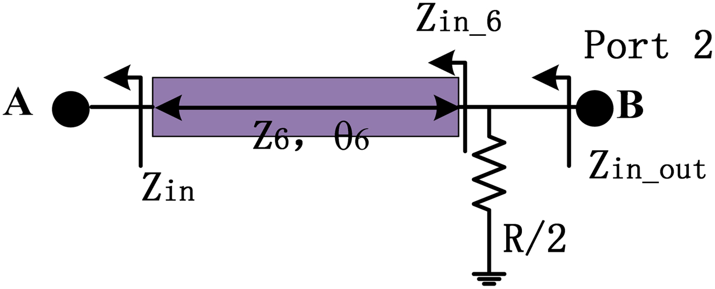
The equivalent circuit of the structure from A to B is shown in Fig. 6. Then, the input impedance of the transmission line with characteristic Z 6 and electric length θ 6 is
 $$Z_{in\_6} = Z_6 \displaystyle{{Z_{in} + jZ_6 \tan \theta _6} \over {Z_6 + jZ_{in} \tan \theta _6}}. $$
Equivalent circuit of the structure from A to B.

At port 2 (as shown in Fig. 6), it can be considered that the resistor of R/2 is parallel with Z in_6. After that, the input impedance Z in_p1 is calculated by using
 $$Z_{in\_out} = Z_{in\_6} //\displaystyle{R \over 2} = 50\;\Omega. $$
As a result, it is convenient to select R to get a good output match and isolation between the two output ports.
V. SIMULATION AND MEASUREMENT
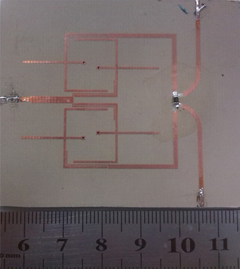
To verify and demonstrate the proposed tri-band power divider circuit, a tri-band power divider has been designed and implemented. A RF-35 substrate with a relative permittivity of 3.5, thickness of 0.508 mm, and loss tangent of 0.0018 is used. After simulation and optimization using HFSS, the dimensions of the fabricated tri-band filtering-response power divider are chosen as follows: L 1 = 37.5 mm, L 2 = 4.5 mm, L 3 = 11 mm, L 4 = 16.25 mm, L 5 = 34.45 mm, W 1 = W 2 = 0.6 mm, W 3 = 0.6 mm, S 1 = S 3 = 0.15 mm, S 2 = 0.3 mm, S 4 = 0.6 mm, S 5 = 1 mm. The photograph of the fabricated tri-band filtering-response power divider is shown in Fig. 7.
Photograph of the fabricated tri-band power divider.

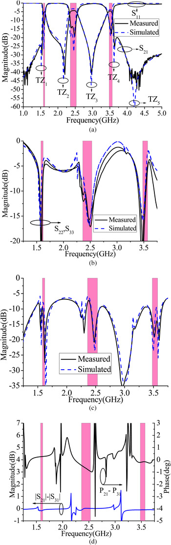
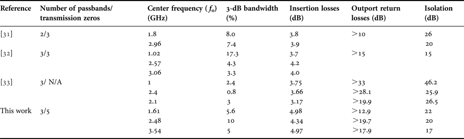
An Agilent 8757D network analyzer is used for measurements. The measured and simulated results are shown in Fig. 8. The measured 3-dB fractional bandwidths for the three passbands centered at 1.61, 2.48, and 3.54 GHz are found to be 5.6, 10, and 5%, respectively. The measured minimum insertion losses for the three passbands are 4.98, 4.34, 4.97 dB, and the return losses within the three passbands are 12.9, 19.7, and 17.9 dB, respectively. Moreover, more than 20 dB rejection levels within the lower stopbands, two middle stopbands, and upper stopbands are observed, featuring high out-of-band rejection level. In addition, five transmission zeros are located at 1.54, 2.2, 2.98, 3.64, and 4.25 GHz, respectively. These transmission zeros can improve the passband frequency selectivity and the out-of-band rejection level.
Simulated and measured results: (a) input return loss and insertion loss, (b) output return loss, (c) isolation, (d) phase difference and magnitude difference (pink frequency bands are the −10 dB frequency ranges).

Figure 8(b) presents the simulated and measured output return loss and the isolation between two output ports. It can be seen that the measured output return loss of the three passbands are more than 20, 16, and 15 dB, respectively. In addition, the measured isolation of the three passbands are greater than 22, 20, and 17 dB, respectively, as shown in Fig. 8(c). Meanwhile, the measured phase difference and magnitude difference between the output ports are less than 2° and 0.2 dB over the three passbands, respectively. The measured results show good agreement with the simulated ones. Slight deviation is observed, which could be attributed to fabrication tolerance in the implementation. Table 1 shows some reported performance of triple-band bandpass filters in recent years for comparison.
Comparison with some filtering-response power divider structures.

VI. CONCLUSION
A miniaturized tri-band filtering-response power divider with short- and open-stub-loaded resonators has been presented and developed. According to the characteristic analysis of the short- and open-stub-loaded resonator, the tri-passband response is realized by properly controlling the lengths of the half-wavelength resonator and stubs. The analysis theory and designed equations for the proposed tri-band power divider have been given. The simulated results are finally verified by the experiment of the fabricated tri-band filtering-response power divider.
ACKNOWLEDGEMENT
The work for this grant was supported by the National Natural Science Foundation of China (Grant No: 61271026).
 Zongrui He received the B.S. degree in Electronic Material from the University Electronic Science and Technology of China(Uestc) in 1999, the Master degree in Radio Physics is from Uestc in 2003, and the Ph.D. degree in Radio Physics is from Uestc in 2010. He is currently a deputy researcher of EE School at Uestc. He is currently involved with the design and fabrication of novel microwave and millimeter-wave circuits, high-power microwave and millimeter-wave modules, and application the modules to microwave and millimeter-wave circuits and systems.
 Kaijun Song (M'09–SM'12) received the M.S. degree in Radio physics and the Ph.D. degree in Electromagnetic Field and Microwave Technology from the University of Electronic Science and Technology of China (UESTC), Chengdu, China, in 2005 and 2007, respectively. Since 2007, he has been with the EHF Key Laboratory of Science, School of Electronic Engineering, UESTC, where he is currently a full Professor. From 2007 to 2008, he was a postdoctoral research fellow with the Montana Tech of the University of Montana, Butte, USA, working on microwave/millimeter-wave circuits and microwave remote sensing technology. From 2008 to 2010, he was a research fellow with the State Key Laboratory of Millimeter Waves of China, Department of Electronic Engineering, City University of Hong Kong, on microwave/millimeter-wave power-combining technology and ultra-wideband (UWB) circuits. He was a senior visiting scholar with the State Key Laboratory of Millimeter Waves of China, Department of Electronic Engineering, City University of Hong Kong in November 2012. He has published more than 80 internationally refereed journal papers. His current research fields include microwave and millimeter-wave/THz power-combining technology; UWB circuits and technologies; microwave/millimeter-wave devices, circuits and systems; and microwave remote sensing technologies. Professor Song is the Reviewer of tens of international journals, including IEEE Transactions and IEEE Letters.
 Bo Zeng was born in Sichuan, China, in 1993. He received the B.E. degree in electronic science and technology from the Chongqing University of Posts and Telecommunications, Chongqing, China, in 2015. He is currently pursuing the M.S. degree with the School of Electronic Engineering, University of Electronic Science and Technology of China, Chengdu, China. His current research interests involved with microwave circuits, including high efficiency and wideband power amplifiers.
 Yu Zhu was born in Anhui, China in 1992. He received his Bachelor of Engineering degree in Electrical Information Engineering from Southeast University Chengxian College in 2014, and now he is trying to obtain his Master degree in Electrical Engineering from the University of Electronic Science and Technology of China (UESTC). His current research interests include millimeter-wave techniques with a focus in RF/microwave passive.
 Yong Fan received a B.E. degree from Nanjing University of Science and Technology, Nanjing, Jiangsu, China, in 1985, and an M.S. degree from the University of Electronic Science and Technology of China, Chengdu, Sichuan, China, in 1992. He is a senior Member of Chinese Institute of Electronics. From 1985 to 1989, he was interested in microwave-integrated circuits. Since 1989, his research interests include millimeter-wave communication, electromagnetic theory, millimeter-wave technology, and millimeter-wave systems. He has authored or coauthored over 90 papers, 30 of which are searched by SCI and EI.