I. INTRODUCTION
The rapid growth of wireless communications has resulted in the proliferation of a large variety of new wireless components and sensors, ranging from mobile phones and personal digital assistant (PDA) to global position system (GPS) receivers and phased array radars, for which a transmit/receive (T/R) switch is one of the key elements. For most of these applications, low-loss/high-power RF switches are necessary, especially for multifunction antenna systems where a single aperture is used to serve multiple applications by simply switching between transmission and receive channels of the component.
The status on RF power switches today is that traditional p–i–n diode-based T/R switches encounter additional losses as a result of their intrinsic dc power consumption; on the other hand, the drive toward GaAs field effect transistor (FET)-based switches [Reference Gotch1] is hampered by the relatively low breakdown voltage of these components, requiring multi-stage design configurations with active device series connections to divide the maximum voltage of the input signal; pacing technologies based on wide-bandgap materials such as gallium nitride (GaN), because of their higher breakdown voltages, promise to extend the power level of the said microwave circuits by at least a factor of five and to appreciably reduce the overall chip size and cost. Apart from their exceptional power performance [Reference Meharry, Lender, Chu, Gunter and Beech2, Reference Micovic3], GaN high electron mobility transistor's (HEMTs) are promising candidates for robust low-noise applications due to their low-noise performance combined with their high power handling capability, providing major advantages in terms of linearity and robustness [Reference Krausse4]. Although some possibility for RF switching devices has been investigated, there have been few studies to date on the use of GaN HEMTs for high-power microwave and RF control applications [Reference Kaper, Thompson, Prunty and Shealy5–Reference Bettidi7]. The design of X-band and 2–18 GHz wideband monolithic microwave integrated circuit (MMIC) single pole double throw (SPDT) switches in microstrip GaN technology has already been presented in [Reference Ciccognani, De Dominicis, Ferrari, Limiti, Peroni and Romanini8, Reference Alleva9] and [Reference Alleva9], respectively: their performance in terms of insertion loss and isolation together with a preliminary nonlinear characterization of the switches have also been reported, demonstrating the promising power handling capability of such technology.
This contribution illustrates that GaN-HEMT microstrip technology is sufficiently mature for power switch applications. To this goal the design details of X-band and 2–18 GHz MMIC SPDT switches are given, together with a full on-wafer Pin-Pout characterization; power measurements have been performed with different control voltages on more than 10 samples for each circuit, demonstrating the good level of maturity reached in terms of fabrication yields and performance. This paper is organized as follows. In Section II, the AlGaN/GaN technology is briefly presented. The design approach and experimental results in terms of linear and nonlinear performance are shown in Section III for the X-band switch and in Section IV for the 2–18 GHz wideband switch.
II. DEVICE/CIRCUIT FABRICATION PROCESS
The SPDT switches reported below were fabricated with the current SELEX Sistemi Integrati GaN-HEMT Microstrip (MS) MMIC technology. The process is based on an epi-layer structure of GaN/AlGaN/GaN deposited on semi-insulating SiC substrates by either metalorganic chemical vapour deposition (MOCVD) or Molecular beam epitaxy (MBE) techniques. The mask levels for MMIC fabrication are based on a mix and match procedure utilizing both I-Line Stepper and electron beam lithography (EBL) processes. The latter is used only for the fabrication of the high-resolution quarter micron gate dimensions necessary for the HEMT devices. Drain and source electrodes of the devices are made by ohmic contact formation of a Ti/Al/Ni/Au metallization to the GaN/AlGaN epi-layer via a high-temperature alloying cycle. Wafer passivation for surface protection is carried out by SiN plasma-enhanced chemical vapor deposition (PE-CVD), while the active device isolation is achieved via fluorine ion implantation. The SiN passivation film deposition was optimized in order to minimize the carrier trap concentration at the interface with the semiconductor in order to minimize the detrimental drain dispersion phenomenon of the switch transistors.
After active device formation the MMIC fabrication process comprises the deposition of NiCr thin-film resistors, metal–insulator–metal (MIM) capacitors, and electro-plated inductors and interconnect transmission lines, with air bridges where necessary.
The fabrication process is concluded with back-side wafer processing for the fabrication of through substrate via-hole interconnects. The said process comprises wafer thinning down to circa 70 µm, via-hole etching by means of an inductively coupled plasma (ICP) dry etch process, and finally back-side (substrate and via-hole) metallization with a 10 µm thick electro-plated Au film deposited on an appropriate barrier metal layer.
III. X-BAND POWER SWITCH DESIGN AND PERFORMANCE
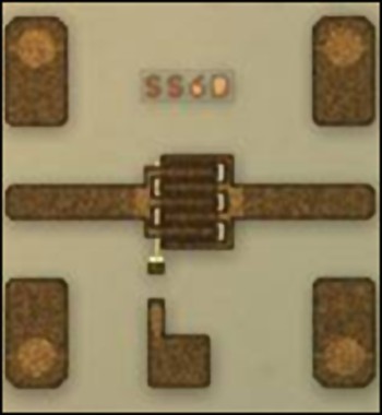
To design the microstrip X-band switch, S-parameter measurement on devices with layout itself in switching configuration were made in order to optimize the equivalent model extracted (Fig. 1).
Layout of the active device in switching configuration.

In particular, measurements on two devices with gate periphery equal to 600 µm (6 × 100 µm) and 300 µm (3 × 100 µm) were performed at different gate biases in cold FET conditions, and a model for on-state and off-state as a function of gate width was extracted.
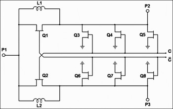
The design goal was to achieve an X-band switch with bandwidth 8–12 GHz, insertion loss better than 1 dB, isolation higher than 35 dB, and power handling at 1 dB compression (P1dB) greater than 5 W. The objective was to demonstrate that GaN-based switches can simultaneously achieve reasonably high power handling capability without sacrificing isolation and insertion loss. In order to satisfy these requirements, a circuit configuration, shown in Fig. 2, consisting of one series and three shunt transistors was adopted.
Circuit topology of the X-band AlGaN/GaN SPDT power switch.

To increase the isolation performance of the series devices (Q1 and Q2), an inductive (L1) compensation was implemented, as proposed in [Reference Ezzeddine, Pengelly and Badawi10]. When the transistor Q1 is in the ON state (i.e. ohmic mode), the inductance has no effect since it is in parallel with a low impedance and the switch insertion loss is not affected in the frequency band of interest. However, when Q1 is OFF (i.e. pinch off), it behaves as a large resistor (several thousand ohms) in parallel with a large capacitance; this parasitic capacitance reduces the isolation at high frequencies. To overcome this problem, the inductance L1 has been chosen to resonate at the upper side of the frequency band of interest so as to increase the isolation of the switch.
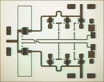
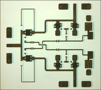
A micrograph of the fabricated SPDT switch, with overall dimensions 2.4 × 1.9 mm, is illustrated in Fig. 3.
Micrograph of the X-band MMIC SPDT switch.

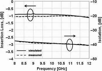
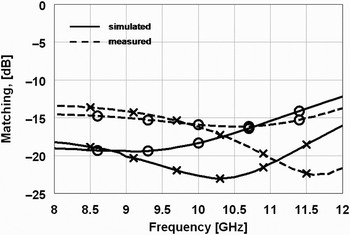
Small-signal performances of the X-band switch were evaluated by means of on-wafer measurements utilizing a vector network analyzer and related air-coplanar probes with orthogonal CPW SOLT calibration. Comparisons between measured and simulated results for insertion loss, isolation, and related port matching are presented, respectively, in Figs 4 and 5. As is evident, an excellent agreement between measurements and simulations was obtained. In particular, the insertion loss is equal to 1 dB and isolation is better than 37 dB in the whole bandwidth. The input and output port matchings are better than 13 dB.
Measured and simulated insertion loss and isolation for the X-band switch. Control voltage: V C = 0 V for insertion loss measurement and V C = −20 V for isolation measurement.

Measured and simulated port matching for the X-band switch (circles: S11; crosses: S22).

In order to demonstrate an overall on-wafer RF yield of the X-band switches within the above performance specifications around 65%, the repeatability of linear measurements made on all the chips of the 2-in wafer is illustrated in Fig. 6.
S-parameter measurements made on all the chips of the 2 in wafer showing an overall RF yield around 65%.

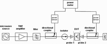
The on-wafer Pin-Pout characterization of the realized SPDT switches was performed using the setup illustrated in Fig. 7. The microwave source is a synthesized one (HP83640A), whereas a traveling-wave tube (TWT) amplifier (Hughes 8010H) is adopted to reach the required power level at the input of the device under test (DUT). The power levels at the DUT input and output ports are measured via two power sensors controlled by a power meter (Agilent E4418B). The narrow band-pass filter rejects the harmonic frequencies generated from the TWT amplifier, while the isolator increases the directivity of the input directional coupler. S-parameters of the probes were obtained using the unterminating method [Reference Bauer and Penfield11].
On-wafer setup adopted for the SPDT switch (DUT in figure) Pin-Pout characterization.

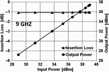
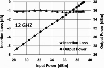
The Pin-Pout characteristics of the switch were measured between 8 and 12 GHz, in pulsed operation (duty cycle 25% and pulse width 100 µs). As shown in Figs 8 and 9, a very high power handling was measured at 9 and 12 GHz, respectively, where an input power equal to 39 dBm causes no compression phenomena. The input P1dB has not been reached due to limited test bench capability. Tuning the control voltage to −30 V, the input P1dB does not increase: this is due to the presence of the on-state switching series devices that cause a power compression phenomenon when the maximum RF current through the device exceeds the I dss.
X-band switch IL (triangles) and output power (circles) versus input power at 9 GHz. The control voltage is V C = −20 V.

X-band switch IL (triangles) and output power (circles) versus input power at 12 GHz. The control voltage is V C = −20 V.

IV. WIDEBAND POWER SWITCH DESIGN AND PERFORMANCE
The wideband SPDT power switch is based on the same transistor topologies and models outlined for the X-band version above. The switch was designed with a smaller series transistor, with gate periphery equal to 400 µm (4×100 µm), to achieve a low insertion loss in the entire bandwidth.
In this case, the design goal was to achieve a wideband switch with bandwidth 2–18 GHz, insertion loss better than 2 dB, isolation higher than 25 dB, and power handling at 1 dB compression (P1dB) greater than 5 W.
As illustrated in Fig. 10, a three-FET circuital topology was adopted, with the first device in series with the RF signal and the other two in shunt configuration. In this schematic the series HEMTs Q1 and Q3–Q4 are controlled by two control voltages C and C, one at zero gate bias and the other at a negative bias larger than the transistor pinch-off voltage.
Circuit topology of the wideband SPDT power switch.

Similar to the X-band circuit, the wideband design was performed using the compensation concept [Reference Ezzeddine, Pengelly and Badawi10]: in particular, a resistor R1 was added in series with the inductance L1. When Q1 is in the ON state, this series elements do not have relevant effects because it is in parallel with a low impedance and the switch insertion loss is not affected in the frequency band of interest. When Q1 is OFF (i.e. pinch off), the capacitance of the device resonates with the inductance L1. This resonance still reduces the capacitive effect near the resonance frequency and consequently increases the switch isolation; differently from the X-band design, the resistance has the effect of reducing the quality factor of the resonance to improve the positive effect introduced by the inductance for a wide band of frequencies. A micrograph of the fabricated wideband SPDT switch, with overall dimensions 2.0 × 1.7 mm, is illustrated in Fig. 11.
Micrograph of the 2–18 GHz MMIC SPDT switch.

Small-signal performances of the wideband switch were evaluated by on-wafer measurements, in a similar manner to the X-band switch reported above. Comparison of measured and simulated insertion loss, isolation, and port matching are, respectively, illustrated in Figs 12 and 13. As for the X-band circuit, the wideband switch exhibits excellent correlation between measured and simulated performances. In particular, measured insertion loss is lower than 2.2 dB in the overall bandwidth and isolation is higher than 25 dB. The input and output port matchings are better than 11 dB. The overall on-wafer RF yield of the wideband switches, within the above performance specifications, is around 65%.
Measured and simulated insertion loss and isolation of wideband switch. Control voltages: V C = 0 V for insertion loss measurement and V C = −20 V for isolation measurement.

Measured and simulated port matching for the wideband switch (circles: S11; triangles: S22).

To characterize the large-signal performances of the fabricated wideband switch, the setup illustrated in Fig. 7 was used. The Pin-Pout characteristics were measured between 2 and 18 GHz, with a CW input RF signal and a control voltage V C equal to −20 V. The input P1dB was not reached due to limited test bench capability, but the measured compression levels prove that P1dB is higher than 38.5 dBm in the entire bandwidth. In the worst case the switch exhibits a compression level around 0.3 dB in correspondence to an input power level of 37.5 dBm. In particular, Figs 14–16 illustrate the compression levels reached, respectively, at 4, 12, and 15 GHz.
WB switch IL (triangles) and output power (circles) versus input power at 4 GHz. The control voltage is V C = −20 V.

WB switch IL (triangles) and output power (circles) versus input power at 12 GHz. The control voltage is V C = −20 V.

WB switch IL (triangles) and output power (circles) versus input power at 15 GHz. The control voltage is V C = −20 V.

V. CONCLUSION
In this contribution the design, fabrication, and RF performance evaluation of high-power X-band and wideband 2–18 GHz switches have been reported.
The two MMIC SPDT switches, based on MS AlGaN/GaN HEMT on SiC substrate technology, demonstrated state-of-the-art performances with relatively good RF fabrication yields of about 65%. In particular, the X-band power switch demonstrated an insertion loss equal to 1 dB, an isolation higher than 37 dB, and a power handling capability better than 39 dBm at the 1 dB insertion loss compression point; the wideband switch showed an insertion loss lower than 2.2 dB, an isolation higher than 25 dB, and a power handling capability better than 38.5 dBm at the 1 dB insertion loss compression point in the entire bandwidth.
GaN-HEMT technology therefore demonstrates a good level of maturity for microwave power switch applications and as such is in a good position for the dedicated development of optimizing “switch transistor” technology and topology to specific applications.
ACKNOWLEDGEMENTS
This research activity was carried out in the KORRIGAN RPT N° 102.052 Project funded within the EUROPA framework in the CEPA 2 priority area. The authors wish to acknowledge the consortium members for their contribution and the European Defence Agency for its financial support.
 Ernesto Limiti is a full professor of electronics in the engineering faculty of the University of Roma Tor Vergata since 2002, after being research and teaching assistant (since 1991) and associate professor (since 1998) in the same university. His research activity is focused on three main lines, all of them belonging to the microwave and millimeter-wave electronics research area. The first one is related to characterization and modeling for active and passive microwave and millimeter-wave devices. Regarding active devices, the research line is oriented to small-signal modeling, noise, and large-signal modeling. For passive devices, equivalent-circuit models have been developed for interacting discontinuities in the microstrip, for typical MMIC passive components (MIM capacitors) and for waveguide/coplanar waveguide transitions analysis and design. For active devices, new methodologies have been developed for the noise characterization and subsequent modeling, and equivalent-circuit modeling strategies have been implemented for both small- and large-signal operating regimes for GaAs, GaN, SiC, diamond, Si, and InP MESFET/HEMT devices. The second line is related to design methodologies for nonlinear circuits. The main focus is on power amplifiers, frequency multipliers, and active mixers. Finally, the third line is in the development of extremely low noise amplifiers and receiving subsystems in general, including beam forming networks for active receiving antennas operated at cryogenic temperatures. The above research lines have produced more than 200 publications on refereed international journals and presentations within international conferences. Ernesto Limiti acts as a referee or editorial board member of international journals of the microwave and millimeter-wave electronics sector and is in the steering committee of international conferences and workshops. He is actively involved in research activities with many research groups, both European and Italian, and is in tight collaboration with high-tech Italian (Selex-SI, Thales Alenia Space, Rheinmetall, Elettronica S.p.A., Space Engineering, etc.) and foreign (OMMIC, Siemens, UMS, etc.) companies.
 Andrea Bettidi received an electronic engineering degree from the University of Roma Tor Vergata, Rome, Italy, in 1999. From 2001 he has been working in SELEX Sistemi Integrati S.p.A., where he has been involved in the design of monolithic microwave integrated circuits (MMICs). His current research interests include the development of MMIC chip sets for state of-the-art transmit/receive front ends.
 Walter Ciccognani was born in Rome, Italy, in 1977. He received an electronic engineering degree in 2002 and a Ph.D. degree in 2007 from the University of Roma Tor Vergata, Rome, Italy. He is currently working in collaboration with the University of Roma Tor Vergata. His main research activities are in the field of linear microwave circuit design methodologies, linear and noise analysis/measurement techniques, and small signal and noise modeling of microwave active devices.
 Marco De Dominicis was born in Rome, Italy, in 1972. He received an electronic engineering degree and a Ph.D. degree in microelectronics and telecommunications from the University of Roma Tor Vergata, Rome, in 2000 and 2004, respectively. During his research activity, he was involved in noise characterization and modeling of microwave and millimeter-wave active devices. From 2004 he has been with Elettronica S.p.A., Rome, Italy, as a senior microwave engineer, where he is involved in the design of microwave and millimeter-wave modules for EW systems. His current research interests include the design and testing of AlGaN–GaN-based MMICs.
 Marco Peroni was with SELEX Sistemi Integrati S.p.A. (formerly AMS) till 1990 as a process engineer at the GaAs Foundry. During his work activity he was involved in process development, characterization, reliability issues study, as well as modeling of III–V microwave devices, and in these topics he has contributed with numerous papers and presentations for international technical magazines and congresses. At the moment he is primarily involved in GaN HEMT and GaAs PIN diodes devices development, and is responsible for Selex S.I. activity in several national and European research programs.
 Vincenzo Alleva was born in Rome in 1956 and received an electronic engineering degree in 1982 from the University of Rome “La Sapienza”. He also attended the Scuola di specializzazione in Elettromagnetismo Applicato in the same year. In 1983, he joined SELENIA S.p.A. and worked in the Microwave Laboratory of the Development Directorate. During the 8 years spent in the department, he was involved in the following programs: 3D long range radar, ATC radars (Matcals, Europa 2000), and radar for EFA. His development interests included microwave and millimeter wave, semiconductor devices, passive circuits, and microwave components. His research interests also included MMIC design. In 1991, he joined Itelco SpA in Orvieto as manager of microwave and system departments. Itelco is involved in broadcasting and telecommunications. During this period he worked on a transmitter for broadcasting using IOT In 1992, he was the organizer of the 1992 International Workshop on Millimeter Wave sponsored by IEEE in Orvieto. In July 1992, he joined Elettronica S.p.A. and was responsible for the microwave department. This department has a high capability in the design of super-components integrated with MIC and MMIC. In September 1996, he joined Alenia Spazio and was responsible for the microelectronic department in the L’Aquila plant. Then he was appointed as product manager of power transmitter and microwave channel amplifier for commercial satellites in USA (Lokheed Martin). During this period he was also product manager for international mission and programs such as Rosetta and Mars Express. From November 2000, he joined Telital Uni.Com Centro Ricerche as laboratories in charge. Telital Uni.Com Centro Ricerche is a research and development center, fully dedicated to radio-frequency and millimeter-wave systems research and development. In June 2003, he joined Elettronica S.p.A. as program manager. In January 2008, he became responsible for hardware design laboratories of the same company. Developments of antennas, microwaves, signal process, and power supply activities belong to this operative unit.
 Mauro Ferrari was born in Rome, Italy, in 1981. He received a B.Sc. degree and an M.Sc. degree in electronic engineering from the University of Roma Tor Vergata in 2003 and 2006, respectively. He is currently persuing the last year of the Ph.D. course in telecommunications and microelectronics engineering at the same university. His research interests are mainly in the field of analysis and design of advanced microwave and millimeter-wave MMICs developed on GaAs, GaN, and novel high-performances materials.