I. INTRODUCTION
In recent years, there has been an increasing demand for transparent conductors. The growth in demand is anticipated to persist as optoelectronic devices and components, which utilize transparent conductors, become ubiquitous in our lives. Some of these devices include panel displays, touch panels used in tablet personal computers and smart phones, light-emitting diodes, and photovoltaic cells.
Films made from doped metal oxides, especially indium tin oxide (ITO),Reference Mizuhashi1, Reference Kim, Gilmore, Pique, Horwitz, Mattoussi, Murata, Kafafi and Chrisy2 are commonly used as the transparent conductors. Besides good electrical conductivity and optical transparency, the production of ITO films can be scaled up. However, ITO has several drawbacks. ITO is very brittle and can crack and fracture at relatively low strains,Reference Cairns, Witte, Sparacin, Sachsman, Paine, Crawford and Newton3 which limits its integration in flexible devices, an emerging area of electronic and optoelectronic systems. A component material of ITO, indium, is very expensive due to its scarcity. Production of ITO films via costly vacuum deposition technique also drives the cost of ITO films up. Hence, many research groups have explored various alternatives to ITO.
Alternative metal oxidesReference Minami4–Reference Yang and Forrest6 were considered but they also suffered the similar drawback of brittleness. Nanomaterials such as carbon nanotubes (CNTs),Reference Hu, Hecht and Gruner7–Reference Hecht, Heintz, Lee, Hu, Moore, Cucksey and Risser12 graphene,Reference Li, Zhu, Cai, Borysiak, Han, Chen, Piner, Colombo and Ruoff13–Reference Bae, Kim, Lee, Xu, Park, Zheng, Balakrishmam, Lei, Kim, Song, Kim, Kim, Ozyilmaz, Ahn, Hong and Iijima17 and metal nanowiresReference Hu, Kim, Lee, Peumans and Cui18–Reference Wu, Hu, Rowell, Kong, Cha, McDonough, Zhu, Yang, McGehee and Cui21 were also examined. However, it remains challenging for any of these materials to approach sheet resistance of ∼10 Ω/□ and transmittance of ∼90%, which is achievable for ITO. Films of CNTs and metal nanowires are not able to attain very low sheet resistance while maintaining high optical transmittance because of the presence of junction resistance between the nanotubes or nanowires.Reference Hu, Hecht and Gruner7, Reference Nirmalraj, Lyons, De, Coleman and Boland10 Graphene films produced via scalable solution processes tend to have fairly low mobility, which also results in higher sheet resistance relative to ITO.Reference Eda, Fanchni and Chhowalla22, Reference Tung, Allen, Yang and Kaner23
A hybrid transparent conductor that integrates a thin metal grid and graphene film was developed recently.Reference Zhu, Sun, Yan, Jin and Tour24 It demonstrates a sheet resistance and transmittance comparable to ITO: ∼20 Ω/□ at 90% transmittance. This hybrid transparent conductor possesses both the attributes of its component materials. The graphene film is chemically and thermally stable and can potentially form a barrierReference Bunch, Verbridge, Alden, van der Zande, Parpia, Craighead and McEuen25, Reference Chen, Brown, Levendorf, Cai, Ju, Edgeworth, Li, Magnuson, Velamakanni, Piner, Kang, Park and Ruoff26 to prevent the degradation of the metal grid when exposed to the environment. The metal grid with large clear aperture (i.e., percentage of surface not covered by the metal grid lines) displays both high optical transparency and electrical conductivity. As the metal grid is formed from a metal thin film, which is defined via photolithography, the metal grid lines that cross one another form a continuous electrical pathway, unlike metal nanowires deposited on a substrate. This is very crucial because it eliminates junction resistance and thus lowers sheet resistance immensely. The graphene provides a continuous conducting film that “fills up the voids” in the metal grid. This is essential when the transparent conductor is applied in photovoltaic cells. Both metal grid, if sufficiently thin, and graphene film are mechanically flexible, which makes them suitable for integration in flexible devices. Furthermore, the electrical and optical properties of this hybrid transparent conductor can be easily tuned by designing the metal grid. We will examine the important parameters in the design of the metal grid and investigate the thermal stability of the hybrid transparent conductor in this paper, which were not studied in previous work.Reference Zhu, Sun, Yan, Jin and Tour24 This provides useful insight for the optimized design of a stable transparent conductor that can potentially be used in applications requiring high transparency, electrical conductivity, and thermal stability.
II. EXPERIMENTAL
A. Synthesis of graphene
Thin copper foils (25-μm thick and 99.8% purity) were purchased from Alfa Aesar (Ward Hill, MA). The foils were loaded in a reaction chamber and the chamber was purged with argon gas. This was followed by heating up the foils to 1000 °C in H2 (1000 sccm) at 10 mbar. After annealing the foils, the graphene growth was performed in a mixture of H2 (100 sccm) and CH4 (35 sccm) for 5 min. Finally, CH4gas flow was turned off and the chamber was cooled down to room temperature.
B. Fabrication process of the hybrid transparent electrode
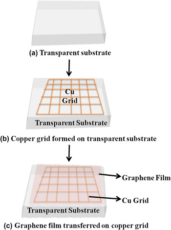
A schematic illustration of the processing steps for fabricating the hybrid transparent electrode is shown in Fig. 1. A transparent substrate (e.g., glass) was used as shown in Fig. 1(a). The desired thickness of copper was sputter deposited (Unaxis LLS EVO Sputtering System, Unaxis Balzers Limited, Balzers, Liechtenstein) onto the surface of the glass substrate. The copper grid was defined via photolithography and the copper film was etched with copper etchant (Transene Copper Etchant 49-1, Transene Company Inc., Danvers, MA) [Fig. 1(b)]. This was followed by the transfer of a monolayer of graphene film onto the copper grid [Fig. 1(c)].
Schematic illustration of processing steps for fabricating hybrid transparent electrodes. (a) A transparent substrate is used. (b) A copper film is sputtered onto the transparent substrate and the film is patterned via photolithography and etched to form the copper grid. (c) The graphene film is transferred onto the copper grid.

The transfer of the graphene film onto the copper grid was carried out as follow: the graphene film grown on a copper foil was attached to a piece of polydimethylsiloxane (PDMS) stamp and immersed in a copper etchant solution (Transene Copper Etchant 49-1). The copper foil was etched away, leaving behind the graphene film adhered to the PDMS stamp. The graphene film on PDMS stamp can be transferred onto the copper grid by conformally contacting the PDMS stamp to the copper grid and then peeling back the stamp on a hot plate.Reference Kim, Zhao, Jang, Lee, Kim, Kim, Ahn, Kim, Choi and Hong15
Electrical characterization of the hybrid transparent electrodes was performed in ambient air using Keithley 2612A SourceMeters (Keithley Instruments Inc., Cleveland, OH), and the transmittance spectra of the electrodes were measured using an ultraviolet (UV)–visible–near infrared (NIR) spectrometer (Shimadzu UV-3101PC, Shimadzu Corporation, Kyoto, Japan). Raman spectroscopy was performed using Renishaw inVia Raman Microscope (Renishaw, Hoffman Estates, IL).
III. RESULTS AND DISCUSSION
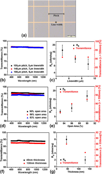
The electrical and optical properties of the hybrid transparent conductor can be controlled by designing the metal grid.Reference Kang and Guo27Figure 2(a) shows an optical image of a copper grid. The pitch and linewidth of the copper grid are defined as the distance between two grid lines and the width of the grid lines, respectively, as shown in Fig. 2(a). The pitch and linewidth can be easily varied by the design of the mask used for photolithography. The pitch and linewidth of the grid determine the clear aperture in the grid. The clear aperture is:  ${\rm{clear}}\,{\rm{aperture}}\,(\% ) = \left( {{{{\rm{pitch}} - {\rm{line}}{\rm{width}}} \over {{\rm{pitch}}}}} \right)^2 \times 100$. Another important variable is the thickness of the copper grid, which is determined by the thickness of the copper film deposited. We examine the relative importance of each design variable to determine the best approach to achieve a high electrical conductivity and high optical transmittance transparent conductor.
(a) Optical image of the copper square grid with a thickness of 45 nm, pitch of 100 μm, and linewidth of 5 μm. The scale bar is 50 μm. (b) Optical transmittance spectra of three copper square grids with 45 nm thickness and ∼90% open areas [100 μm pitch and 5 μm linewidth (black symbols), 140 μm pitch and 7 μm linewidth (red symbols), and 180 μm pitch and 9 μm linewidth (blue symbols)], measured with a UV–visible spectrometer, without including the substrates. (c) Sheet resistance (black square symbols) and transmittance measured at 550 nm (red circle symbols) as a function of the linewidth of the copper grids with ∼90% open areas and thickness of 45 nm. (d) Optical transmittance spectra of three copper square grids with 45 nm thickness and ∼90% (black symbols), ∼86% (red symbols), and ∼83% (blue symbols) open area, measured with a UV–visible spectrometer, without including the substrates. (e) Sheet resistance (black square symbols) and transmittance measured at 550 nm (red circle symbols) as a function of the percentage of open areas in the copper grids with thickness of 45 nm and pitch of 100 μm. (f) Optical transmittance spectra of the copper square grids with 100 μm pitch, 9 μm linewidth, and 45 nm (black symbols) and 130 nm (red symbols) thicknesses, measured with a UV–visible spectrometer, without including the substrates. (g) Sheet resistance (black square symbols) and transmittance measured at 550 nm (red circle symbols) as a function of the thickness of the copper grids with pitch of 100 μm and linewidth of 9 μm.

Figure 2(b) shows the transmittance spectra of three copper square grids with 45 nm thickness and ∼90% clear aperture, measured with a UV–visible spectrometer. Background subtraction using a blank substrate was performed to exclude the absorption of the substrate. The transmittance spectra of the copper grids are uniform in the visible to near-infrared range (i.e., 400–1200 nm). The grids are highly transparent, with the transmittance close to 90%. This is desirable for photovoltaic cell applications because a large portion of the solar spectrum falls in the visible and near-infrared range. Transmittance through a metal grid with a larger clear aperture is expected to be higher as less light is reflected or absorbed. Metal grids with similar clear aperture do not have vastly different transmittance spectra, as shown in Fig. 2(b). Figure 2(c) shows that a larger pitch and a larger linewidth but similar clear aperture results in similar transmittance at a wave length of 550 nm (∼90%) but somewhat lower sheet resistance. The sheet resistances of the copper grids with a 100-μm pitch and 5-μm linewidth, a 140-μm pitch and 7-μm linewidth, and a 180-μm pitch and 9-μm linewidth are 17 ± 3 Ω/□, 12 ± 2 Ω/□, and 9 ± 3 Ω/□, respectively. The slightly lower sheet resistance of the larger pitch and linewidth grid is likely due to reduced surface scattering as the linewidth of the grid lines increases.
Figure 2(d) shows the optical transmittance of three copper square grids with 45 nm thickness, 100 μm pitch, and 5 μm linewidth (black symbols), 7 μm linewidth (red symbols), and 9 μm linewidth (blue symbols). The grids with linewidths of 5, 7, and 9 μm have clear apertures of 90%, 86%, and 83%, respectively. As discussed earlier, transmittance through a metal grid with a larger clear aperture is higher, as shown in parts (d) and (e) of Fig. 2. The increase in transmittance is small (i.e., from 88% to 91% at the wave length of 550 nm) as the clear aperture increases from 83% to 90%. Anomalous transmission (i.e., transmission larger than the clear aperture) is observed because some light is transmitted through the nanoscale thick metal grid lines. Figure 2(e) also shows that a larger clear aperture results in a higher sheet resistance. The sheet resistances of the copper grids with 83%, 86%, and 90% clear aperture are 8 ± 1 Ω/□, 10 ± 2 Ω/□, and 17 ± 3 Ω/□, respectively. The increase in sheet resistance when the clear aperture is 90% is approximately twice that of the grid with 83% clear aperture. It is worth noting that the electrical conductivities of these copper grids are ∼2 × 10⁶ S/m, approximately 3.5% that of bulk copper metal film (∼5.8 × 10⁷S/m). This fraction of conductivity (∼3.5%) is close to the fractional area of the copper grid filled by the copper film [∼15% (100% − ∼85%)]. The slightly lower fraction of conductivity we observed in these copper grids (∼3.5% instead of ∼15%) is due to the reduced conductivity expected when the thickness of the copper grids is very small (45 nm).Reference Zhang, Brongersma, Richard, Brijs, Palmans, Froyen and Maex28
Next, we examine the effect of the thickness of the copper grid on the electrical and optical properties of the copper grid film. Figure 2(f) shows the optical transmittance of two copper square grids with 100 μm pitch and 9 μm linewidth and thicknesses of 45 and 130 nm. The 130-nm copper grid has a lower transmittance because less light can be transmitted through a thicker film of metal. The 130-nm copper grid also has a lower sheet resistance as shown in Fig. 2(g). The transmittance at 550 nm is decreased marginally from 88% to 85% when the thickness of the copper grid is increased from 45 to 130 nm. However, the decrease in sheet resistance is very significant (from 8 ± 1 Ω/□ to 2 ± 1 Ω/□) when the copper grid is thicker. This provides an attractive method to achieve copper grids with low sheet resistance without compromising the optical transmittance significantly. This method is more effective than increasing the linewidth of the copper grid. The sheet resistance decreases by 4 times compared to the 2 times achieved when a broader grid line is used. In both cases, the optical transmittance at a wave length of 550 nm decreases by 3%. The outcome of our study provides unprecedented guidelines for future design of metal grids used in high performance transparent conductors.
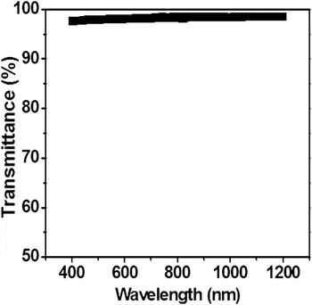
Besides the thin copper grid, the other component of the hybrid transparent conductor is the graphene film. The graphene film grown via chemical vapor deposition is found to have very high transmittance (98%) at a wave length of 550 nm, as shown in Fig. 3. Like the thin copper grid, the transmittance spectrum of the graphene film is very uniform in the visible and near-infrared range. The sheet resistance of the graphene film is 4 ± 3 kΩ/□, which is within the range found in literature.Reference Li, Zhu, Cai, Borysiak, Han, Chen, Piner, Colombo and Ruoff13, Reference Unarunotai, Koepke, Tsai, Du, Chialvo, Murata, Haasch, Petrov, Mason, Shim, Lyding and Rogers29 Evidently, the sheet resistance of the graphene film is approximately two orders of magnitude higher than that of the copper grid. The overall sheet resistance of the hybrid transparent conductor can be expressed as: 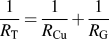 ${1 \over {R_{\rm{T}} }} = {1 \over {R_{{\rm{Cu}}} }} + {1 \over {R_{\rm{G}} }}$, where R T, R Cu, and R G are the sheet resistances of the hybrid transparent conductor, copper grid, and graphene film, respectively. When
 $R_{\rm{G}} \gg R_{{\rm{Cu}}} $,
 ${1 \over {R_{\rm{G}} }}$ is negligible and
 $R_{\rm{T}} \approx R_{{\rm{Cu}}} $. Hence, the sheet resistance of the hybrid transparent conductor is largely dominated by the thin copper grid. As the optical transmittance of the graphene film is higher than that of the thin copper grid, the optical transmittance of the hybrid transparent conductor is also largely limited by the thin copper grid. Nevertheless, the graphene film is essential for “filling up the voids” in the thin copper grid to form a continuously conducting film. A continuously conducting film is desired when applied in a solar cell because it decreases the series resistance in the cell, which increases the short-circuit current, resulting in a solar cell with higher efficiency.
Optical transmittance spectrum of a monolayer of graphene measured with a UV–visible spectrometer. Background subtraction using a blank substrate was performed to exclude the absorption of the substrate.

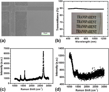
Hybrid transparent conductors that use thin metal grids and graphene films are discussed next. Figure 4(a) shows a scanning electron microscope (SEM) image of a monolayer of graphene transferred on a thin copper grid. A faint line in the middle of the figure shows the edge of the graphene. The graphene lies to the left of the faint line but not to the right. The Raman spectra of a monolayer of graphene transferred on a copper grid and the copper grid before a monolayer of graphene was transferred on it can be found in parts (c) and (d) of Fig. 4, respectively. The Raman spectrum in Fig. 4(c) shows distinctive Raman features of graphene (i.e., a small D peak at ∼1350 cm−1, a G peak at ∼1580 cm−1, and a 2D peak at ∼2700 cm−1, which is of higher intensity than that of the G peak),Reference Ferrari30, Reference Ferrari, Meyer, Scardaci, Casiraghi, Lazzeri, Mauri, Piscanec, Jiang, Novoselov, Roth and Geim31 which are absent in Figure 4(d), confirming the successful transfer of graphene onto the thin copper grid.
(a) SEM image of a monolayer of graphene transferred on a copper grid. A faint line in the middle of the figure shows the edge of the graphene. The graphene lies to the left of the faint line but not to the right. (b) Optical transmittance spectrum of a copper grid with a monolayer of graphene transferred on top of it measured with a UV–visible spectrometer, without including the substrate. Inset: digital camera image of the hybrid transparent conductor on a transparent substrate. The hybrid transparent conductor comprised of the copper square grids of various linewidths and pitches as mentioned in the text, and thicknesses of 45 nm with a monolayer of graphene transferred on top of it. A piece of paper with the words “TRANSPARENT” written on it, placed below the sample, is clearly visible. (c) Raman spectrum of a monolayer of graphene transferred on a copper grid. (d) Raman spectrum of the copper grid without a monolayer of graphene transferred on it.

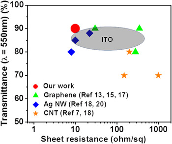
Figure 4(b) shows that the transmittance spectrum of the hybrid transparent conductor is approximately constant between the wave length of 400 and 1200 nm and high (∼90%). This is expected as both the transmittance spectra of the component materials, thin copper grid and graphene film, are very uniform between the wave length of 400 and 1200 nm and high. A digital camera image of the hybrid transparent conductor on a transparent substrate is shown in the inset. The hybrid transparent conductor is comprised of the copper square grids of various linewidths and pitches, and thicknesses of 45 nm with a monolayer of graphene transferred on top of it. A piece of paper with the words “TRANSPARENT” written on it, placed below the sample, is clearly visible. Evidently, the transparent conductor is hardly visible. The sheet resistance of a hybrid transparent conductor (graphene film transferred on a 7-μm linewidth and 100-μm pitch copper grid) is ∼10 Ω/□, which is similar to the sheet resistance of a copper grid of a similar design. As mentioned earlier in the text, the sheet resistance and optical transmittance are dominated by the copper grid. The transmittance at 550 nm and sheet resistance of the hybrid transparent conductor are comparable to the best transparent conductors reported so far, as shown in Fig. 5. Hence, the hybrid transparent conductor is a very promising approach to substitute ITO thin films.
Transmittance at 550 nm and sheet resistance of various transparent conductors studied in previous works and in this work. The hybrid transparent conductor we measured, graphene film, silver nanowire (Ag NW) film, and CNT film are represented by red circle, green triangle, blue diamond, and orange star symbols, respectively. ITO film is represented by the shaded gray area.

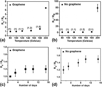
A transparent conductor that is thermally stable is desired for operation at elevated temperatures. The thermal stability of the hybrid transparent conductor (i.e., graphene film stacked on top of the copper grid) is investigated, as shown in Fig. 6(a). After being heated at 80, 100, 120, and 150 °C for an hour each in ambient air, the resistance of the hybrid transparent conductor hardly changes. This is not surprising after we find that the resistance of a copper grid only conductor (with similar grid design) remains approximately constant when subjected to similar thermal stresses, as shown in Fig. 6(b). But obvious degradation is observed after both the conductors are heated at 200 °C for an hour in ambient air. Investigation from another workReference Chen, Brown, Levendorf, Cai, Ju, Edgeworth, Li, Magnuson, Velamakanni, Piner, Kang, Park and Ruoff26 shows that various copper oxides [i.e., Cu2O, CuO, and Cu(OH)2] form when copper foil is heated to 200 °C, resulting in degradation of the copper metal. The earlier workReference Chen, Brown, Levendorf, Cai, Ju, Edgeworth, Li, Magnuson, Velamakanni, Piner, Kang, Park and Ruoff26 has also shown that graphene film grown on copper foil is able to protect the underlying copper foil from oxidation at 200 °C for 4 h in ambient air. In this work, we show that when the graphene film is transferred from the copper foil to another substrate (i.e., copper grid on glass substrate), the graphene film is still an effective barrier to retard the oxidation of the copper grid. Normalized resistances (R s/R 0) of the hybrid transparent conductor and the copper grid only conductor increase to ∼7 and ∼80, respectively. R 0 and R sare the sheet resistances before and after heat treatment, respectively. The normalized resistance of the copper grid only conductor is approximately an order of magnitude higher than the hybrid transparent conductor. This shows that the graphene film is effectively retarding the degradation of the copper grid. However, the hybrid transparent conductor also shows a small extent of degradation despite the presence of the graphene film. This can be due to the presence of defects/pinholes in the graphene film introduced during transfer, which provides a pathway for the ambient gases to permeate through. Transferring more layers of graphene films on top of the copper grid may be able to decrease the number of such pathways in the hybrid conductor and thus forms a better barrier.
(a–b) Variation of sheet resistance of a copper grid (a) with a monolayer of graphene film transferred on top of it and (b) without a monolayer of graphene film transferred on top of it after being heated at various temperatures: 80, 100, 120, 150, 180, and 200 °C for an hour each. R 0 and R s are the sheet resistances before and after heat treatment, respectively. The numbers in brackets above the symbols at temperatures between 80 and 180 °C represent the R s/R 0at those temperatures. (c–d) Variation of sheet resistance of a copper grid (c) with a monolayer of graphene film transferred on top of it and (d) without a monolayer of graphene film transferred on top of it after being heated at 100 °C for various amounts of time: 1 day, 3 days, 7 days, 10 days, and 15 days.

We also examine the stability of the transparent conductors with time. Parts (c) and (d) of Fig. 6 show the normalized resistances of the hybrid transparent conductor and the copper grid only conductor after being heated at 100 °C for varying amounts of time, respectively. After 15 days, the hybrid transparent conductor (R s/R 0 = 1.2 ± 0.1) displays slightly better thermal stability than the copper grid only conductor (R s/R 0 = 1.5 ± 0.1). The graphene film in the hybrid transparent conductor helps to retard the degradation of the copper grid, as explained earlier in the text. Nonetheless, both transparent conductors show fairly stable performance (R s/R 0< 2) after 15 days at 100 °C. This reflects that the hybrid transparent conductor can be thermally stable for an extended period of time and may be used for operation at temperatures up to 200 °C.
IV. CONCLUSIONS
We have examined the optical and electrical properties of the hybrid transparent conductor, which consists of a thin metal grid and graphene film. The overall performance is comparable to that of ITO thin films and is largely dominated by the geometry of the metal grid. We find that the most effective method to achieve high transmittance and low sheet resistance is to increase the thickness of the metal grid because an increase in thickness can result in a large decrease in sheet resistance but a small decrease in transmittance. We have also investigated the thermal stability of the hybrid transparent conductor because it may be integrated into devices that operate at high temperatures. The hybrid transparent conductor is thermally stable at 100 °C after 15 days, and the graphene film acts as an effective barrier to retard the oxidation of the copper grid at higher temperature in air. Hence, we have demonstrated a carefully designed hybrid transparent conductor that displays superior electrical, optical, and thermal stability properties.
ACKNOWLEDGMENT
This work was supported by the Agency of Science, Technology, and Research (A*STAR), Singapore.