I. INTRODUCTION
Semiconductor nanowires (NWs) have attracted a great deal of attention for use in future nanometer-scale electronic and optical devicesReference Hiruma, Yazawa, Katsuyama, Ogawa, Haraguchi, Koguchi and Kakibayashi1–Reference Johnson, Choi, Knutsen, Schaller, Yang and Saykally6 because they have small diameters and large surface areas that enable high-density integration of active devices on various platforms and the fabrication of various kinds of functional devices through the use of heterostructures. The surface area to grow radial heterostructures enables the formation of core-shell or core-multishell (CMS) NWs. Moreover, top surfaces with small diameters enable the formation of axial heterostructures regardless of lattice mismatches. The use of core-shell or axial NWs gives some functionality to NW-based applications.
The main approach to grow NW is based on vapor–liquid–solid (VLS) mechanism,Reference Wagner and Ellis7 which uses catalysts and the liquid phase underneath metal particles for crystallization. In 1964, Wagner and Ellis reported the mechanism responsible for forming Si whiskers.Reference Wagner and Ellis7 VLS-grown III-V compound semiconductor nanowhiskers were investigated in the early 1990s.Reference Hiruma, Katsuyama, Ogawa, Koguchi, Kakibayashi and Morgan8 The potential of NWs to be applied to future electronics and photonics was demonstrated in the early 2000s after this pioneering work.Reference Huang, Duan, Cui, Lauhon, Kim and Lieber2–Reference Johnson, Choi, Knutsen, Schaller, Yang and Saykally6, Reference Björk, Ohlsson, Sass, Persson, Thelander, Magnusson, Deppert, Wallengerg and Samuelson9 Since then, VLS has become exceedingly common because this method can be used to synthesize almost all semiconductor NWs through rather simple procedures. The metal catalysts, however, often act as unintended impurities inside the NWs and form deep levels that could degrade the optical and electrical properties.Reference Yan and Milnes10 The self-catalyzed method has recently been investigated to grow NW regardless of the unintended impurities resulting from metal catalysts.Reference Morral, Colombo, Abstreiter, Arbiol and Morante11, Reference Mandl, Stangl, Hilner, Zakharov, Hilletich, Dey, Samuelson, Bauer, Deppert and Mikkelsen12
Another approach to grow NWs is catalyst-free selective-area growth (SAG). Selective-area metal-organic vapor-phase epitaxy (SA-MOVPE) is a kind of template method, which involves a combination of bottom-up (epitaxial growth) and top-down (lithography) approaches. This enables the fabrication of nanostructures with lithographically defined positioning. The masks used with this method are usually amorphous film, such as SiO2 and SiNx. The SAG technique was developed in the early 1960s and was first used for Si-integrated circuits.Reference Joyce and Baldrey13 In 1965, Tausch and Lapierre were the first to investigate the SAG of GaAs,Reference Tausch and Lapierre14 and Rai-Choudhury investigated the SAG of GaAs by using a metal-organic source.Reference Rai-Choudhury15 Then, Jones and Lau reported on the SAG of GaAs by using a lithography-defined native oxide patterns.Reference Jones and Lau16 The use of (111) B-oriented substrates enabled the formation of inclined {110} facets and vertical {1−10} facets. The formation of {1−10} vertical facets on a (111)B-oriented surface has been demonstrated by Fukui and Ando.Reference Fukui and Ando17 Tetrahedral GaAs have been fabricated by using this facet growth.Reference Fukui, Ando, Tokura and Toriyama18 Moreover, quantum dotsReference Kumakura, Nakakoshi, Motohisa, Fukui and Hasegawa19–Reference Miyoshi, Nakajima, Motohisa and Fukui21 have been selectively grown by using the selectively grown GaAs nanostructures. Vertical hexagonal nanostructures could be formed by using selectivity to form {1−10} facets and these structures have been applied to laser and photonic crystals.Reference Ando, Kobayashi and Ando22, Reference Hamano, Hirayama and Aoyagi23 Now, this approach is being used to grow NWs.
This approach uses partially masked templates with lithographically defined opening patterns. Position-controlled polygonal nanostructures surrounded by several facets can be formed inside the openings because crystal continues to grow through the mechanism of faceting growth. Because the direction of preferential growth for the III-V NWs is <111>A or <111>B directions, the use of III-V (111)A or B substrates enables formation of vertically aligned hexagonal pillars surrounded by {−110} vertical sidewalls. These position-controlled NWs have been achieved in III-V compound semiconductors, such as GaAs,Reference Motohisa, Noborisaka, Takeda, Inari and Fukui24–Reference Ikejiri, Sato, Yoshida, Hiruma, Motohisa, Hara and Fukui27 InP,Reference Mohan, Motohisa and Fukui28, Reference Kitauchi, Kobayashi, Tomioka, Hara, Hiruma, Fukui and Motohisa29 InAs,Reference Tomioka, Mohan, Noborisaka, Hara, Motohisa and Fukui30, Reference Akabori, Sladek, Hardtdegen, Schäoers and Grützmacher31 InGaAs,Reference Akabori, Takeda, Motohisa and Fukui32–Reference Yoshimura, Tomioka, Hiruma, Hara, Motohisa and Fukui35 and GaAsP,Reference Fujisawa, Sato, Hara, Motohisa, Hiruma and Fukui36 as well as nitridesReference Sekiguchi, Kishino and Kikuchi37 and oxides.Reference Kim, Lee, Hong, Yi, Kim and Cheong38 Position-controlled AlGaAs/GaAs,Reference Noborisaka, Motohisa, Hara and Fukui39 InAs/InP,Reference Mohan, Motohisa and Fukui40 and GaAsP/GaAsReference Hua, Motohisa, Kobayashi, Hara and Fukui41 core-shell NWs and InP/InAs/InPReference Mohan, Motohisa and Fukui42 CMS NWs have been reported by using SA-MOVPE. The position-controlled growth of InGaAs/GaAs,Reference Yang, Motohisa, Takeda, Tomioka and Fukui43, Reference Shapiro, Lin, Wong, Scofield, Tu, Senanayake, Mariani, Liang and Huffaker44 InAsP/InP,Reference Sasakura, Humano, Suemune, Motohisa, Kobayashi, van Kouwen, Tomioka, Fukui, Akopian and Zwiller45 and AlGaAs/GaAsReference Hayashida, Sato, Hara, Motohisa, Hiruma and Fukui46 axial heterostructured NWs has also been investigated.
This article reports on the position-controlled growth of III-V NWs by using SA-MOVPE, growth behavior in III-V (GaAs, InAs, and InP) NWs, and the demonstration of III-V NW-base devices such as light-emitting diodes (LEDs), solar cells, and vertical surrounding-gate transistors (VSGTs).
II. EXPERIMENTS
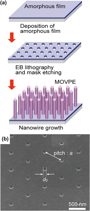
The growth process for SA-MOVPE is outlined in Fig. 1. After the substrate [Fig. 1(a)] is degreased, SiO2 films with a thickness of 10–30 nm are formed by RF sputtering, plasma-enhanced chemical vapor deposition, or thermal oxidation. Thermal oxidation is usually used to form SiO2 where III-V NW is grown on Si because of the thermal tolerance of the film. Next, circular openings with a regular pitch are formed on the amorphous films by using electron-beam lithography and wet-chemical etching. The etchant solution was buffered hydrogen fluoride. The circular openings are arranged in a triangular lattice with a pitch of 0.4–3.0 μm. The opening diameter, d 0, ranges from 20–400 nm. The d 0 was around 70–300 nm for the use of the NWs in optical applications. Reactive-ion etching (RIE) with CF4 gas is sometimes used for etching. It should be noted that surface damage because of etching should be considered in this case because the surface damage degrade the SA-MOVPE. In most cases, we use the wet etching to avoid such surface damage. Scanning electron microscopic (SEM) image of the masked substrate is shown in Fig. 1(b). Finally, the NWs are grown by MOVPE. The (111)B- or (111)A-oriented surfaces are used for NWs grown by SA-MOVPE because the III-V NWs are preferentially grown in <111>A or <111>B directions. The (111)A surface has its topmost layer arranged with group-III atoms, and the (111)B surface has its layer arranged with group-V atoms.
(a) Fabrication process for selective-area metal-organic vapor-phase epitaxy (SA-MOVPE). After amorphous film is deposited, hole openings are formed by lithography and etching. Nanowires (NWs) are grown by MOVPE. (b) Scanning electron microscopic (SEM) image of patterned substrate.
The NWs were grown using a low-pressure (0.1 atm) horizontal-reactor MOVPE system. The carrier gas used in this growth was pure hydrogen (H2) that had been purified by passing it through a Pd film. The total flow rate of the gases was maintained at 5.75 standard liters per minute. The group-III-atom precursors used in this study were trimethylgallium (TMGa), trimethylindium (TMIn), and trimetylaluminium (TMAl), and the group-V-atom precursor was 5% arsine (AsH3) in H2 and tertiary butyl phosphine (TBP). Monosilane (SiH4) gas was used for n-type doping and diethylzinc was used for p-type doping.
Micro-photoluminescence was carried out at 4 K. The excitation light was an He-Ne laser, which was focused on an ∼2-μm spot on the substrate. Approximately 10 NWs were included in the spot.
III. SA-MOVPE GROWTH OF III-V NWS
A. Dependence of GaAs growth on substrate orientations in SA-MOVPE
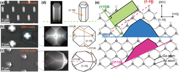
Figure 2 shows the dependence of the growth on substrate orientations in the SA-MOVPE of GaAs. For NWs grown by VLS,Reference Wagner and Ellis7 self-catalyzed VLSReference Hiruma, Katsuyama, Ogawa, Koguchi, Kakibayashi and Morgan8, and oxide-assisted growth,Reference Shi, Zheng, Wang, Lee and Lee47 the III-V NWs preferentially grew in the <111>B directions. This direction of preferential growth of NWs is independent of the surface orientations. Therefore, vertical III-V NWs are formed on the (111) B-oriented surface and tilted III-V NWs are formed on (001) and (110) substrates.Reference Hiruma, Yazawa, Katsuyama, Ogawa, Haraguchi, Koguchi and Kakibayashi1 However, NWs grown with SA-MOVPE are dependent on substrate orientation because of faceting growth.
SA-MOVPE of GaAs on (a) GaAs (111)B substrate, (b) GaAs (001) substrate, and (c) GaAs (311)B substrate. Images summarize structures grown under high T G and low [AsH3]. (d) SEM images and schematics of crystal shapes on GaAs (111)B, (001), and (311)B. Schematic of GaAs crystal structure with injection of [1-10] direction. (e) Illustrations show cross-sections of structures in (d). Dashed line indicates family of {1-10} planes. These planes are normal to (111)A or (111)B surface.

Equilibrium crystal shapes have a polygonal morphology surrounded by close-packed planes with a minimum surface energy.Reference Dobrusin, Kotechy and Shlosman48 The low surface energy results in a stable surface with a slow growth rate. Thus, a crystal shape surrounded by stable crystal planes is formed by the faceting growth. This property clearly appears in SAG as can be seen in Figs. 2(a)–2(c). The crystal shapes grown with SAG structure have some low index planes. The origin of faceting in SAG can simply be explained by the difference in the surface chemical potential of the planes, i.e., the number of dangling bonds. This is because the growth rate roughly depends on the number of dangling bonds of the surface. The atomic arrangement of GaAs from the <1−10> direction is shown in Fig. 2(e). Some low index planes are arranged on the (001) planes. Interestingly, one of the family of {110} planes, the {1−10} plane (red dashed line) is arranged normal to the (111)A or (111)B planes in this diagram. The planes are formed as facets during SA-MOVPE.
The growth rate of the GaAs (001) surface is independent of the variations in the growth temperature (T G) and the partial pressure of AsH3 ([AsH3]) because of diffusion-limited growth. However, the growth rate of the GaAs (110), (111)A, and (111)B surfaces varies with T G and [AsH3]. The growth rate of the GaAs (111)B surface becomes faster than that of GaAs (011) and (111)A surfaces under high T G and low [AsH3]. This is because the group-III adatoms easily evaporate from the {1−10} surfaces under high T G. Polygonal nanostructures surrounded by {1−10}, (111)B, and (111)A planes are formed on GaAs (001) and (311)B substrates in this way, as shown in Figs. 2(b)–2(d). Also, tetrahedral structures surrounded by (111)A surfaces are formed under high T G and low [AsH3] (not shown here). Interestingly, the crystal shape of GaAs on (111)B-oriented surfaces becomes hexagonal pillars surrounded by vertical {1−10} facets. This is because the family of {−110} planes are vertically arranged from the (111)B surface. Therefore, hexagonal III-V NWs surrounded by {1−10} vertical facets can be formed on the (111)B-oriented surface because these tendencies in the SAG of GaAs are commonly observed in other III-V compound semiconductors except for InP. It should be noted that vertical InP NWs are formed on (111)A-oriented surfaces in SA-MOVPE.Reference Ikejiri, Sato, Yoshida, Hiruma, Motohisa, Hara and Fukui27 This is because direction of the preferential growth for InP NWs is in the <111>A direction and phosphorous trimers can be formed on the InP (111)A surface.Reference Li, Sun, Law, Visbeck and Hicks49 The growth rate of GaAs (111)A and (110) surfaces, on the other hand, becomes faster than that of (111)B planes under low T G and high [AsH3]. This is because the As-trimers formed on the (111)B surface suppress nucleation on the GaAs (111)B surface.Reference Biegelsen, Bringans, Northrup and Swartz50 Controlling of the growth condition enables the formation of core-shell NWs.
B. Growth of III-V NWs by SA-MOVPE
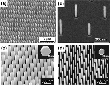
Figure 3 depicts the typical results for III-V NWs grown with SA-MOVPE. Figure 3(a) shows the GaAs NWs grown on a GaAs(111)B substrate. The diameter of the NWa is 70 nm and height is 3 μm. Figure 3(b) shows InAs NWs grown on an InP(111)B substrate with a diameter of 20 nm and a height of 400 nm. Figures 3(c) and 3(d) show InP NWs grown on InP(111)A under different growth conditions.Reference Ikejiri, Sato, Yoshida, Hiruma, Motohisa, Hara and Fukui27 The diameter of NWs shown in Fig. 3 were equal to the opening diameter. In case of Fig. 3(b), the edge of the openings was tapered due to isotropic etching of HF solution. The diameter of the InAs NWs shown in Fig. 3(b) corresponded to that of the bottom window of opening. Position-controlled III-V NWs were successfully grown on III-V(111)B or (111)A substrates. Nanometer-scale growth with SA-MOVPE has recently enabled the formation of III-V NWs on lattice mismatched substrates regardless of lattice mismatching.Reference Tomioka, Motohisa, Hara and Fukui51–Reference Hertenberger, Rudolph, Bichler, Findley, Abstreiter and Koblmüller54 The optimum conditions for III-V NWs by the SA-MOVPE will not change under these heteroepitaxial systems. We will next briefly summarize the optimum conditions and typical behaviors to grow these III-V NWs in SA-MOVPE.
Typical results for III-V NWs grown by SA-MOVPE. (a) GaAs NWs with diameter of 70 nm and height of 3 μm. Substrate is GaAs(111)B. (b) InAs NWs with diameter of 20 nm and height of 400 nm. Substrate is InP(111)B. (c) InP NWs grown at 600 °C and V/III ratio 55. (d) InP NWs grown at 660 °C and V/III ratio of 18.
1. GaAs NW
The optimum T G window ranged from 700 to 750 °C.Reference Motohisa, Noborisaka, Takeda, Inari and Fukui24–Reference Ikejiri, Sato, Yoshida, Hiruma, Motohisa, Hara and Fukui27 The metal-organic (MO) sources were TMGa and AsH3. Tertiarybutyl arsine is sometimes used to grow the NWs.Reference Sladek, Klinger, Wensorra, Akabori, Hardtdegen and Grützmacher55 The GaAs NWs were formed under a V/III ratio of 100–250. The optimum T G window for GaAs NWs was the boundary between the formation of As-trimers and the desorption of adatoms on the (111)B surface. The As-trimer forming on the (111)B surface became dominant below the optimum T G, and their formation suppressed GaAs growth on the (111)B surface. Here, lateral over-growth (LOG) along the <1−10> direction is dominant because the growth rate of {1−10} sidewalls is faster than that of the (111)B surface. However, the desorption of adatoms is enhanced above the optimum T G because desorption-limited growth occurs in these temperature ranges. The LOG is almost suppressed above the optimum T G, where the growth rate of GaAs NWs is decreased because of desorption. Also, the growth rate of {1−10} sidewalls is suppressed because of the desorption of group-V atoms. The use of optimum growth conditions for GaAs enabled the growth of highly uniform NW arrays as shown in Fig. 3(a). GaAs NWs can be grown on Si(111) substrates.Reference Tomioka, Kobayashi, Motohisa, Hara and Fukui52
The height of GaAs NWs is inversely proportional to the opening diameter of the mask in Fig. 4(a).Reference Ikejiri, Sato, Yoshida, Hiruma, Motohisa, Hara and Fukui27 This suggests that the migration of growth species on the NW sidewalls plays a major role in the SAG of GaAs NWs.
Dependencies of NW height on diameter: (a) GaAs NWs, (b) InAs NWs, and (c) InGaAs NWs.

2. InAs NW
Figure 3(b) shows the InAs NWs grown on an InP(111)B substrate (lattice mismatch is 3.3%). Very thin InAs NWs with a diameter of 20 nm were grown on an InP(111)B substrate that was patterned with lithography. The optimum T G window ranged from 540 to 580 °C.Reference Tomioka, Mohan, Noborisaka, Hara, Motohisa and Fukui30 This optimum T G window is typical for the H2 carrier gas. In case of nitrogen carrier gas, the T G window changes from 650 to 700 °C.Reference Akabori, Sladek, Hardtdegen, Schäoers and Grützmacher31 The MO sources were TMIn and AsH3. The InAs NWs were formed under a V/III ratio of 250 with SAG. The LOG was enhanced below the optimum T G, and the growth rate for InAs NW was reduced above the optimum T G.Reference Tomioka, Mohan, Noborisaka, Hara, Motohisa and Fukui30 The mechanism for these behaviors was the same as the GaAs NWs with SAG. The height of the InAs NWs was inversely proportional to the square of the opening diameter of the mask shown in Fig. 4(b).Reference Tomioka, Mohan, Noborisaka, Hara, Motohisa and Fukui30 This means that the surface diffusion of growth species on the SiO2 and NW sidewalls played a major role in NW growth. We confirmed that InAs NWs could be grown on (111)B-oriented substrates and a Si(111) substrate.Reference Tomioka, Motohisa, Hara and Fukui51, Reference Hertenberger, Rudolph, Bichler, Findley, Abstreiter and Koblmüller54
3. InP NW
The optimum T G window ranged from 600 to 660 °C.Reference Mohan, Motohisa and Fukui28 The MO sources were TMIn and TBP. The InP NWs were formed under a V/III ratio of 15–60 with SAG. The direction of preferential growth was <111>A. Thus, vertical InP could be formed on the (111)A substrate. The LOG was enhanced below the optimum T G and high [TBP]. The distinct feature of InP NWs is their different morphology and crystal structure. The morphology of the InP NWs achieved a straight and cylindrical structure under low T G and a high V/III ratio, as shown in Fig. 3(c), and a tapered structure was formed under high T G and a low V/III ratio, as shown in Fig. 3(d). Recently, we found that these different-shaped InP NWs had different crystal structures. The tapered InP NWs exhibited wurtzite structure with few stacking faults, and the straight InP NWs exhibited a twin-included zincblende structure.Reference Kitauchi, Kobayashi, Tomioka, Hara, Hiruma, Fukui and Motohisa29
4. InGaAs NW
The optimum T G to form InGaAs NWs on InP(111)B ranged from 630 to 670 °C,Reference Akabori, Takeda, Motohisa and Fukui32–Reference Sato, Kobayashi, Motohisa, Hara and Fukui34 and the T G to form InGaAs NWs on GaAs(111)B ranged from 650 to 700 °C.Reference Yoshimura, Tomioka, Hiruma, Hara, Motohisa and Fukui35 Moreover, the In/Ga composition varied with the NW pitch due to the migration of growth species on SiO2 and NW sidewalls. For instance, the Ga composition of InGaAs NWs changed from 62 to 80% with decreasing pitch from 6 to 0.6 μm.Reference Sato, Kobayashi, Motohisa, Hara and Fukui34 The MO sources were TMIn, TMGa, and AsH3. The height of InGaAs NWs was inversely proportional to the square of the opening diameter of the mask shown in Fig. 4(c).Reference Sato, Kobayashi, Motohisa, Hara and Fukui34 This was because the surface migration of In atoms was dominant during InGaAs NW growth.
5. GaP NW
Figure 5 shows SAG of GaP grown on GaP(111)A and (111)B substrates. Pyramidal structures surrounded by {111}B surfaces were formed on GaP(111)A. Hexagonal GaP NWs, on the other hand, were formed on the GaP(111)B surface. The direction of preferential growth was <111>B. The optimum T G window ranged from 770 to 790 °C, as shown in Fig. 6. The MO sources were TMGa and TBP. The GaP NWs were formed under a V/III ratio of 200–250 with SAG.
Plan view of GaP growth on (a) GaP(111)A and (b) GaP(111)B surfaces.

SEM images for dependence of GaP NW growth on T G: (a) T G = 750 °C, (b) T G = 770 °C, (c) T G = 790 °C, and (d) T G = 820 °C.

C. Growth of core-shell NWs by SA-MOVPE
The most distinctive feature of SA-MOVPE for NW growth is the isolation of the LOG and NW growth modes by T G or the V/III ratio. For example, low T G enhances the LOG of GaAs without any NW growth after GaAs NWs were grown under optimum T G.Reference Ikejiri, Sato, Yoshida, Hiruma, Motohisa, Hara and Fukui27 The diameter of the GaAs NWs becomes larger than that of the mask opening without NW growth. This is because the growth rate of the {1−10} sidewall increased due to the suppressed desorption process on the {1−10} sidewalls. This tendency was similarly observed in other materials. The use of this property to grow heterostructures enabled us to form core-shell or CMS NWs such as GaAs/AlGaAs core-shell NWs.Reference Noborisaka, Motohisa, Hara and Fukui39 Figure 7(a) shows results of the GaAs/AlGaAs core-shell NWs grown on Si substrate.Reference Tomioka, Kobayashi, Motohisa, Hara and Fukui52 LOG of the AlGaAs shell layer occurred only on the sidewalls of the GaAs NWs because the height of the NWs was the same before and after the AlGaAs shell layer were grown.
(a) Illustration of growth of GaAs/AlGaAs core-shell NWs and SEM image of GaAs NWs and GaAs/AlGaAs CS NWs on Si substrates. (b) Photoluminescence spectra of GaAs NWs and GaAs/AlGaAs CS NWs at 4 K.

The number of surface states of NWs could be increased more than that of planar III-V because the NWs have large surface areas on the NW sidewalls. These surface states degrade the optical properties of III-V NWs and device performance through a nonradiative recombination process. The core-shell structures effectively passivate these surface states of NWs. Also, the shell layer is more stable in the atmosphere as compared to sulfur passivation.Reference Skromme, Sandroff, Yablonovitch and Gmitter56 GaAs/AlGaAs core-shell NWs improved photoluminescence (PL) intensity up to 490-fold because of the reduction in the surface states shown in Fig. 7(b).Reference Tomioka, Kobayashi, Motohisa, Hara and Fukui52
IV. APPLICATIONS OF III-V NWS
There are two approaches to apply III-V NWs to devices owing to the structures. The first is to use epitaxial heterostructures for state-of-the art devices such as single photon emitters.Reference Borgström, Zwiller, Muller and Imamoglu57 The second is to fabricate core-shell structures for light sources and detectors. The use of core-shell structures would be essential for III-V NW-based applications in terms of surface passivation. Applications based on the latter approach have recently become exceedingly common because research on optical applications and photovoltaic devices using the geometric characteristics of NWs has been increasing. We have also reported the fabrication of GaAs/AlGaAs CMS NW-based near infrared (NIR)-LEDsReference Dorenbos, Sasakura, van Kouwen, Akopian, Adachi, Namekata, Jo, Motohisa, Kobayashi, Tomioka, Fukui, Inoue, Kumano, Natarajan, Hadfield, Zijlstra, Klapwijk and Suemune58 and InP core-shell NW-based solar cellsReference Goto, Nosaki, Tomioka, Hara, Hiruma, Motohisa and Fukui59 using radial p-n junctions.
A. Applications of III-V NWs to light sources
The light sources of semiconductor NWs were pioneered by Hiruma et al.Reference Hiruma, Yazawa, Katsuyama, Ogawa, Haraguchi, Koguchi and Kakibayashi1 They fabricated NIR-LEDs by using VLS-grown GaAs NWs with axial p-n junctions. After they reported this device, blue LED using GaN nanocolumns were demonstrated by Kishino et al. in 1996.Reference Kikuchi, Kawai, Tada and Kishino60 After that, optically pumped stimulated emissions from single GaN NW,Reference Johnson, Choi, Knutsen, Schaller, Yang and Saykally6 and multi-colored LEDs using GaN/InGaN CMS NWs were reported in early 2000s.Reference Qian, Gradečak, Li, Wen and Lieber61 The core-shell structure has one shell layer against the core NW, and the CMS structure has multilayer film on the sidewalls. The fabrications of CMS NW-based LEDs have recently been investigated for NIRReference Tomioka, Motohisa, Hara, Hiruma and Fukui62–Reference Chuang, Sedgwick, Chen, Ko, Moewe, Ng, Tran and C-Hasnain64 and blueReference An, Chae, Yi and Park65–Reference Lin, Lu, Chen, Lee and Gwo68 regions.
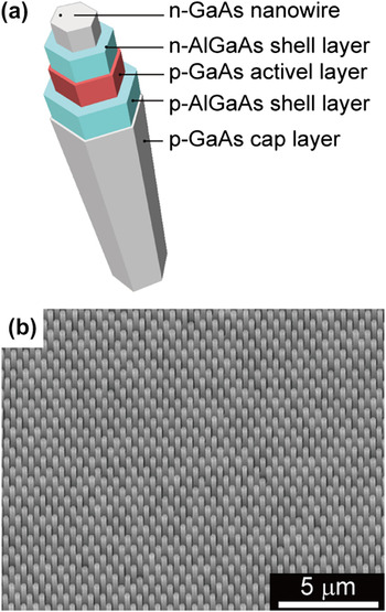
We designed the double-heterostructured (DH) CMS NWs shown in Fig. 8(a). These structures were to enhance emission efficiencies in NW-based LEDs. Their structure consists of an n-type GaAs NW as a core and n-AlGaAs, p-GaAs, p-AlGaAs, and p-GaAs shells for the innermost to outermost shells, which are sequentially grown on the sidewall of the GaAs core NW. The n-type and p-type AlGaAs layers are cladding layers to confine of electrons and holes in the inner p-GaAs layer for photon generation in the p-GaAs layers. The p-GaAs wedged between the n-AlGaAs and AlGaAs layers is a quantum well tube, while the outer p-GaAs is a capping layer for Ohmic contacts.
(a) Illustration of GaAs/AlGaAs core-multishell (CMS) NW. (b) SEM image of CMS NWs grown on GaAs(111)B substrate.

After the GaAs NWs had been grown, each n- and p-AlGaAs shell layer was formed at 700 °C for 5 min. Also, each p-GaAs well layer and capping layer was grown at 700 °C for 3 min. The nominal carrier concentrations of planar GaAs and p-GaAs were 3.5 × 1017 cm−3 and 4.0 × 1018 cm−3. The donor and acceptor concentrations, N D and N A, of planar n-AlGaAs and p-AlGaAs were 9.0 × 10¹⁷ and 1.0 × 1018 cm−3. The actual doping level in each layer of the CMS NWs was unknown because of the difficulty of characterizing such thin layers. As mentioned in a previous report regarding core-shell InP NW solar cells,Reference Kikuchi, Kawai, Tada and Kishino60 there is a possibility that these carrier concentrations for the CMS NWs were lower than those for the planar epitaxial layers.
Figure 8(b) shows the SEM image of the DH-CMS NW array on the n+-GaAs(111)B substrate. Vertically aligned regular hexagonal NWs with a diameter of 250 nm were fabricated on the substrate. The average height of the CMS NWs was 2 μm. Unintentional kink and taper formations in the NWs that resulted from high doping cannot be observed in these images. Thus, each NW had a uniform shell-layer thickness.
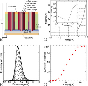
Figure 9(a) outlines the structure of NW-based LEDs. The details on the device process are explained in Ref. Reference Goto, Nosaki, Tomioka, Hara, Hiruma, Motohisa and Fukui59. The Cr/Au thicknesses were Cr(10 nm)/Au(130 nm) with 25-nm-thick n- and p-AlGaAs shell layers. About 105 NWs were connected in parallel in this LED structure. The total junction area was estimated to be 1.3 × 10⁻³ cm2. To determine what recombination mechanism was in the CMS NW–based LEDs on GaAs, we measured the current of CMS NW devices at voltages from −2 to 2 V using an HP 4156B parameter analyzer. The Cr/Au metals in these measurements were positively biased, and the Ge/Au/Ni/Au backside electrode was grounded. Figure 9(b) plots the current–voltage (I–V) curves for these structures. The I–V curves for all devices reveal moderate rectifying properties. The inset in Fig. 9(b) is a semi-logarithm plot of the I–V properties. The depletion width in this structure was estimated to be 23 nm and the total thickness of this CMS layer was more than the depletion width.
(a) Schematic of GaAs/AlGaAs CMS NW-based LEDs on GaAs. About 105 NWs are connected in parallel. (b) Current–voltage (I–V) curve for NW-based LEDs. (c) Electroluminescence (EL) spectra under several current injections at RT. (d) EL intensity as a function of injected current.

The rectifying properties for the CMS NW–based LED array with thick AlGaAs layers indicate gradual sub-linear curves resulting from unexpected resistance. The resistances originated from series and contact resistance across the NWs and Si substrate. Also, premature turn-on behaviorReference Schubert69 originating from surface states occurred. Considering the resistance (R S) with the CMS NW–based LEDs and shunt resistance to be infinity, the current equation is expressed as J(n) = J 0 exp[(V − R SI)/nkT], where n is the ideality factor of the p-n junction. From this equation, the n is estimated to be 1.03 for the device, and the R S is calculated to be 6.21 kΩ. The n for the device corresponds to that of conventional GaAs-based diodes (n ∼ 1.1–1.5). Such a good ideality factor means the high quality p-n junction was formed inside the CMS. The high R s is thought to result from contact resistance between the top Cr/Au and p-GaAs.
Figure 9(c) shows the typical electroluminescence (EL) spectra obtained under several current conditions. The threshold current for EL is 25 μA (current density is 15 mA/cm2) at 1.9 V. The EL peak position is around 1.42 eV. The EL peak position shifted to 60 meV from that of the GaAs bandgap at room temperature (RT, E g = 1.42 eV). This EL resulted from the GaAs active layer inside the DH. The full width at half maximum (FWHM) of EL was 120 meV, which was larger than the theoretical linewidth (1.8 kT) in LED spectra and the PL spectra at RT also showed large FWHM (not shown here). This is because the EL spectra shown in Fig. 9(c) contain several luminescence centers resulting from donor–acceptor pair transitions from Si, C, and Zn impurities in the AlGaAs layers.Reference Goto, Nosaki, Tomioka, Hara, Hiruma, Motohisa and Fukui59
The EL intensity increased super-linearly with current injection, and it was saturated from I = 90 μA (54 mA/cm2), as shown in Fig. 9(d). The super-linear characteristics in EL intensity at low current injection indicates that the CMS NW–based LED is similar to super-luminescence LED.Reference Ray, Groom, Liu, Hopkinson and Hogg70 This is because the AlGaAs shell layer surrounded by Cr/Au metal and oxides acts as a cavity because the reflectivity of the metal is above 95%. The origin of saturation was the carrier overflow effect as observed in surface-emitting LEDs. This is because the volume of the active region in the CMS NWs is very thin and parasitic resistance (e.g., contact and series resistance) is high. We concluded that CMS NW–based LEDs are super-luminescence surface-emitting LEDs. Moreover, no shift in the EL peak position resulting from the effect of Joule heating on the junction temperature was observed when the current injections were further increased. We have recently integrated these GaAs/AlGaAs CMS NWs with Si substrates.Reference Goto, Nosaki, Tomioka, Hara, Hiruma, Motohisa and Fukui59 The CMS NW–based LEDs integrated on Si also indicated similar properties as mentioned here.
B. Photovoltaic application of III-V NWsReference Kikuchi, Kawai, Tada and Kishino60
The periodical NW array structure has potential in photovoltaic applications to improve optical absorptionReference Hu and Chen71 while reducing optical reflections, and core-shell structures with radial p-n junctions,Reference Kayes, Atwater and Lewis72, Reference Kandala, Betti and Morral73 which are aligned parallel to incident light, are predicted to improve the collection efficiency of photo-generated electrons and holes across the junction area. The core-shell III-V NWs grown by SA-MOVPE provide both geometrical and electrical advantages for photovoltaic applications. Moreover, the NW array structure has the advantage of saving natural resources over conventional thin film photovoltaic devices. These advantages can be demonstrated by utilizing a well aligned array made of high quality NWs. Several photovoltaic applications of NWs have been reported,Reference Tian, Zheng, Kempa, Fang, Yu, Yu, Huang and Lieber74–Reference Mariani, Laghumavarapu, de Villers, Shapiro, Senanayake, Lin, Schwartz and Huffaker79 but periodically aligned NWs with uniform core-shell structures have less fabricated thus far. We have recently fabricated highly uniform InP core-shell NWs with radial p-n junctions and demonstrated InP NW–based photovoltaic device.Reference Kikuchi, Kawai, Tada and Kishino60 Here, we briefly review these progresses.
The growth conditions for core p-type InP NWs were described in Section III. B. 2. The sequences of crystal growth for intrinsic and n-type InP shell layers were carried out continuously by changing the growth conditions. The T G was decreased to 600 °C to grow the shell layer, and the partial pressure of TBP was increased to 1.1 × 10⁻⁴ atm to enhance lateral growth. The molar flow ratio of SiH4/TMI was 1.5 × 10⁻³ during the growth of n-type shell layer. Although the dopant concentration was not investigated in any layer of core-shell NWs, secondary-ion mass spectrometry analysis of the thin film crystal grown outside the NW array revealed that the concentration of Zn in the p-type layer was 6 × 10¹⁸ and that of Si in the n-type layers was 1 × 10¹⁸ atoms/cm3. Also a Zn concentration of up to 2 × 10¹⁸ atoms/cm3 was detected in the intrinsic layer between p-n junction. This was probably because of the memory effect of the Zn dopant inside the growth chamber or the Zn diffusion from the p-type core region.
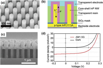
Figure 10(a) shows the growth result of InP core-shell NW array. The average diameter of core InP NWs was 135 nm and this was almost equal to that of the hole in the SiO2 mask pattern. This means that core NWs mainly grew perpendicular to the substrate, i.e., in the <111>A direction, with little lateral growth. After the shell layer had been grown, the diameter increased and became 209 nm on average. This increased diameter suggests the formation of a radial p-n junction as a core-shell structure. The NW array grown by SA-MOVPE was rather dense compared with the VLS NW array, and the filling factor was 27% [Fig. 10(a)]. Such a dense NW array was produced as a result of controlling the position and direction of all NWs grown by SA-MOVPE.
(a) SEM image of InP core-shell NW array. (b) Schematic cross-section of photovoltaic devices using core-shell InP NWs with radial p-n junctions. (c) cross-sectional SEM image of device. (d) Measured current–voltage curves of photovoltaic cell fabricated with core-shell InP NWs with radial p-n junctions.

We fabricated a photovoltaic device using a core-shell p-n junction InP NW array covering an area of 7.0 mm × 2.6 mm on a p-type InP(111)A substrate. The fabrication processes were the same as those to fabricate NW-LEDs. We used an indium-tin-oxide (ITO) film as a transparent electrode for the photovoltaic devices. The ITO film was sputtered on the NW array at RT, followed by heat treatment at 400 °C to reduce the resistance of ITO. Then, a comb-shaped Ag electrode as a carrier collector was also formed on the transparent ITO electrode. An Ohmic contact on the backside of the InP substrate was formed by alloying Au–Zn. The schematics of the device structure and cross-section SEM image are shown in Figs. 10(b) and 10(c). The chip was 1 cm × 1 cm and the active NW area consisted of three 2.0 mm × 2.6 mm segments. The active area contained the interspace of NWs, but excluded domains that were covered with Ag collectors connecting the whole array. The photovoltaic performance was measured under the air mass 1.5 global (AM1.5G) illumination, where the radiation intensity was calibrated using a reference cell module just before measurement was carried out.
Figure 10(d) plots the I–V characteristics of the InP NW array cell. The device had an open circuit voltage (V OC) of 0.43 V, a short circuit current (J SC) of 13.72 mA/cm2, and a fill factor (FF) of 0.57 for an overall efficiency of 3.37%. The current density and efficiency were determined based on the active area. A photovoltaic device on planar p-InP(001) substrate, which was grown under the same conditions as the core-shell NW, converted 3.22% efficiency under the AM1.5G illumination to electric power and attained a V OC of 0.48 V, a J SC of 13.21 mA/cm2 and an FF of 0.51. This efficiency was about one order of magnitude smaller than that of previously reported InP planar deviceReference Sugo, Yamamoto, Yamaguchi and Uemura80 because the growth condition and layer thickness for our reference devices were not optimized to fabricate a planar device. The short circuit current density of the NW device was roughly equal to that of the film device, despite the narrower total electric path of the NW array. This was probably due to the effective carrier collection in core-shell p-n junction structures, which was theoretically predicted.
We still have issues with improving the efficiency of NW solar cells. For instance, more accurate and controlled doping are required to reduce both contact and series resistances. The size of the NWs should also be optimized to achieve better matching with the diffusion length of electrons in a p-type region as predicted from theoretical calculations.Reference Kayes, Atwater and Lewis72, Reference Kandala, Betti and Morral73 Nonuniform arrays and fluctuation of thickness of NWs may also reduce the efficiency of present devices. Additional surface passivation should suppress the radial built-in electric field and minimize losses originating from electron transport toward the n-type shell layer. In addition, the pitch of the array can be optimized to absorb more solar illumination.
C. Integration of InAs NW–based vertical surrounding-gate transistors on Si
Recent advances in epitaxial techniques such as SA-MOVPE have enabled integration of III-V NWs on Si while precisely positioning and vertically aligning the NWs regardless of any mismatch in lattice constant and thermal coefficients.Reference Tomioka, Motohisa, Hara and Fukui51–Reference Tomioka, Tanaka, Hara, Hiruma and Fukui53 We focus on the fabrication of electrical devices for InAs NWs on Si such as VSGTs. Many groups have reported on lateral NW field-effect transistors (FET) using dispersed NWs as channels,Reference Xiang, Hu, Wu, Yan and Lieber81–Reference Yeom, Keem, Kang, Jeong, Yoon, Kim and Kim86 and some of these have remarked on the superior properties of these FETs to conventional FETs. However, there have been few reports on NW FETs with vertical architectures because three-dimensional device processes are too complicated.Reference Ng, Han, Yamada, Nguyen, Chen and Meyyappan87–Reference Tanaka, Tomioka, Hara, Motohisa, Sano and Fukui91 Epitaxially grown vertical NWs are geometrically suitable for high-density integration and for making a vertical surrounding-gate structure that effectively suppresses short-channel effects through excellent controllability of the gate, and InAs NWs are especially promising for use in electrical devices because small effective electron mass in InAs leads to high electron mobility, and surface Fermi level lays within the conduction band, which is easy to form Ohmic contact with various kinds of metals. InAs NW–based vertical surrounding-gate transistors (NW-VSGTs) thus have the potential to surpass conventional complementary metal oxide semiconductor devices. Moreover, integrating InAs NW-VSGTs on Si is promising to enable fast channels on Si-LSIs with nanometer-scaled occupied areas. Here, the fabrication and characterization of NW-VSGTs using InAs NWs grown on Si substrates are discussed.
We used MOVPE system and low temperature flow-rate modulation method to grow vertical InAs NWs on Si(111). The details on growth conditions to align vertical InAs NWs on Si have been reported elsewhere.Reference Tomioka, Motohisa, Hara and Fukui51 The growth result of the InAs NWs on Si is shown in Fig. 11(a). We used lithographically defined 10 NWs for the NW-VSGTs as multi-channel with high-k/metal. The details on the device processes are the same as those in previous reports.Reference Tanaka, Tomioka, Hara, Motohisa, Sano and Fukui91 The diameter of the InAs NWs, d NW, was 100 nm. The whole surface of the NWs was covered with a 20-nm-thick layer of high-k dielectric Hf0.8Al0.2Ox formed by atomic layer deposition (ALD). Next, tungsten gate metal and its contact pads were formed by RF sputtering and photolithography. It should be noted that the tungsten was deposited on both the top surface and the sidewalls of NWs. Then, low-k benzocyclobutene (BCB) resin (Dow Chemical, CYCLOTENE) was spin-coated once and etched back to the required thickness (∼300 nm) by RIE, after which the metal was dry- and wet-etched and a high-k dielectric remained on the top portions of the NWs. The BCB layer in this step worked as a protection layer for etching, whose thickness defined the gate length, L G. We fixed the L G to 300 nm. After that, the devices were spin-coated again with BCB to electrically isolate the gate from the top drain electrode and then etched back by RIE to only expose the top part of the NWs. Finally, the gate contact pads were exposed by RIE. The cross-sectional SEM image and a schematic of the device structure are shown in Fig. 11(b). The 10 NWs were connected in parallel.
(a) SEM image of InAs NW array grown on Si(111). (b) Cross-sectional SEM and illustration of NW-based vertical surrounding-gate transistors (NW-VSGTs). (c) Output characteristics of multi-channel NW-VSGT using InAs NWs on Si. (d) Transfer characteristics of NW-VSGT using InAs NWs on Si with VDS of 1.0 V. Inset is the semi-log plot of IDS–VG curve.

The output and transfer characteristics of the device indicating the best performance at RT are plotted in Figs. 11(c) and 11(d). The currents for the characteristics were normalized with the gate length and number of the NWs. The Si substrate in this device was grounded and used as a common source. The fabricated InAs NW–VSGTs exhibited n-type enhancement-mode FET behavior. The measured FET properties were maximum drain current I ds,max of 1.9 μA (at V DS = 1 V), peak transconductance g m,max of 5.6 μS (at V DS = ∼1 V), a minimum subthreshold slope (SS) of 78 mV/decade, and an average subthreshold swing of about 109 mV/decade with a V G window of 1 V. The on–off ratio I ON/I OFF was ∼105 (with a V G window of 1 V) and threshold voltage V TH was 0.6 V. From measured transconductance g m, we calculated the field-effect mobility μ FE by using the formula, μ FE = g mL G2/C OX(V G − V TH), where C OX, which is the gate oxide capacitance of a cylindrical shape, is given by C OX = 2ε 0ε high-kL G/ln(1 + 2t ox/d NW) = 1 × 10⁻¹⁵ F. The ε high-k is relative permittivity (the value was calculated as 20.4 for Hf0.8Al0.2O2 films by Maxwell–Garnett approximation) and t ox is the thickness of the high-k dielectric (t ox = 20 nm). We obtained a μ FE of 46 cm2/Vs, which is much less than the electron mobility of bulk InAs of 33,000 cm2/Vs at RT.
We think that there are two main reasons for low μ FE. The first is interface states at InAs/HfAlO and the second is high source resistance because of band offset at the interface between InAs NW and Si. We, therefore, designed an InAs/InAlAs CMS structure to improve the interface states at the InAs/HfAlO as shown in Fig. 12(a). This is because we tested and confirmed that the core-shell structure effectively passivated the surface states of core NWs. Also, the native oxide of the InAlAs layer should be well matched to the chemical reaction process of the gate oxide in ALD. The InAlAs were grown at 550 °C for 2 min after the InAs NWs had been grown. The ratio of [TMAl]/([TMIn] + [TMAl]) in the vapor phase was 0.40. The n-InAlAs were grown at 580 °C for 5 min after the shell layer. SiH4 was introduced during growth for n-type doping. The molar ratio of SiH4/TMIn was 0.0025. Figure 12(b) depicts the growth results of the InAs/InAlAs CMS NWs on Si. The vertically aligned CMS NWs were successfully grown on Si(111). The total diameter was 150 nm, and the thickness of n-InAlAs was 18 nm and the undoped-InAlAs shell layer was 7 nm. The diameter of the core InAs NW was 100 nm.
(a) Schematic of InAs/InAlAs CMS NW. (b) SEM image of InAs/InAlAs CMS NW array grown on Si(111). Inset is plan view of NW. (c) Output characteristics of multi-channel NW-VSGT using InAs NWs on Si. (d) Transfer characteristics of NW-VSGTs using InAs NWs on Si with VDS of 1.0 V. Inset is semi-log plot of IDS–VG curve.
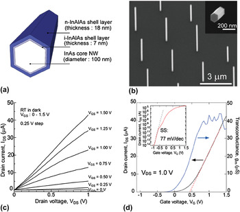
Figures 12(c) and 12(d) plot the output and transfer characteristics of the device. The leakage current was dramatically decreased to 10−14 A/μm and the on–off ratio I ON/I OFF was approximately 109. Maximum drain current I ds,max was 23.3 μA (at V DS = 1 V) and peak transconductance g m,max was 43.0 μS (at V DS = ∼1 V). The V TH was 0.4 V. The I ds,max and g m,max were ∼10 times those of the NW-VSGTs using bare InAs NWs. These improvements resulted from the passivation effect of the InAlAs layer. We obtained a μ FE of 488 cm2/Vs. The minimum SS was 77 mV/decade, and the average subthreshold swing was about 142 mV/decade with a V G window of 1 V. These switching behaviors of SS properties close to the performance of very recent InGaAs-based multi-gate FinFETs.Reference Radosavljevic, Dewey, Fanstenau, Kavalieros, Kotlayer, Chu-Kung, Liu, Lubyshev, Metz, Millard, Mukherjee, Pan, Pillarisetty, Rachmady, Shah and Chau92
Although the switching performances of these multi-channel NW-VSGTs on Si were satisfactory for future III-V channels on Si platforms, mobility was still low. This is because of high series resistance resulting from source and drain contact. It is necessary to optimize the doping density of the Si substrate and InAs NWs through band engineering to further minimize the effect of high source resistance and to form a source electrode directly on the bottom of the NWs. In addition, the field-effect mobility was reduced, neglecting series resistance including access resistance by the potential barrier at the Si/InAs interface. Interface states still reduced transconductance and lowered the estimated value of field-effect mobility. Further improvements and optimization of the doping concentration are required to reduce such degradation.
IV. CONCLUSIONS
We have reviewed recent progress in III-V NWs grown by SA-MOVPE and that in III-V NW-based device applications. This technique enabled position-controlled and vertically aligned growth of III-V NWs on lithography patterned substrates. Also, the growth temperature altered the directions of axial growth and radial NW growth and resulted in formation of CMS NWs. Moreover, the nanometer-scaled footprint and precise control of the initial surface with SA-MOVPE achieved to integrate III-V NWs with Si substrates.
Using the CMS structure and growing these III-V NWs enabled us to fabricate CMS NW–based LEDs, solar cells, and NW-VSGTs. Vertically aligned AlGaAs/GaAs/AlGaAs DH CMS with radial p-n junctions were successfully fabricated. Then, NW-LEDs using these CMS NWs exhibited moderate rectifying properties and EL with wavelengths from 820–870 nm. These NW-LEDs in the NIR should open new approaches toward Si photonics because nanometer-scaled light sources at NIR are feasible for Si-based avalanche photodiodes (APDs) to replace Cu-based intra-chip connections with high-performance optical interconnections in small areas. We fabricated core-shell p-n junction NWs for photovoltaic applications by the combining axial and lateral epitaxial growth in SA-MOVPE. A photovoltaic device was fabricated using a periodical aligned array of NWs and it demonstrated 3.37% efficiency. We successfully integrated vertical InAs NWs and InAs/InAlAs CMS NWs on Si substrates for electronic devices. The NW-VSGTs demonstrated excellent switching behavior, which was on the same level of technology as novel III-V–based FinFETsReference Radosavljevic, Dewey, Fanstenau, Kavalieros, Kotlayer, Chu-Kung, Liu, Lubyshev, Metz, Millard, Mukherjee, Pan, Pillarisetty, Rachmady, Shah and Chau92 toward fast III-V channel on future Si-CMOS. The NW-VSGTs had issues with carrier mobility and miniaturization. Further improvements such as modulation doping are required for future application.
We still face challenges in future devices using III-V NWs. We have to develop the technologies discussed in this study into low power–driven transistor such as tunnel FET (TFET),Reference Björk, Knoch, Schmid, Riel and Riess93 high-electron mobility channels such as high-electron mobility transistors (HEMTs), electrically driven NW-based laser diodes (LDs), III-V NW-based photodiodes, APDs,Reference Chuang, Sedgwick, Chen, Ko, Moewe, Ng, Tran and C-Hasnain64 and solar cells with high energy efficiency. It is necessary to optimize device structures and doping conditions to achieve these devices. Moreover, new concepts such as metal cavities with surface plasmonicsReference Kwon, Kang, Seassal, Kim, Regreny, Lee, Lieber and Park94, Reference Im, Lindquist, Lesuffleur and Oh95 and band discontinuityReference Wei, Bao, Soci, Ding, Wang and Wang78, Reference Björk, Schmid, Bessire, Moselundm, Ghoneim, Karg, Lörtscher and Riel96, Reference Tomioka and Fukui97 should be considered for new applications. After optimization and realization of NW-based TFET, HEMT, LDs, APDs, and solar cell, these NW-based optical applications should open up new fields in future NW-based technology.
ACKNOWLEDGMENTS
The authors thank Drs. Junichiro Takeda, Premila Mohan, Lin Yang, Ying Ding, Takuya Sato, and Mr. Masatoshi Yoshimura, Yasunori Kobayashi, Tomotaka Tanaka, and Hajime Goto. This work was financially supported by a Grant-in-Aid for Scientific Research from the Ministry of Education, Culture, Sports, Science and Technology (MEXT) and the Japan Science and Technology Agency (JST) PRESTO program.