Introduction
Reconfigurableantennas are highly needed for modern wireless communication applications due to there several advantages such as adaptability, improved system performance, size reduction, cost savings, enhanced coverage, improved capacity, etc. [Reference Sharma and Chieh1]. Reconfigurable antennas have the capability to modify operational parameters such as frequency [Reference Chen, Hao-Zhan, Wong, Wei, Ren and Yuan2], pattern [Reference Yuan, Huang, Zhang, Cui, Weiwei and Yuan3], and polarization [Reference Mei, Zhang, Tang, Zhu and Liu4]. In the last decade, reconfigurable antenna designs have been proposed in the literature, achieving single-parameter or multi-parameter reconfiguration [Reference Khairnar, Ramesha and Gudino5].
Due to the mutual interaction between antenna elements, phased arrays often experience significant gain changes, particularly at lower elevation angles [Reference Khairnar, Kadam, Ramesha and Gudino6]. Pattern reconfigurable antennas need the capability to manipulate both the direction and shape of their radiation pattern to fulfill the increasing demands of future wireless communication systems. To improve signal reception and reduce interference, beam steering antennas can focus main beam of the antenna toward a particular direction. In contrast, beam shaping antennas possess the capacity to switch among various radiation patterns, encompassing omnidirectional, directional, conical, and bidirectional radiation patterns. This provides a wide range of possibilities that may be adapted to a variety of communication scenarios [Reference Pablo Zapata Cano, Zaharis, Yioultsis, Kantartzis and Lazaridis7].
Pattern reconfigurable antennas with beam steering capability makes use of diverse technologies such as tunable parasitic elements [Reference Ouyang and Gong8], leaky wave antennas [Reference Geng, Wang, Yujian, Zheng, Chen and Zhang9], partially reflecting surfaces (PRSs) [Reference Lu-Yang, Zhang and Liu10], liquid metal magnetoelectric dipole [Reference Geng, Ming, Zhang, Wang, Pan, Chen and Liu11], etc. It is important to note that the aforementioned designs are able to alter the main beam within a restricted scanning range. However, certain applications require a radiation beam that can switch between opposite directions. While there has been extensive research on the reconfiguration of radiation patterns, the exploration of multibeam capabilities has been comparatively less reported. The need for antennas capable of switching the radiation beam between opposite directions highlights a distinct challenge that may require further investigation and development in the field [Reference Xuan, Huitema and Wong12].
The design approaches used to achieve the multibeam characteristics in pattern reconfigurable antennas include dipole antennas [Reference Ren, Yang, Yin and Yin13, Reference Prakash, Kumar Chaudhary and Kumar Gangwar14], monopole antenna [Reference Ding and Wang15], slot antennas [Reference Prakash, Kumar Chaudhary and Kumar Gangwar14, Reference Shamsinejad, Khalid, Monavar, Shamsadini, Mirzavand, Moradi and Mousavi16–Reference Prakash, Kumar Chaudhary and Kumar Gangwar19], and patch antennas with shorting pins [Reference Cao, Zhang, Xiaona and Wang20, Reference Lu and Yang21]. The antenna design outlined in [Reference Ren, Yang, Yin and Yin13] utilizes H-shaped resonator structures to attain reconfigurable patterns. This antenna can switch between the broadside and endfire patterns. It achieves a 16% impedance bandwidth, spanning from 2.47 to 2.9 GHz. This antenna has the advantage of providing high gain, a high front-to-back ratio, and a wide operational bandwidth. The pattern reconfigurable antenna design presented in [Reference Prakash, Kumar Chaudhary and Kumar Gangwar14] provides four single beams broadside, backside, endfire, and backfire. This antenna is also able to provide two bidirectional patterns. The antenna makes use of H-shaped slot with reconfigurable reflecting surfaces placed on the top and bottom side. A reconfigurable switching network consisting of single pole three throw (SP3T) is used. A wideband pattern reconfigurable antenna, comprising a monopole as the driven element and parasitic antenna elements serving as directors is presented in [Reference Ding and Wang15]. This antenna is capable of generating two endfire patterns and one broadside pattern within the C band, demonstrating an overall bandwidth of 29%. The pattern reconfigurable cubic slot antenna, as proposed in [Reference Shamsinejad, Khalid, Monavar, Shamsadini, Mirzavand, Moradi and Mousavi16], can switch its radiation pattern between omnidirectional and broadside radiation at an operating frequency of 2.4 GHz. This feature makes it well suited for applications in wireless sensor networks. The antenna achieves a peak gain of 2.85 dBi and 4.2 dBi, with −10 dB impedance bandwidths of 21% and 1.7% for the omnidirectional and broadside radiation, respectively. The antenna has a few limitations, including a non-planar design and varying operating bandwidths for the two operational modes. A compound reconfigurable antenna with frequency, radiation pattern, and polarization agility is discussed in [Reference Lei, Yujian, Wang and Sim17]. This antenna is capable of producing radiation pattern in forward and backward directions. A planar antenna featuring vertical polarization, providing both omnidirectional and unidirectional pattern diversity is discussed in [Reference You and Dong18]. This antenna operates in two modes, exhibiting a 3.3% overlapping −10 dB impedance bandwidth and achieving a peak gain of 1.8 dBi. The antenna design presented in [Reference Prakash, Kumar Chaudhary and Kumar Gangwar19] is capable of adjusting its radiation pattern, half-power beamwidth, and supporting multibeam functionality. The antenna allows for seamless reconfiguration between single and multibeam radiation along the ±z direction. It exhibits a 6.18% bandwidth overlap with an average gain of 8.32 dBi. A pattern reconfigurable bidirectional antenna is explored in [Reference Cao, Zhang, Xiaona and Wang20]. This antenna operates in three distinct states, offering a broadside and backward radiation pattern in state 1. In state 2, backfire and endfire radiation patterns are achieved, while state 3 yields quad-beam patterns. The antenna features a 2% overlapping −10 dB impedance bandwidth and attains a peak gain of 7.3 dBi. In [Reference Lu and Yang21], a circular driven patch is presented, capable of omnidirectional and endfire patterns in three distinct states. The antenna achieves a peak gain of 6.34 dBi.
Through an in-depth literature review, it is evident that there is limited coverage in the literature regarding pattern reconfigurable antennas with multibeam radiation capabilities. Certain applications specifically require antennas with the ability to produce multiple beams, indicating a gap in current research. Further investigation and development are necessary to design pattern reconfigurable antennas capable of multibeam radiation. Additionally, it has been observed that reported multibeam antennas often exhibit narrow impedance bandwidth and low gain. To address this limitation, pattern reconfigurable antennas with multibeam radiation capabilities should aim to achieve a broader range of radiation patterns, a larger operating bandwidth, high gain, a low profile, a simple design, a reduced number of active components, and efficient DC signal control circuitry.
This paper introduces a pattern reconfigurable antenna featuring a novel structure comprising a cross-slot antenna and an active PRS layer. The designed cross-slot antenna exhibits a bidirectional radiation pattern. The reconfigurable PRS layer comprises a 4×4 array of PRS unit cells loaded with PIN diodes to facilitate beam transition between different directions. Modifying states of these PIN diodes allows for the generation of broadside, backfire, and bidirectional radiation patterns. The proposed antenna achieves an overlapped fractional bandwidth of 21.83% with a peak gain of 9.60 dBi. This is achieved with a compact size of  $0.81\lambda_0\times0.81\lambda_0\times0.59\lambda_0$. Rest of this paper is organized as follows:Section antenna design and working principle provides the proposed antenna design and working principle. Section results and discussion presents detailed simulated and measured results. Finally, Section conclusion concludes the paper.
Antenna design and working principle
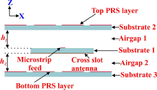
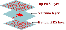
The antenna design consists of three layers, incorporating a central cross-slot antenna complemented by a 4×4 active PRS unit cell array situated both at the top and bottom. This configuration is illustrated in Figs. 1 and 2. A microstrip feed is located on the upper surface of substrate 1, while a cross-slot is located on its lower surface. In addition, reconfigurable PRS layers are placed on the upper surfaces of substrate 2 and substrate 3. An air gap with a height denoted as h 1 = 23 mm separates the top PRS layer from the cross-slot antenna. Similarly, another air gap with a height denoted as h 2 = 23 mm separates the bottom PRS layer from the cross-slot antenna. In this section, we discussed the design of the unit cell, the cross-slot antenna, the PRS layer, and the working principle. To design the cross-slot antenna and PRS layer, an FR4 substrate (ϵr = 4.5, h = 1.6 mm, and  $\tan\delta$ = 0.02) is used. The proposed antenna is simulated using Ansys High Frequency Structure Simulator (HFSS) software [22].
Cross-sectional view of the proposed antenna.

Isometric view of the proposed antenna.

Unit cell
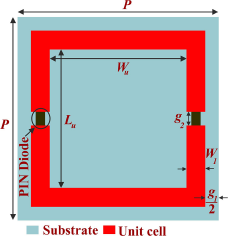
Geometrical design of the proposed unit cell is illustrated in Fig. 3. It comprises a single square loop shape with four arms, each having a PIN diode on both its left and right sides. The optimized unit cell dimensions are as follows (in millimeters): periodicity P = 15, inner square patch length Lu = 10.2, inner square patch width Wu = 10.2, square loop width W 1 = 1.4, gap between unit cells g 1 = 2, and gap to connect PIN diode in the square loop g 2 = 1.
Geometrical design of the unit cell.

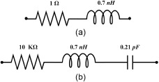
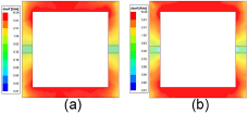
Skyworks SMP1340-079LF PIN diodes, known for their fast switching speed, low capacitance, and plastic packaging are integrated into the proposed unit cell design [23]. The equivalent circuit models for the ON and OFF states of the PIN diode are displayed in Fig. 4(a) and (b) respectively. In HFSS, modeling of the PIN diodes involves considering a lumped RLC boundary. The unit cell current distributions are depicted in Fig. 5(a) and (b). In both states, the current exhibits the highest intensity along the horizontal strips of the square loop.
PIN diode equivalent circuit model (a) ON state and (b) OFF state.

Simulated current distribution of the proposed unit cell (a) ON state and (b) OFF state.

The transmission and reflection analysis of the proposed unit cell is performed using Ansys HFSS. The unit cell is simulated with periodic boundary conditions and applying Floquet ports to extract the scattering parameters, reflection coefficient  $|S_{11}|$ and transmission coefficient
 $|S_{21}|$. The
 $|S_{11}|$ represents portion of the incident wave reflected back from the unit cell, while
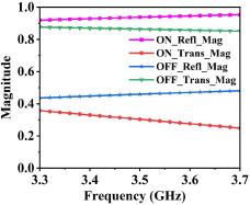
 $|S_{21}|$ represents portion transmitted through the unit cell. Figure 6 shows the magnitudes of transmission and reflection for the unit cell in the PIN diode ON and OFF states. At 3.5 GHz, when the PIN diode is ON, the reflection and transmission magnitudes are 0.938 and 0.30 respectively. When the PIN diode is OFF, the reflection and transmission magnitudes are 0.459 and 0.864 respectively. Therefore, from Fig. 6, we can conclude that the unit cell acts as a reflective surface when the PIN diode is ON and as a transmissive surface when the PIN diode is OFF.
Simulated magnitude characteristics of the proposed unit cell.

Cross-slot antenna design
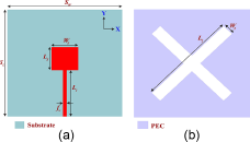
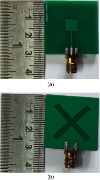
The radiating element comprises a cross-slot antenna with microstrip line feeding. Figure 7(a) and (b) illustrate top and bottom views of the cross-slot antenna radiator. The proposed antenna possesses the following dimensions expressed in millimeters. The substrate dimensions include a length (SL) of 29.5 and a width (SW) of 29.5. The feed line dimensions consist of a length (L 1) of 14.75 and a width (fw) of 1. The stub is defined by a length (LS) of 6.4 and a width (WS) of 6.9. Additionally, the cross-slot dimensions are a length (L 2) of 25.8 and a width (W 2) of 3, with an angle between the cross-slots set at 60∘.
Cross-slot antenna. (a) Top view and (b) bottom view.

The PRS layer design
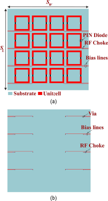
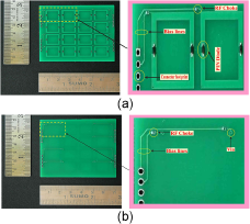
The PRS layer is composed of an array of 4×4 unit cells. Figure 8(a) presents the top view of this layer, while Fig. 8(b) illustrates the bottom view. The complete 4×4 PRS unit cell layer is fabricated on an FR4 substrate, with dimensions of SL = 70 mm (length) and SW = 70 mm (width). The PRS layer achieves reconfigurability through the incorporation of PIN diodes in unit cell. The orientation of the PIN diodes is uniform in both PRS layers. DC voltage is applied to these PIN diodes through 0.3 mm thin metallic biasing striplines on each row of unit cells. A specialized DC biasing control circuit is utilized to apply bias voltage. This unique circuitry guarantees accurate regulation of the DC voltage across the PIN diodes in the PRS layer. To simplify and optimize biasing efficiency, the grounding for all PIN diodes is strategically located on the bottom side of the PRS layer. This arrangement streamlines the biasing circuitry while maintaining effective grounding for the PIN diodes. As shown in Fig. 8(b), a via connection is utilized to connect the grounding to the top biasing lines. The purpose of adopting this arrangement is to prevent unnecessary complexity in the biasing circuitry. To mitigate the impact of RF current, 13.5 nH surface-mounted RF choke inductors are strategically incorporated within the biasing lines, aligning with established practices for minimizing RF interference [24].
Active 4×4 PRS layer. (a) Top view and (b) bottom view.

Working principle
To enable pattern reconfiguration, PIN diodes are loaded on both the top and bottom PRS layer. The PRS layer generates more reflection and less transmission when its PIN diodes are ON. In contrast, more transmission and less reflection are provided by the PRS when the PIN diodes connected to this PRS layer are OFF. Table 1 presents three different operating states that are used to explain the operational concept of the proposed antenna.
Operating states of the proposed antenna

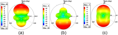
In state 1, PIN diodes attached to the top PRS layer are turned OFF, while the bottom PRS layer is turned ON, resulting in a broadside radiation pattern. State 2 is the opposite of State 1, resulting in a backward radiation pattern. In state 3, there is a bidirectional radiation pattern because the PIN diodes that are connected to the top and bottom PRS layers are in the OFF state. Figure 9 shows simulated 3D polar radiation patterns at 3.5 GHz for states 1, 2, and 3.
3D radiation pattern at 3.5 GHz for (a) state 1, (b) state 2, and (c) state 3.

Results and discussion
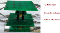
This section provides comprehensive simulated and measured results. The top view of the fabricated cross-slot antenna is shown in Fig. 10(a), while the bottom view is depicted in Fig. 10(b). Similarly, the top view of the fabricated prototype of the PRS layer is displayed in Figure 11(a), and its bottom view is presented in Fig. 11(b). Figure 12 showcases the assembled cross-slot antenna featuring both top and bottom PRS layers. The suggested antenna performance is tested in a far-field anechoic chamber, as shown in Fig. 13.
Fabricated prototype of the cross-slot antenna. (a) Top view and (b) bottom view.

Fabricated prototype of the 4×4 PRS layer. (a) Top view and (b) bottom view.

Fabricated cross-slot antenna with top and bottom PRS layers.

Antenna measurement setup in the far-field anechoic chamber.

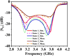
Performance of the proposed antenna has been simulated and measured in three distinct operating states. Figure 14 illustrates the simulated and measured reflection coefficients of the antenna structure for these three radiating states. In state 1, the simulated and measured −10 dB impedance bandwidth spans from 3 to 3.88 GHz, with a fractional bandwidth of 25.58%. In state 2, the −10 dB impedance bandwidth, both simulated and measured, ranges from 2.98 to 3.87 GHz with a fractional bandwidth of 25.98%. Moving to state 3, the −10 impedance bandwidth extends from 3.10 to 3.86 GHz, as observed in both simulated and measured results with a fractional bandwidth of 21.83%.
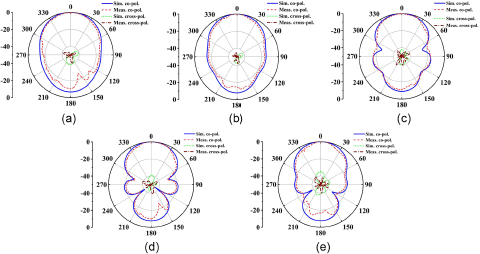
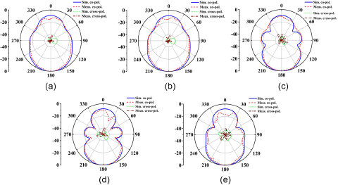
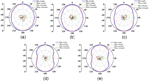
The antenna performs multibeam switching in the yz-plane. Figs. 15, 16, and 17 show normalized simulated and measured radiation patterns for states 1, 2, and 3 at different frequencies. In state 1, the antenna produces broadside radiation. The achieved peak gain is 9.60 dBi with an efficiency of 84.29%. In state 2, the antenna emits backward radiation. The achieved peak gain is 9.52 dBi with an efficiency of 84.68%. In state 3, it emits bidirectional radiation. The achieved peak gain is 5.87 dBi with an efficiency of 84.27%. Thus, the suggested antenna performs multibeam switching, producing broadside, backward, and bidirectional radiation patterns in states 1, 2, and 3 with an overlapped bandwidth of 3.10–3.86 GHz.
Table 2 compares performance of the proposed antenna with other reported works [Reference Ren, Yang, Yin and Yin13–Reference Lu and Yang21]. The antenna introduced in [Reference Ren, Yang, Yin and Yin13] demonstrates two radiation patterns (broadside and endfire) across three operational states, achieving a 15.2% overlapping −10 dB impedance bandwidth and 6.4 dBi gain. In [Reference Prakash, Kumar Chaudhary and Kumar Gangwar14], the antenna offers four radiation patterns (broadside, backside, endfire, and backfire) across three states, achieving an 8.9% overlapping −10 dB impedance bandwidth and 5.8 dBi gain. Similarly, the antenna in [Reference Ding and Wang15] exhibits broadside and endfire patterns across three states, achieving a 29% overlapping −10 dB impedance bandwidth and 7.4 dBi gain. In [Reference Shamsinejad, Khalid, Monavar, Shamsadini, Mirzavand, Moradi and Mousavi16], an antenna is presented with omnidirectional and directional patterns in two modes, featuring a 2.7% overlapping −10 dB impedance bandwidth and 4.2 dBi gain. Likewise, [Reference Lei, Yujian, Wang and Sim17] features an antenna with forward and backward radiation patterns in two states, offering a 3.5% overlapping −10 dB impedance bandwidth and 4 dBi gain. The antenna design presented in [Reference You and Dong18] provides omnidirectional and unidirectional patterns in two modes, with a 3.3% overlapping −10 dB impedance bandwidth and a 1.8 dBi gain. In [Reference Prakash, Kumar Chaudhary and Kumar Gangwar19], multiple radiation patterns are obtained with an overall bandwidth of 6.18%. Additionally, the antenna in [Reference Cao, Zhang, Xiaona and Wang20] offers broadside, backside, endfire, and backfire patterns across three states, featuring a 2% overlapping −10 dB impedance bandwidth and 7.3 dBi gain. Finally, [Reference Lu and Yang21] presents an antenna with omnidirectional and endfire patterns in three states, achieving a 6.34 dBi gain. It is apparent that the antennas discussed in previous studies exhibit limited −10 dB impedance bandwidth and moderate gain, which restricts their applications. In contrast, the proposed antenna demonstrates superior bandwidth and high gain, along with a compact size, making its suitability for sub-6 GHz applications.
Simulated and measured reflection coefficient of the proposed antenna structure for state 1, state 2, and state 3.

Simulated and measured normalized radiation patterns of state 1 in yz-plane (a) 3.1 GHz, (b) 3.3 GHz, (c) 3.5 GHz, (d) 3.7 GHz, and (e) 3.85 GHz.

Simulated and measured normalized radiation patterns of state 2 in yz-plane (a) 3.1 GHz, (b) 3.3 GHz, (c) 3.5 GHz, (d) 3.7 GHz, and (e) 3.85 GHz.

Simulated and measured normalized radiation patterns of state 3 in yz-plane (a) 3.1 GHz, (b) 3.3 GHz, (c) 3.5 GHz, (d) 3.7 GHz, and (e) 3.85 GHz.

Performance comparison of the proposed wideband and multibeam pattern reconfigurable antenna with other reported works

Conclusion
A novel pattern reconfigurable antenna is presented, consisting of a wideband cross-slot antenna and a reconfigurable PRS layer. The PRS layer includes PIN diodes, which can be used to achieve different radiation patterns by changing their states. The antenna operates in three states, producing broadside, backward, and bidirectional radiation patterns. A prototype of the pattern reconfigurable antenna has been fabricated and tested. Measured results show pattern reconfigurability from 3.10 to 3.86 GHz with a peak gain of 9.60 dBi. The proposed antenna offers increased bandwidth and high gain, and its compact size enhances its suitability for sub-6 GHz applications.
Data availability statement
No data were used for the research described in the article.
Author contributions
All authors contributed equally to design and development of design, reaching conclusions, and in writing the paper.
Competing interests
The authors report no competing interests.

Venkataswamy Suryapaga (Student Member, IEEE) received the B.Tech degree in Electronics and Communication Engineering from Bapatla Engineering College, Bapatla, Andhra Pradesh, India in 2004 and the M.Tech. degree in Digital Electronics and Communication Systems from QIS College of Engineering, Ongole, Andhra Pradesh, India in 2010. He is currently Internal Full Time research scholar with the School of Electronics Engineering (SENSE), at VIT-AP University, Amaravati. His research interests include design of Reconfigurable Antennas using metamaterials for 5G and beyond applications.

Vikas V. Khairnar (Member, IEEE) received a B.E. degree in Electronics & Telecommunication Engineering from Savitribai Phule Pune University, India, in 2009. He obtained his M.E. in Communication Engineering from Dr. BAMU University, India, in 2013. He received the Ph.D. degree from BITS Pilani, India, in 2020. He is currently working as an Assistant Professor with the School of Electronics Engineering (SENSE), VIT-AP University, Amaravati, Andhra Pradesh, India. His research area includes the design of reconfigurable antennas, antenna arrays, and metasurface inspired antennas.