Introduction
A memory device composed of organic materials sandwiched between two electrodes possesses at least two stable resistance states controlled by an external electrical stimulus.Reference Yang, Ouyang, Ma, Tseng and Chu1–Reference Ling, Liaw, Zhu, Chan, Kang and Neoh3 Organic materials provide many advantages, including simple device structures, low fabrication costs, printability, and flexibility. The device resistance states can be read nondestructively, and no electrical power is required to maintain the states, indicating a nonvolatile memory.Reference Yang, Ouyang, Ma, Tseng and Chu1–Reference Ling, Liaw, Zhu, Chan, Kang and Neoh3 Furthermore, essential requirements for high performance memory, such as a high ON/OFF ratio, long endurance and retention characteristics, and a fast switching speed, have been experimentally verified.Reference Ouyang, Chu, Szmanda, Ma and Yang4, Reference Mukherjee and Pal5 Although it is difficult to identify the device operating mechanisms, in-depth studies of charge conduction mechanisms have contributed to the device physics that underlies the switching phenomena. Structural and electrical optimizationsReference Mukherjee and Pal5, Reference Lin and Ma6 have also been applied successfully to improve device performance. The main focus of this review is to provide a general summary about the materials, structures, characteristics, and mechanisms of organic resistive memory devices. We also introduce several critical strategies for device integration and advanced circuit architectures.
Materials, structures, and characteristics of organic switching devices
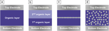
An organic resistive memory device consists of organic layers sandwiched between bottom and top electrodes. Various organic materials have shown switching resistances in response to applied voltages.Reference Yang, Ouyang, Ma, Tseng and Chu1, Reference Chu, Ouyang, Tseng and Yang7–Reference Bandyopadhyay and Pal36 Organic materials that exhibit conductance switching include small molecules,Reference Donhauser, Mantooth, Kelly, Bumm, Monnell, Stapleton, Price, Rawlett, Allara, Tour and Weiss17–Reference Das and Pal20, Reference Bandyopadhyay and Pal36 polymers,Reference Yang, Ouyang, Ma, Tseng and Chu1, Reference Carchano, Lacoste and Segui21–Reference Kim, Yook, Jang and Lee27 and composites containing nanoparticles (NPs).Reference Lai and Chen8–Reference Liu, Ling, Kang, Neoh, Liaw, Chang, Zhu and Chan10, Reference Laiho, Majumdar, Baral, Jansson, Osterbacka and Ikkala28–Reference Son, Kim, Park, Choi, Li, Ham and Kim35 Specifically, the conductance switching of single and bundled phenylene ethynylene oligomers isolated in matrices of alkanethiolate monolayers was caused by conformational changes in the molecules or bundles.Reference Donhauser, Mantooth, Kelly, Bumm, Monnell, Stapleton, Price, Rawlett, Allara, Tour and Weiss17 A reliable nonvolatile memory device using a polyfluorene-derivative single-layer film has been characterized.Reference Kim, Oh, Choi, Wang, Hwang, Kim and Lee24 Nonvolatile resistive memory effects of gold nanoparticles embedded in the conducting polymer poly(4-n-hexylphenyldiphenylamine) also has been investigated using admittance spectroscopy.Reference Simon, Griffo, DiPietro, Swanson and Carter31 In particular, the following four device structures have been implemented (Figure 1): (1) a single-layer structure containing only one type of organic material, (2) a bilayer structure containing two types of organic materials, (3) a trilayer structure in which nano-traps for charge carriers are sandwiched between two organic layers, and (4) spin-cast polymer-NP blends in which nano-traps are randomly distributed throughout the entire region of the host matrix. Among these device structures, the single-polymer-layer structure is more attractive due to the simplicity of device fabrication. Organic-based composite materials are commonly used to induce resistive switching.Reference Lai and Chen8–Reference Liu, Ling, Kang, Neoh, Liaw, Chang, Zhu and Chan10, Reference Laiho, Majumdar, Baral, Jansson, Osterbacka and Ikkala28–Reference Son, Kim, Park, Choi, Li, Ham and Kim35, Reference Cho, Kim, Choe, Wang, Song and Lee37 Polymer-blend systems containing organic or inorganic NPs mainly constitute the active materials of resistive memory devices. Resistance switching in these materials is caused by the introduction of NPs into the polymer matrix.Reference Lai and Chen8, Reference Cho, Yasue, Yoon, Lee, Yeo, Chung, Moon and Ryu9, Reference Li, Kim, Dong and Kim29–Reference Simon, Griffo, DiPietro, Swanson and Carter31, Reference Song, Ling, Lim, Teo, Tan, Li, Kang, Chan and Zhu33, Reference Son, Kim, Park, Choi, Li, Ham and Kim35, Reference Cho, Kim, Choe, Wang, Song and Lee37 The concentration and distribution of NPs in a blend system are important fabrication factors and must be carefully controlled during solution preparation.Reference Lai and Chen8, Reference Liu, Ling, Teo, Zhu, Chan, Neoh and Kang11, Reference Laiho, Majumdar, Baral, Jansson, Osterbacka and Ikkala28, Reference Cho, Kim, Choe, Wang, Song and Lee37 The active matrix architectureReference Cho, Kim, Song, Ji, Jo, Hwang, Jung and Lee38–Reference Baek, Kim, Lee, Kim, Yim, Lee, Lee, Ahn, Seo, Lee, Park, Cha, Park, Kim, Yoo, Chung, Moon and Ryu41 (i.e., crossbar organic resistive memory combined with a diode or transistor) is also essential for practical memory applications.
Typical structures of organic memory cells: (a) a single-layer structure without nanoparticles (NPs), (b) a bilayer structure containing two kinds of polymers, (c) a structure with nano-traps buried in the middle of an organic layer, and (d) a polymer-NP composite with NP traps randomly distributed throughout the entire host polymer.Reference Ling, Liaw, Zhu, Chan, Kang and Neoh3

Mechanisms of resistive switching
The conduction mechanism in organic materials is complex because the amorphous structure of the organic materials cannot be explained adequately on the basis of ordered inorganic materials.Reference Nalwa42 The conduction in organic materials is normally explained by intrinsic charge carrier generation in the organic materials and charge carrier injection from electrodes to organic materials. Intrinsic carrier density in organic materials is usually very low, and carriers are usually trapped by localized states, which makes it difficult to understand charge transport behavior. A number of conduction mechanisms such as Ohmic conduction, Schottky emission, thermionic emission, space charge-limited current (SCLC), tunneling current, ionic conduction, hopping conduction, and impurity conduction have been utilized to explain the conduction process in organic materials.Reference Ling, Liaw, Zhu, Chan, Kang and Neoh3
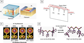
When the current in the ON state is highly localized to a small fraction of the device area, the conduction phenomenon is called filamentary conduction (Figure 2a).Reference Dearnaley, Morgan and Stoneham43, Reference Dearnaley, Stoneham and Morgan44 Two kinds of filamentary conduction have been suggested: One is associated with the carbon-rich filaments formed by the local degradation of organic films.Reference Pender and Fleming45, Reference Segui, Ai and Carchano46 The other is related to the metallic bridges that result from the migration of electrodes.Reference Dearnaley, Morgan and Stoneham43, Reference Hwang and Kao47 When filaments are formed in an organic device, the ON state shows temperature-independent electrical behavior or metallic I–V characteristics.Reference Henisch and Smith22 It also exhibits a device area-independent behavior, which is due to the formation of much smaller filaments.Reference Henisch and Smith22, Reference Segui, Ai and Carchano46 Highly localized current images of ON state materials have also been used to support filamentary switching mechanisms.Reference Kim, Oh, Choi, Wang, Hwang, Kim and Lee13 As an example of filamentary switching, Cu ions that penetrated into a poly(3-hexylthiophene) (P3HT) layer under forward bias resulted in filament formation in a Cu/P3HT/Al device, which was experimentally observed by secondary ion mass spectroscopy analysis.Reference Joo, Choi, Lee and Chung48 Similar metallic filaments were also formed in poly(ethylenedioxythiophene): poly(styrenesulfonate) (PEDOT:PSS) or poly(4-hydroxystyrene) composite materials that contain homogeneously dispersed Au clusters.Reference Sivaramakrishnan, Chia, Yeo, Chua and Ho49 Nanoscale memory devices can be easily achieved in filamentary-based systems because switching is possible even in highly localized regions.
Schematics to illustrate the mechanisms for organic resistive switching induced by (a) filamentary conduction (M represents metal, and I represents insulator),Reference Waser and Aono88 (b) space-charge-limited-conduction (where red dots represent electrons), (c) charge transfer-based conduction,Reference Ling, Lim, Song, Zhu, Chan, Kang and Neoh89 and (d) conformation change-based switching induced by changes in electric field polarity.Reference Xie, Ling, Hou and Huang90

Another switching mechanism is related to SCLC. For instance, a trap-filled SCLC model was proposed to explain the resistive switching effect in Al/polystyrene (PS) + Au NPs/Al device (seen in Figure 2b). Therefore, Au NPs were treated as traps in the PS. When the electrode/organic material contact is Ohmic, the accumulation of carriers near the electrode builds up a space charge. Mutual repulsion between individual charges restricts the total charge injected into the organic material, resulting in SCLC.Reference Carbone, Kotowska and Kotowski50, Reference Mark and Helfrich51 The electrical switching in some organic materials has been reported to be associated with space charges and SCLC.Reference Majumdar, Bandyopadhyay, Bolognesi and Pal25 For example, hysteresis characteristics in the I–V curves of a ITO/poly [3-(6-methoxyhexyl)thiophene] (P30Me)/Al structure were observed.Reference Majumdar, Bandyopadhyay, Bolognesi and Pal25 Space charges accumulate at the metal/polymer interfaces and induce SCLC.Reference Das and Pal52 The stored charges control charge injection and lead to hysteresis in the I–V curve. It is also observed that current abruptly increases at a threshold voltage, reaches the maximum value, and then passes through a negative differential region to the minimum value. It was proposed that the active mechanism is similar to that observed in inorganic metal-insulator-metal diodes by Simmons and Verderber.Reference Simmons and Verderber53 Indeed, similar switching behaviors have been reported for many different materials in the same trilayer structure,Reference Bozano, Kean, Beinhoff, Carter, Rice and Scott12, Reference Reddy, Karak and Dhar54, Reference Park, Nam, Seo, Kim, Oh, Lee and Paik55 which provides insights into the switching mechanisms.
Switching may also be induced by charge transfer-based (Figure 2c) and conformation change-based conduction (Figure 2d). Charge transfer (CT) occurs in electron donor-acceptor systems in which electrical charges are partially transferred from the donor to the acceptor moiety.Reference Chu, Ouyang, Tseng and Yang7, Reference Liu, Ling, Kang, Neoh, Liaw, Chang, Zhu and Chan10, Reference Song, Ling, Lim, Teo, Tan, Li, Kang, Chan and Zhu33, Reference Potember, Poehler and Cowan56 The electrical memory effect of CT complexes was observed in Cu-tetracyanoquinodimethane (TCNQ),Reference Potember, Poehler and Cowan56 where Cu is the donor and TCNQ is the organic acceptor. Raman spectroscopy showed that the TCNQ anions in the pristine high resistance film were replaced by neutral TCNQ molecules in the low resistance state.Reference Kamitsos, Tzinis and Risen57 Chu et al.Reference Chu, Ouyang, Tseng and Yang7 also observed that the bistable resistance states of a [6,6]-phenyl-C61-butyric acid methyl ester (PCBM) and tetrathiofulvalene (TTF) dispersed in a polystyrene matrix were due to a charge transfer effect between the TTF and PCBM in the film. A strong electric field facilitated the transfer of electrons from the highest occupied molecular orbital of TTF to the lowest unoccupied molecular orbital of PCBM, producing a positive charge in TTF and a negative charge in PCBM. A sharp increase in conductivity occurred after the charge transfer.Reference Chu, Ouyang, Tseng and Yang7
Conductance switching and memory effects of molecular electronic devices often arise from electrically or optically induced conformational changes in molecules or molecular bundles.Reference Donhauser, Mantooth, Kelly, Bumm, Monnell, Stapleton, Price, Rawlett, Allara, Tour and Weiss17, Reference Kronemeijer, Akkerman, Kudernac, Wees, Feringa, Blom and Boer58 For example, the Rose Bengal molecule in supramolecular matrices of polyelectrolytes has shown conductance switching.Reference Bandyopadhyay and Pal36 A similar effect was also proposed for the resistive switching of poly(2-(9H-carbazol-9-yl)ethyl methacrylate) (PCz) and poly(9-(2-((4-vinylbenzyl)oxy)ethyl)-9H-carbazole) (PVBCz), which are non-conjugated polymers containing electron-donating carbazole pendant groups.Reference Lim, Ling, Teo, Zhu, Chan, Kang and Neoh23, Reference Teo, Ling, Song, Tan, Wang, Kang, Chan and Zhu59 Upon application of an electric field, randomly oriented carbazole groups in the organic materials were rearranged into face-to-face conformations, thus facilitating carrier delocalization and transport and producing a high-conductance state. Ionic conduction-based resistive switching has been also reported.Reference Verbakel, Meskers and Janssen32, Reference Smits, Meskers, Janssen, Marsman and de Leeuw60 Perhaps, the exact switching mechanisms may depend on the organic materials used, that is, a unified switching model to describe the switching mechanism of various organic materials does not exist, and more than one switching mechanism might work simultaneously in an organic memory device.
Device performance and requirements
The performance of memory devices is specified by their storage capacity, ON/OFF ratio, speed to write or erase, cycling endurance, retention time, and fabrication cost. The value of the ON/OFF ratio determines whether or not the circuitry can distinguish between high and low resistance values. Researchers usually emphasize the value of the ON/OFF ratio measured in single cells, but the statistical distribution of the ratios measured from many cells over many cycles should be considered to be more important. Narrow distribution of the resistances at each state and large gap between the states are considered to be necessary and challenging for organic memory circuits.
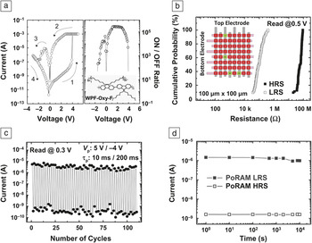
The series of plots shown in Figure 3 demonstrate typical nonvolatile memory performance of organic memory devices fabricated using a single layer of polyfluorene-derivative (denoted as WPF-oxy-F, chemical structure shown in the inset of Figure 3a) film. Figure 3a shows I–V data measured from an organic memory device using a single layer of WPF-oxy-F film (left plot of Figure 3a),Reference Kim, Oh, Choi, Wang, Hwang, Kim and Lee24 which shows bipolar nonvolatile memory behavior with an ON/OFF ratio of ∼10Reference Ling, Liaw, Zhu, Chan, Kang and Neoh3 at 0.3 V (right plot of Figure 3a). Figure 3b is a cumulative plot showing device uniformity in memory arrays.Reference Kim, Lee, Oh, Wang, Kim, Jung and Lee61 The inset in Figure 3b schematically shows an array of memory devices with an 8 × 8 crossbar structure, where red cells represent 60 functional switchable cells, and green cells represent 4 non-switchable cells. The distributions of both ON (low resistance state [LRS]) and OFF (high resistance state [HRS]) are within an order of magnitude, and the difference between HRS and LRS was found to be more than two orders of magnitude.
Switching characteristics of WPF-oxy-F organic memory devices. (a) I–V characteristics (left) and ON/OFF ratio of resistances (right) are shown as a function of the applied voltage bias.Reference Kim, Oh, Choi, Wang, Hwang, Kim and Lee24 (b) Cumulative probability of the device resistances at their low resistance state (LRS) and high resistance state (HRS) measured from an 8 × 8 crossbar memory circuit.Reference Kim, Lee, Oh, Wang, Kim, Jung and Lee61 (c) Switching cycles of currents through a resistive switching device modified by consecutive voltage pulses. The device ON and OFF states were alternated with a 5 V pulse (writing process) and a −4 V voltage pulse (erasing process) with pulse duration times of 10 ms and 200 ms, respectively.Reference Kim, Choi, Oh, Jo, Wang, Cho, Kim, Hwang and Lee62 (d) The retention characteristics of a resistive switching device at its LRS and HRS (PoRAM: polymer random access memory).Reference Kim, Choi, Oh, Wang, Kim, Hwang and Lee63 The chemical structure of WPF-oxy-F is shown in the inset of (a).

The performance of organic memory devices is also evaluated in terms of sweep endurance, write-read-erase-read cycle tests, switching cycles with consecutive pulses, and retention tests. Figure 3c shows switching cycle data of a memory device measured with consecutive voltage pulses.Reference Kim, Choi, Oh, Jo, Wang, Cho, Kim, Hwang and Lee62 ON and OFF states were alternated with a 5 V pulse (writing) and a −4 V voltage pulse (erasing) with pulse duration times of 10 ms and 200 ms, respectively.Reference Kim, Choi, Oh, Jo, Wang, Cho, Kim, Hwang and Lee62 The typical time to write and erase conventional flash memory is several milliseconds. It is essential to develop fast organic memory systems that are rewritable in times of a microsecond or less. In this regard, some organic resistive memory devices have been demonstrated with a voltage pulse of tens of nanoseconds.Reference Ouyang, Chu, Szmanda, Ma and Yang4
Figure 3d shows retention characteristics, where the HRS and LRS values were sustained for 104 s without any significant degradation.Reference Kim, Choi, Oh, Wang, Kim, Hwang and Lee63 The memory retention is still not comparable to commercial nonvolatile memory devices, and significant research efforts are being devoted to improvements. Moreover, the device endurance cycles are typically limited to several hundreds to several thousands of cycles, which also limits their practical applications. This problem may arise from gradual electrical degradation by oxygen or moisture in air, and thus additional passivation or packaging processes may be a solution for this issue. The fabrication cost of organic memory is considerably cheaper than flash or other conventional silicon-based electronics because cost-effective fabrication processes such as spin-coating or printing are available for organic electronics.
Integrated circuit architectures
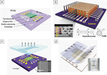
The crossbar structure is considered an ideal architecture for the integration of organic memory circuits (Figure 4a).Reference Kim, Lee, Oh, Wang, Kim, Jung and Lee61 All the overlapping regions between bottom (word lines) and top electrodes (bit lines) are referred to as information storage cells in this structure. However, a simple crossbar array in a passive matrix (called 1R array), including only information storage cells, has cross-talk interference that occurs because of the leakage of current paths (called sneak paths) through neighboring cells with low resistancesReference Lee, Park, Suh, Lee, Seo, Kim, Jung, Kang, Ahn, Lee, Seo, Cha, Yoo, Kim and Park39, Reference Baek, Kim, Lee, Kim, Yim, Lee, Lee, Ahn, Seo, Lee, Park, Cha, Park, Kim, Yoo, Chung, Moon and Ryu41 or an excess of current that may induce electrical damage.Reference Kinoshita, Tsunoda, Sato, Noshiro, Yagaki, Aoki and Sugiyama64 The solution to prevent cross-talk is to introduce a switching component (transistor or diode) to each cell.Reference Asadi, de Leeuw, de Boer and Blom16, Reference Cho, Kim, Song, Ji, Jo, Hwang, Jung and Lee38, Reference Kim, Choi, Oh, Wang, Kim, Hwang and Lee63, Reference Scott65 The International Technology Roadmap for Semiconductors (ITRS) also emphasized the combination of a diode or transistor with a resistor in a single chip.66 The architecture of one diode and one resistor (1D1R)Reference Cho, Kim, Song, Ji, Jo, Hwang, Jung and Lee38, Reference Lin, Pei, Chen and Chan40, Reference Möller, Perlov, Jackson, Taussig and Forrest67–Reference Lee, Kim, Lee, Yin, Ahn, Kang, Kim, Park, Kim, Song, Kim, Stefanovich, Lee, Chung, Kim and Park70 or one transistor and one resistor (1T1R)Reference Kim, Choi, Oh, Wang, Kim, Hwang and Lee63, Reference Kinoshita, Tsunoda, Sato, Noshiro, Yagaki, Aoki and Sugiyama64 can also improve reading accessibility in an integrated memory array structure. A single element that simultaneously exhibits both switching and diode behavior would be simpler than those of the 1D1R structure with two elements in a unit cell.Reference Asadi, de Leeuw, de Boer and Blom16, Reference Verbakel, Meskers and Janssen32, Reference Asadi, Li, Stingelin, Blom and de Leeuw71 A phase-separated blend of organic ferroelectric and semiconducting polymers has shown resistive switching behavior with rectifying properties.Reference Asadi, de Leeuw, de Boer and Blom16, Reference Asadi, Li, Stingelin, Blom and de Leeuw71 The improved reading capability will enable the production of high-density cross-talk-free organic memory devices integrated into an array architecture.Reference Asadi, de Leeuw, de Boer and Blom16
(a) The crossbar structure of an organic memory circuit. (b) Schematic showing a 3D stacked organic resistive memory assembly. 192 memory cells were produced within three active layers (as shown in the transmission electron microscopy image inset) sandwiched between pairs of Al electrodes.Reference Song, Cho, Kim, Ji, Jo, Wang, Choe, Kahng, Hwang and Lee73 The chemical structures of polyimide (PI) and 6-phenyl-C61 butyric acid methyl ester (PCBM) are also shown in the inset. (c) A schematic illustrating a direct metal-transfer (DMT) fabricated crossbar array memory circuit with a unit cell size of 100 nm × 100 nm.Reference Kim, Cho, Kim, Lee and Jung77 (d) A schematic and a photograph of flexible organic memory circuits that consist of a resistive switchable PI:PCBM layer sandwiched between a multilayer graphene film as the top electrode and Al as the bottom electrode (scale bar: 1 cm).Reference Ji, Lee, Cho, Song and Lee84

Vertically stacked three-dimensional (3D) architectures greatly increase memory cell density.Reference Park, Nam, Seo, Kim, Oh, Lee and Paik55, Reference Jeong, Kim, Lee and Choi72–Reference Kügeler, Meier, Rosezin, Gilles and Waser76Figure 4b shows a 3D stacked organic memory device in the crossbar architecture, using a composite of polyimide (PI) and 6-phenyl-C61 butyric acid methyl ester (PCBM).Reference Song, Cho, Kim, Ji, Jo, Wang, Choe, Kahng, Hwang and Lee73 A spin-coating process was used to stack the active polymer layers. Once the composite layer was cured at a high temperature, subsequent spin-coating was carried out because of the thermal and chemical robustness of the PI film. The transmission electron microscopy image in Figure 4b shows the well-separated stacking of each layer. In this study, an overall device yield of 83.3% was observed for memory cells (160 well-operating cells in 192 fabricated cells in three 8 × 8 crossbar layers).Reference Song, Cho, Kim, Ji, Jo, Wang, Choe, Kahng, Hwang and Lee73
The use of conventional microlithography techniques is not trivial for organic memory devices because they usually include a solution process for developing or removing the photoresist, which may dissolve the active organic layer previously coated onto the substrate. To overcome this problem and downscale cell size, a direct metal transfer (DMT) method has been introduced for patterning organic memory devices.Reference Kim, Lee, Oh, Wang, Kim, Jung and Lee61, Reference Kim, Cho, Kim, Lee and Jung77 DMT is a nonaqueous process used to transfer metal patterns from a stamp directly onto a polymer layer at a low temperature and pressure (100ºC and 2 MPa, respectively). This method can minimize the damage to the organic layer, ultimately enabling 3D stackable device applications. Figure 4c shows a schematic of DMT fabricated crossbar array memory devices. The inset image is the scanning electron microscopy image of fabricated PI:PCBM organic memory devices with a cell size of 100 nm.Reference Kim, Cho, Kim, Lee and Jung77
Flexible electronic circuits have important potential applications, such as foldable and stretchable electronics. A variety of technologies have been conceived and applied to achieve flexibility in organic and inorganic electronics that require information storage components.Reference Son, Kim, Park, Choi, Li, Ham and Kim35, Reference Jeong, Kim, Lee and Choi72, Reference Li, Ling, Lim, Tan, Zhu, Chan, Kang and Neoh78–Reference Ji, Cho, Song, Kim, Choe, Kahng and Lee82 Indeed, the use of flexible memories based on organic materials is important because of their simplicity, low manufacturing costs, and flexibility. Several studies on organic memory devices fabricated on flexible substrates have been conducted.Reference Son, Kim, Park, Choi, Li, Ham and Kim35, Reference Li, Ling, Lim, Tan, Zhu, Chan, Kang and Neoh78, Reference Ji, Cho, Song, Kim, Choe, Kahng and Lee82, Reference Sekitani, Yokota, Zschieschang, Klauk, Bauer, Takeuchi, Takamiya, Sakurai and Someya83Figure 4d shows a schematic of 8 × 8 array flexible organic memory devices, which consist of a PI:PCBM layer sandwiched between a multi-layer graphene film as the top electrode and Al as the bottom electrode.Reference Ji, Lee, Cho, Song and Lee84 The photograph in Figure 4d shows a semi-transparent and flexible organic memory device.
Nowadays, printable organic materials and devices are one of the important emerging technologies for the mass production of large flexible electronics. For instance, a printed crossbar Cu/CuPc/PEDOT:PSS/Ag system was recently demonstrated on a flexible substrate, and bi-stable switching behavior was observed in the device.Reference Lian, Li, Wang, Zhang and Gamota85 Printability is necessary for item-level radio-frequency identification (RFID) tags, large-area sensors, flexible displays, and many other emerging electronic applications because it allows simpler, cheaper, and faster fabrication of electronics compared with the fabrication of conventional semiconductor devices. Conductive polymer filmsReference Heeger86, Reference MacDiarmid87 as an alternative to metal films will further improve the bending stability of flexible electronics.
Summary and outlook
Organic resistive memory materials have attracted substantial attention due to their merits, such as nonvolatile memory characteristics, low fabrication cost, scalability, and flexibility. However, despite considerable research progress, there are still significant challenges for practical applications. For instance, it is still difficult to fully understand the resistance switching mechanisms. The organic memory devices demonstrated so far require great improvement to optimize switching characteristics such as retention time, cycling endurance, and switching speed. By resolving the scientific and technical issues described previously, organic memory technology will facilitate the development of new flexible memory applications.
Acknowledgments
The authors thank T.L.’s group members, including Byungjin Cho, Sunghoon Song, and Yongsung Ji, who are working on this topic. T.L. also acknowledges partial support from the Korean National Research Laboratory program and National Core Research Center grant from the Korean Ministry of Education, Science, and Technology. Y.C. acknowledges the support of the Defense Advanced Research Projects Agency (DARPA) under the program “Physical Intelligence,” and by the Air Force Office of Scientific Research (AFOSR) under the program “Bio-inspired intelligent sensing materials for Fly-by-Feel autonomous vehicle.”