I. INTRODUCTION
Wireless power transfer (WPT) technology has become more and more important again because of its potential application to any electronic devices without using cord or battery [Reference Simon, Mahlein, Turki, Dörflinger and Hoppe1, Reference Kracek, Svanda, Mazanek and Machac2]. The maximum efficiency and optimum impedances based on the conjugate image impedance conditions have been formulated by the current authors [Reference Yuan, Chen and Sawaya3, Reference Chen, Ozawa, Yuan and Sawaya4] and other researchers [Reference Rahola5–Reference Dionigi, Mongiardo and Perfetti9]. Moreover, a calculator called as E-WPT has been developed by one of the authors [Reference Yuan and Niizeki10]. E-WPT can calculate the maximum efficiency and optimum impedances using S-parameters or Z-parameters for any transmitting and receiving elements with arbitrary structures at arbitrary frequencies. To design the optimum impedances is nothing but to introduce impedance matching circuits. Impedance matching circuit reduces the undesired reflection between two unmatched impedances, thus the impedance matching circuit makes the transmission efficiency to be the maximum for wireless communication system but can also be beneficial for WPT system [Reference Moon, Hwang, Jo, Kwon, Kim and Kim11–Reference Suzuki, Abe and Yuan14].
A lot of WPT application systems so far have been operated at kHz or MHz and used the electrically small antennas in the near-field coupling scenarios to prevent the undesired far-field radiation. Electrically small antenna means the physical size of the antenna is much smaller than the one wavelength at operating frequency. Lumped matching circuits such as L-section, T-section, and Π-section are very useful to be the matching circuits for kHz or MHz WPT applications [Reference Rahola15, Reference Pozar16]. Until now, lumped matching circuits have been designed theoretically by using ideal inductors and capacitors without considering their intrinsic ohmic loss [Reference Pozar16].
However, the ohmic loss of impedance matching circuit cannot be ignored when the two impedances are quite different from each other which happens on the near-field coupling WPT scenarios [Reference Chen, Ozawa, Yuan and Sawaya4, Reference Yuan17–Reference Yuan and Suzuki19], where the impedance of the electrically small size of antenna usually has very small resistance and large reactance, and is thus quite different from the target impedance such as source impedance of 50 Ω.
In [Reference Yuan17–Reference Yuan and Suzuki19], the simulation results showed that the ohmic losses from the inductors and capacitors in L-section matching circuit dropped the efficiency of WPT system greatly. There are two reasons for the efficiency reduction; one is the mismatching caused by the ohmic loss because the initial impedance matching circuit was designed without consideration of the ohmic loss included in the lumped reactive elements. The other is the power consumption by the ohmic loss itself in the reactive elements.
The matching circuit design approach discussed in this paper is a fundamental one and it can be applied to any two arbitrary different impedances to be connected. This paper mostly focuses on how to design an exact L-section matching circuit based on conjugate matching condition even with the presence of the ohmic loss in reactive elements.
The novel point of this research is to give the new exact approach to design a lossy lumped matching circuit. The paper will show the exact expressions for the lossy lumped elements satisfied with the conjugate matching circuit, and also present the effect of the ohmic loss on the transmission efficiency between two impedances. The ohmic losses in the reactive components are expressed by using their Q-factors in the paper. Because the L-section composed of two reactive elements is a fundamental one among the lumped matching circuits, only the method for L-section matching circuit is presented, but certainly, the proposed method can be easily extended to T-section and Π-section matching circuit.
This paper is organized as follows. In Section II, a quite simple approach to obtain L-section matching circuit [Reference Roberts8] is briefly reviewed, then the boundaries of selecting L-section matching circuit topologies in Smith Chart are presented and also completely compared with those described in [Reference Pozar16]. An exact approach to obtain L-section matching circuit with the lossy element is presented in Section III by using the Q-factors of the practical reactive components. In Section IV, two features about the proposed lossy matching approach are discussed. One feature is about the boundaries for matching circuit topologies’ selection in Smith Chart and another is the relationship between two synthesized impedances at two sides of the matching circuit. In Section V, in order to confirm the effectiveness of our proposed matching approach (PMA), the efficiencies of some examples by using PMA and conventional matching approach (CMA) are compared.
II. EXACT DESIGN APPROACH OF LOSSLESS L-SECTION MATCHING CIRCUIT
The matching circuit design method without a loss is well known. For simplicity but without loss of generality, the target impedance Z
s
is assumed to have only resistive part that is Z
s
= R
s
, but the load impedance Z
l
is usually a complex one, Z
l
= R
l
+ jX
l
. The impedance matching circuit is designed to satisfy the complex conjugate matching condition of
 $Z_l^{mat} = Z_s^* = R_s$
, where
 $Z_l^{mat} $
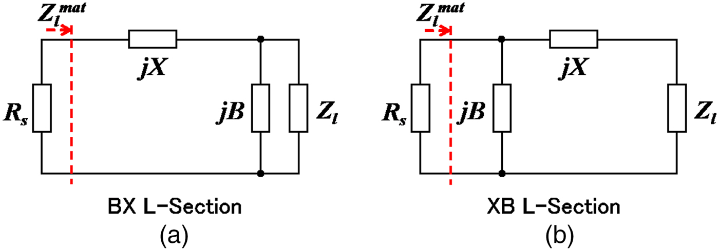
is the synthesized impedance at the target side of the matching circuit as shown in Fig. 1. L-section matching circuit with one shunt component and one series component has two available topologies as shown in Fig. 1, they are BX topology and XB topology, respectively. In this paper, the susceptance B designates a shunt component and reactance X is used as a series component. Positive B and negative X mean the components are capacitors, and others are inductors.
L-section matching circuit.

The selecting conditions for the topologies can be represented by the relationship between the impedances of Z l and Z s , and also the relationship between the admittances of Y l = 1/Z l = G l + jB l and Y s = 1/Z s = G s . They are expressed in the following,
 $$BX\;{\rm type}\;{\rm is}\;{\rm selected}\;{\rm when}\;G_l \lt G_s$$
 $$XB\;{\rm type}\;{\rm is}\;{\rm selected}\;{\rm when}\;R_l \lt R_s$$
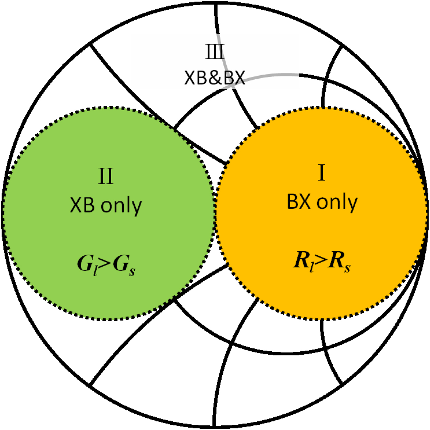
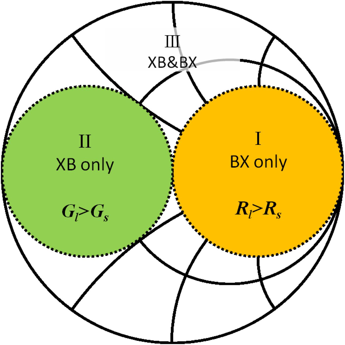
As shown in Fig. 2, Smith Chart is divided into three areas according to the magnitude relationship between G l and G s , or R l and R s . When G l <G s , the load admittance is located in the area I and area III, when R l <R s , the load impedance is located in the area II and area III in Smith Chart, respectively. The two dotted circles which denote R l = R s and G l = G s , respectively, are the boundaries to determine the topologies of matching circuits. BX L-section can be only effective when the load impedance is located in area I, while XB L-section can be only useful when the load impedance is located in area II. However, both BX and XB type matching circuits can be applied to these load impedances which are located inside of area III.
L-section topology depending on Z s and Z l position in Smith chart.
In case of G l <G s , BX type is selected. The susceptance B and reactance X are deduced by the matching condition exactly as
 $$B = - B_l \pm \sqrt {G_lG_s - G_l^2}, $$
 $$X = \pm \displaystyle{{\sqrt {G_lG_s - G_l^2}} \over {G_lG_s}}.$$
In the same way, for the case of R l < R s , XB type is selected. B and X can be deduced as
 $$X = - X_l \pm \sqrt {R_lR_s - R_l^2}, $$
 $$B = \pm \displaystyle{{\sqrt {R_lR_s - R_l^2}} \over {R_lR_s}}.$$
Equations (1), (3) and (2), (4) are compatible because if B, X, G are replaced by corresponding X, B, R, equations (1) and (2) will be equations (3) and (4). This compatibility makes the program code to obtain any L-section matching circuit very easy to implement.
III. PROPOSED EXACT DESIGN APPROACH OF LOSSY L-SECTION MATCHING CIRCUIT
In the practical case, inductors and capacitors have intrinsic ohmic loss in addition to their reactive components. Here, an exact approach to design a L-section matching circuit with ohmic loss is presented. Let Q-factors Q B and Q X represent the ohmic losses in B and X, respectively, those are
 $$Q_B = \vert B \vert /G, \Rightarrow G = \vert B \vert /Q_B$$
 $$Q_X = \vert X \vert /R, \Rightarrow R = \vert X \vert /Q_X$$
where R represents the ohmic loss of X, while G represents the ohmic loss of B, respectively.
For the case of G l < G s , BX L-section matching is selected. From the matching condition, the following equations with unknowns B and X are established,
 $$\displaystyle{{ \vert X \vert} \over {Q_X}} + \displaystyle{{G_l + \vert B \vert /Q_B} \over {{(G_l + \vert B \vert /Q_B)}^2 + {(B_l + B)}^2}} = R_s,$$
 $$X = \displaystyle{{B_l + B} \over {{(G_l + \vert B \vert /Q_B)}^2 + {(B_l + B)}^2}}.$$
Usually, Q X and Q B can be estimated from the datasheets of the products, thus, B and X can be obtained exactly by solving equations (7) and (8).
Similarly, in case of R l < R s , XB L-type is selected, the following equations with unknowns B and X are obtained from the matching condition,
 $$\displaystyle{{ \vert B \vert} \over {Q_B}} + \displaystyle{{R_l + \vert X \vert /Q_X} \over {{(R_l + \vert X \vert /Q_X)}^2 + {(X_l + X)}^2}} = G_s,$$
 $$B = \displaystyle{{X_l + X} \over {{(R_l + \vert X \vert /Q_X)}^2 + {(X_l + X)}^2}},$$
again, both B and X can be obtained exactly by solving equations (9) and (10).
IV. FEATURES OF LOSSY L-SECTION MATCHING CIRCUIT
This section investigates the differences between CMA and PMA. Subsection (A) focuses on selecting boundaries of the matching circuit topologies for different impedances. Subsection (B) focuses on the synthesized impedances
 $Z_l^{mat} $
and
 $Z_s^{mat} $
at two sides of the matching circuit.
A) Boundaries of selecting condition for matching circuit topology
Without the ohmic loss of a reactive component, the circles
 $\overline {R_l} = (R_l/R_s) = 1$
and
 $\overline {G_l} = (G_l/G_s) = 1$
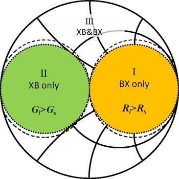
in Smith Chart are the boundaries of area I, area II, and area III. They are shown in Fig. 3 as dotted lines. Without ohmic loss, only BX topology can be selected as the matching circuit for the load impedances in area I while only XB topology can be applied to area II, and both BX and XB topologies are capable of being used as the matching circuits in area III. However, if the reactive components used in the matching circuit have some ohmic losses, the boundaries of area I and area II are changed from dotted lines to the dashed lines as shown in Fig. 3. The shape and location of dashed lines depend on the Q
X
in case of BX L-section, and Q
B
in case of XB L-section. It is because from equation (7), R
s
seems to be decreased by |X|/Q
X
if |X|/Q
X
is moved from the left side to the right side of equation (7), and similarly, from equation (9) G
s
seems to be decreased by |B|/Q
B
if |B|/Q
B
is moved from the left side to the right side of equation (9). The two dashed lines will be moved outside from the
 $\overline {R_l} = (R_l/R_s) = 1$
and
 $\overline {G_l} = (G_l/G_s) = 1$
when Q
X
in BX L-section and Q
B
in case of XB L-section become small. Small Q
X
and Q
B
mean the losses of the reactive components are large. The dashed line will return to the circles
 $\overline {R_l} = (R_l/R_s) = 1$
or
 $\overline {G_l} = (G_l/G_s) = 1$
when Q
X
in BX L-section and Q
B
in case of XB L-section get large enough. The change of boundary conditions with ohmic losses of reactive components means the impedance located in area III will be inside area I or area II which will happen for the small dipoles and the coils coupling WPT scenarios as used as the practical examples in next section.
Boundaries of CMA and PMA to select topologies of the matching circuit in Smith Chart.

B) Synthesized impedances
 $Z_l^{mat} $
and
$Z_s^{mat} $
at two sides of the matching circuit


When a load impedance Z
l
is matched to target impedance of Z
s
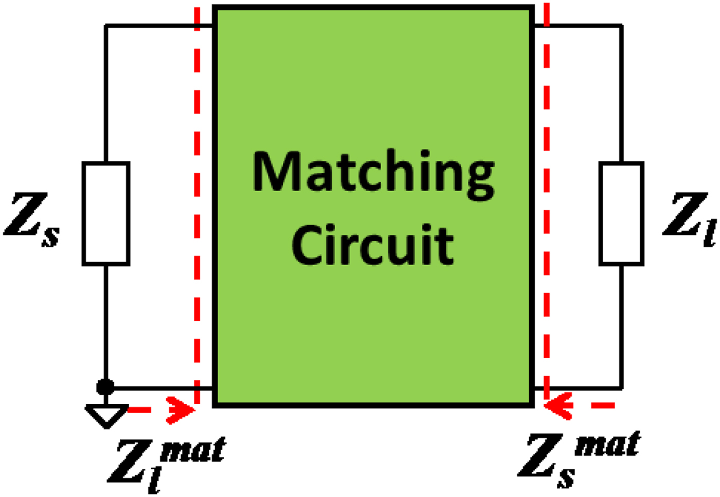
by using lossless matching circuit as shown in Fig. 4, the synthesized impedance
 $Z_l^{mat} $
at the target impedance side of matching circuit, otherwise looking into the matching circuit and Z
l
, is certainly satisfied with the matching condition, which is
 $$Z_l^{mat} = Z_s^*. $$
Synthesized impedances
 $Z_l^{mat} $
and
 $Z_s^{mat} $
at two sides of the matching circuit.
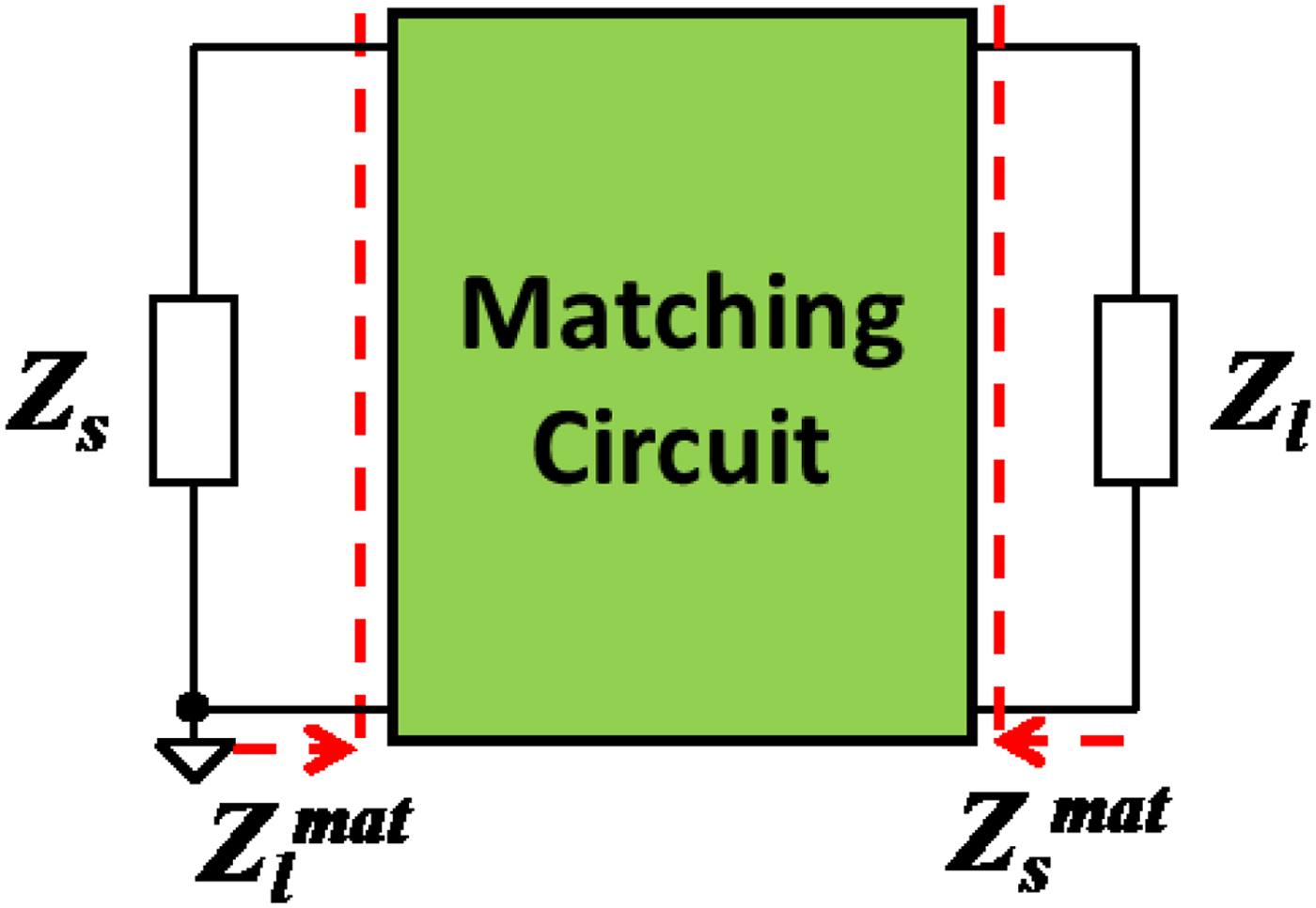
And also the synthesized impedance
 $Z_s^{mat} $
looking into the matching circuit and Z
s
is satisfied with the matching condition, that is,
 $$Z_l^* = Z_s^{mat}. $$
That means the matching circuit without ohmic loss can meet the matching conditions at both sides of the matching circuit simultaneously. However, this situation is changed when the matching circuit has the ohmic loss in its reactive components. If the B and X are obtained from the matching condition of
 $Z_l^{mat} = Z_s^* $
by our proposed method, the matching condition at other side
 $Z_l^* = Z_s^{mat} $
is not guaranteed again or vice versa due to the loss of matching circuit.
V. EXAMPLES
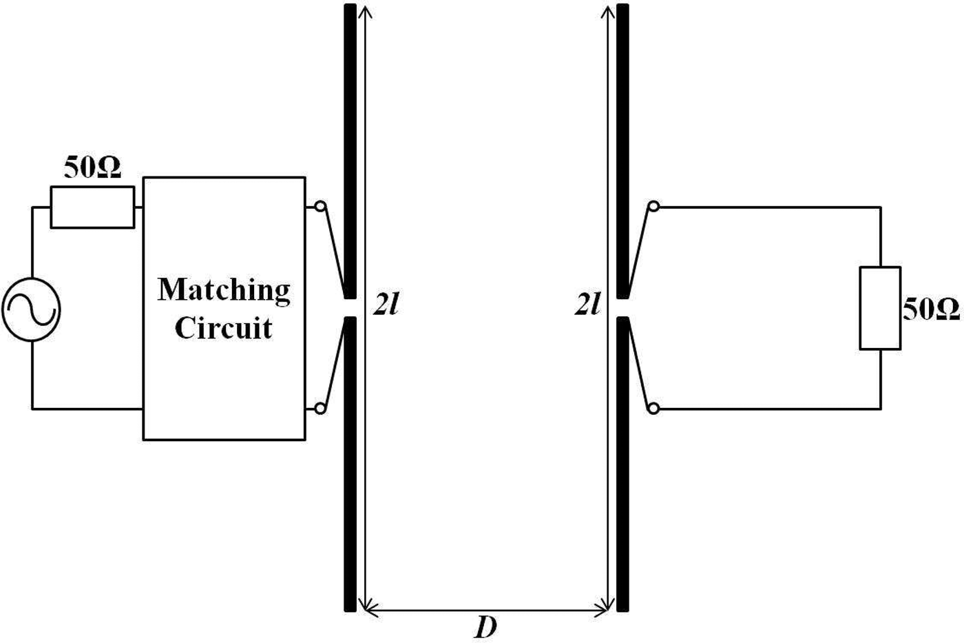
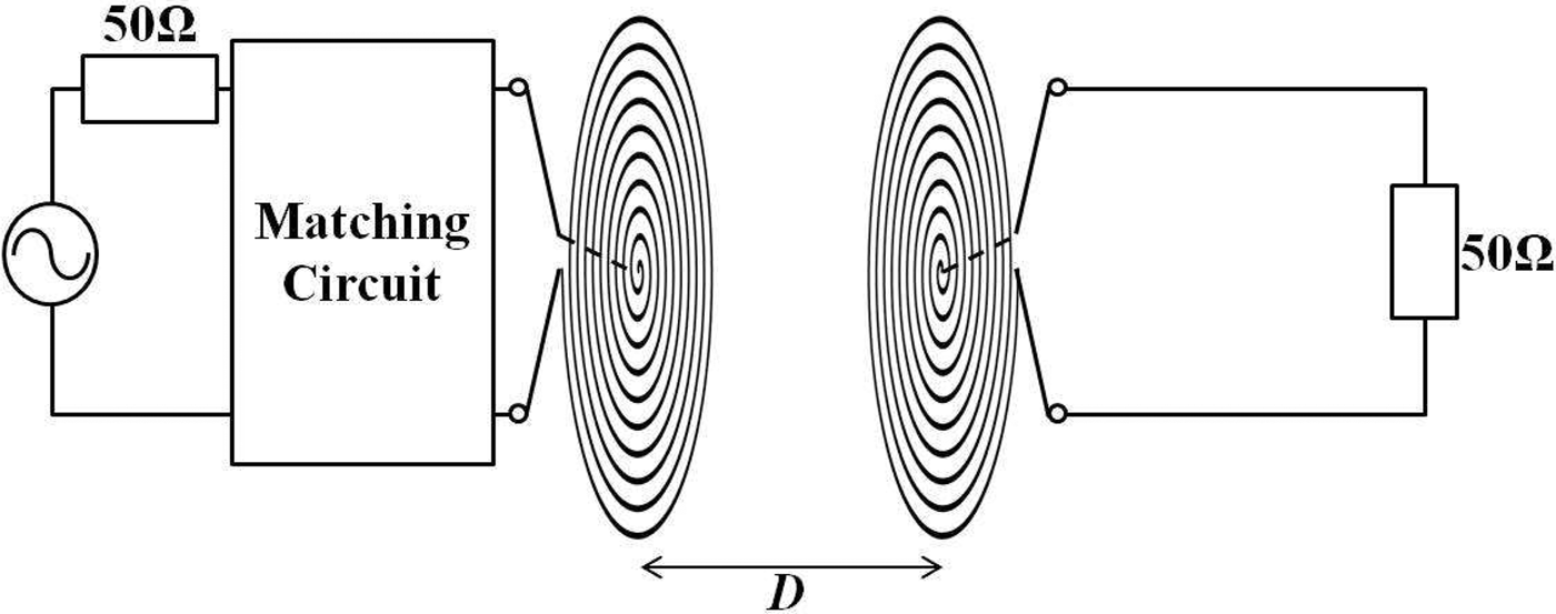
This section shows the simulation results of four different kinds of load impedances. The target impedance is set to 50 Ω, and the load impedances are 100 + j50 Ω, 1 + j6 Ω, 4.47 − j1166 Ω, and 2.90 + j1686 Ω, respectively. Especially, 4.47 − j1166 Ω is the impedance of electrically small transmitting dipole antenna of 2l = 0.1λ as used in WPT transmission model in Fig. 5, where the receiving antenna has the same dipole antenna structure loaded by 50 Ω. 2.90 + j1686 Ω is the input impedance of 20 turns coil as used in WPT transmission model in Fig. 6, where the receiving antenna has the same coil structure loaded by 50 Ω. The distances D in both dipoles and coils WPT systems are 0.1 wavelengths. Both impedances at transmitting side include the mutual coupling from the receiving elements.
An example of WPT system using small dipole antennas.

An example of WPT system using 20 turns coils.

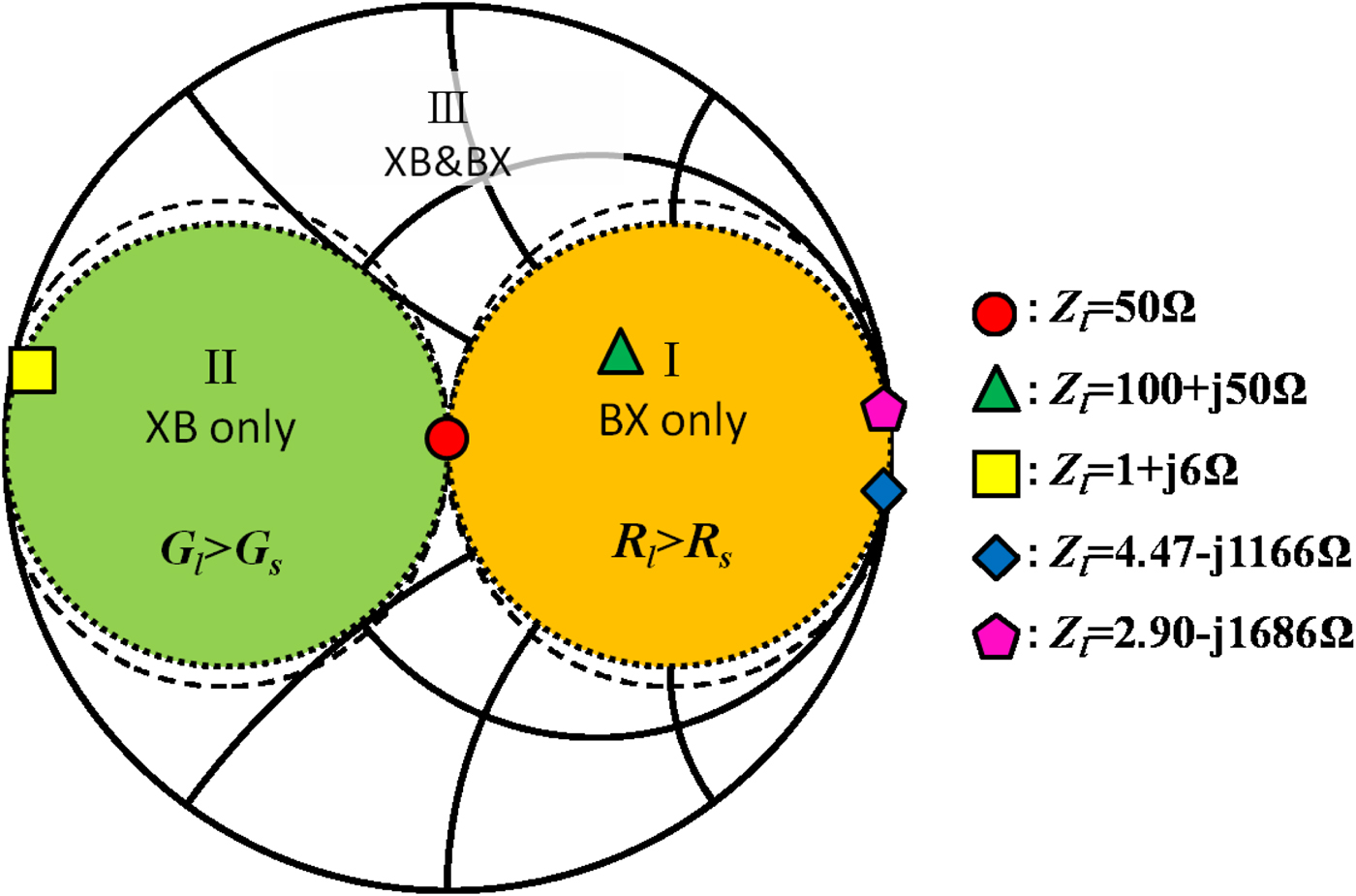
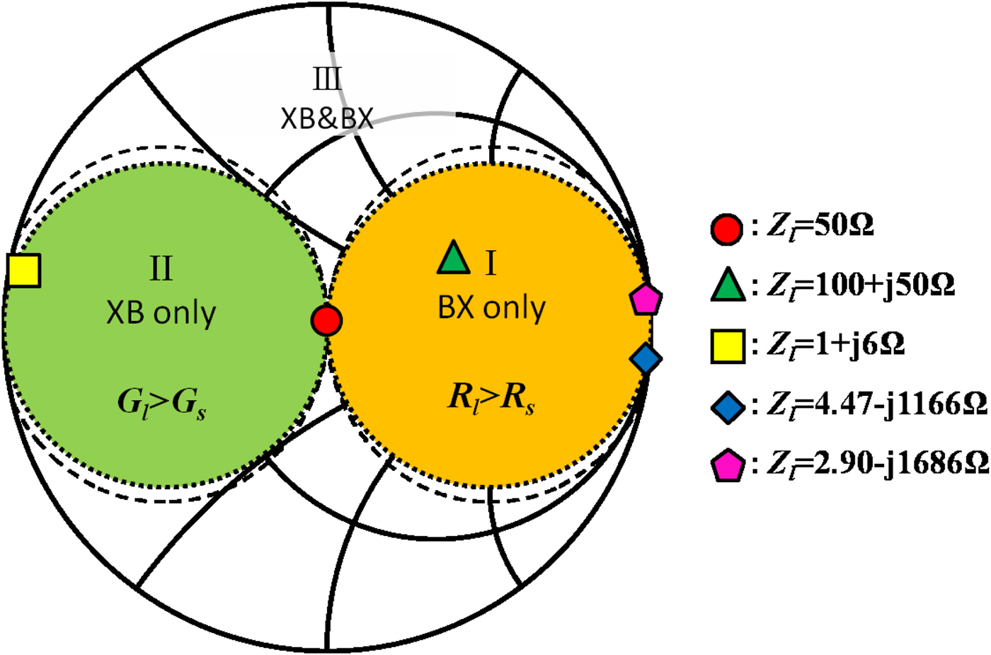
Fig. 7 shows the positions of four kinds of load impedances on the Smith chart. 100 + j50 Ω is located in area I, 1 + j6 Ω is located in area II, 4.47 − j1166 Ω and 2.90 + j1686 Ω are located in area III if the ideal matching circuits without ohmic losses are applied. Four kinds of impedances represent the impedances in three areas, that is why we use them as the example load impedances. The impedance of WPT system where two dipoles are used has a very small resistance and a large negative reactance and is located in area III, while that of two coils has very small resistance and large positive reactance and also located in area III. Therefore, the matching design methods for dipoles and coils coupling will be very similar.
The positions of load impedances in Smith Chart.
A) Lossless matching circuit design
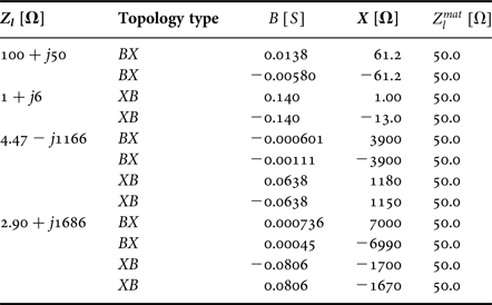
Firstly, the CMA using ideally reactive components without the ohmic loss is used to design the matching circuits for the above four kinds of load impedances. The reactive components X and B of each matching circuit calculated by CMA are listed in Table 1. When Z
l
= 100 + j50 Ω, BX L-section matching circuit is used due to G
l
< G
s
. When Z
l
= 1 + j6 Ω, satisfying R
l
< R
s
, then XB L-section matching circuit is used. Both BX and XB L-section matching circuits are used as the matching circuits when Z
l
= 4.47 − j1166 Ω and Z
l
= 2.90 + j1686 Ω, because Z
l
= 4.47 − j1166 Ω and Z
l
= 2.90 + j1686 Ω are in area III of the Smith Chart as shown in Fig. 2. The synthesized impedances
 $Z_l^{mat} $
are equivalent to target impedance of 50 Ω, and it represents that all matching circuits can get matched to the target impedance 50 Ω by CMA.
Components of the L-section matching circuit without loss.

As shown in Table 1, it can be observed that there are two selective values for B and X even with the same L-section topology BX or XB because equations (1)–(4) for B and X have both plus and minus solutions. For example, when Z
l
= 100 + j50 Ω, BX L-section matching circuit is applied, there are still two solutions for the elements. One solution uses Shunt C and series L as matching components with
 $B = 0.138{\kern 1pt} S{\kern 1pt}, X = 61.2\;\Omega $
, and the other uses shunt L and series C as matching components with
 $B =- 0.0058{\kern 1pt} S{\kern 1pt},X = - 61.2\;\Omega $
. In later part of this paper, the symbols BX-CL and BX-LC will be used for denoting the above two kinds of matching circuit.
B) Lossy matching circuit design
Here, the reactive components used in matching circuit will be treated as the practical ones, meaning the ohmic losses will be taken into account. Both CMA and PMA will be applied to design the L-section matching circuits. Certainly, the values of reactive components are calculated ignoring the ohmic loss when CMA is used.
The synthesized impedances
 $Z_l^{mat} = R_l^{mat} + jX_l^{mat} $
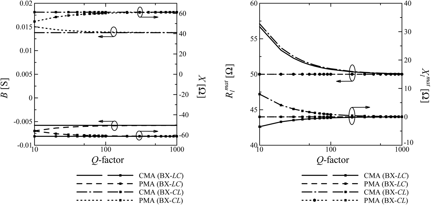
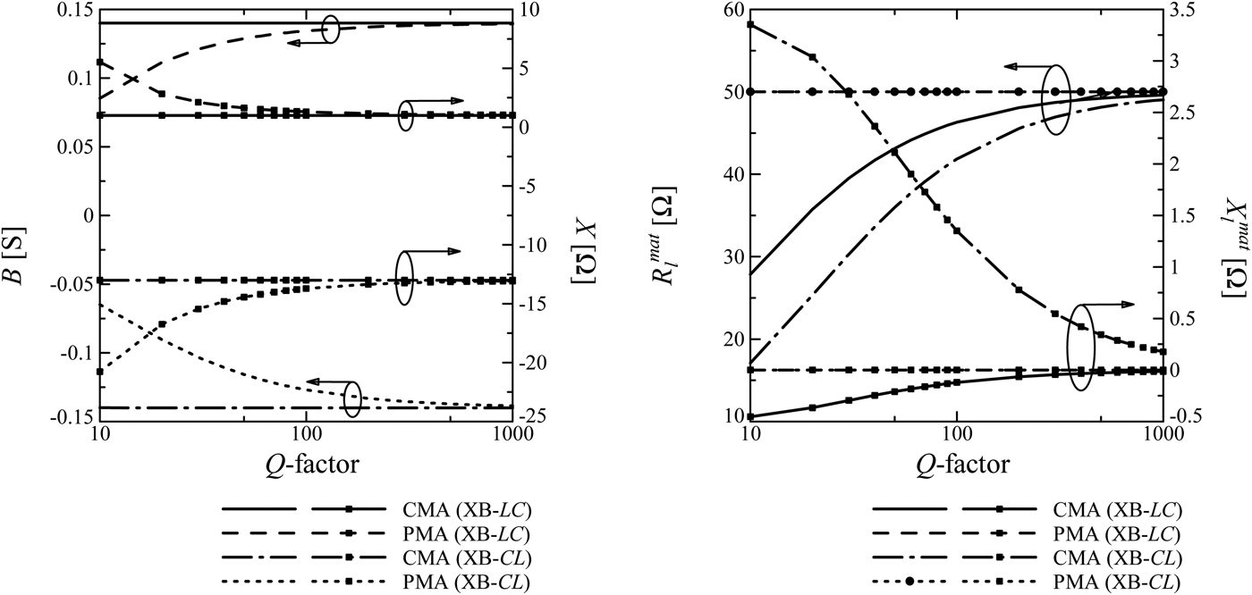
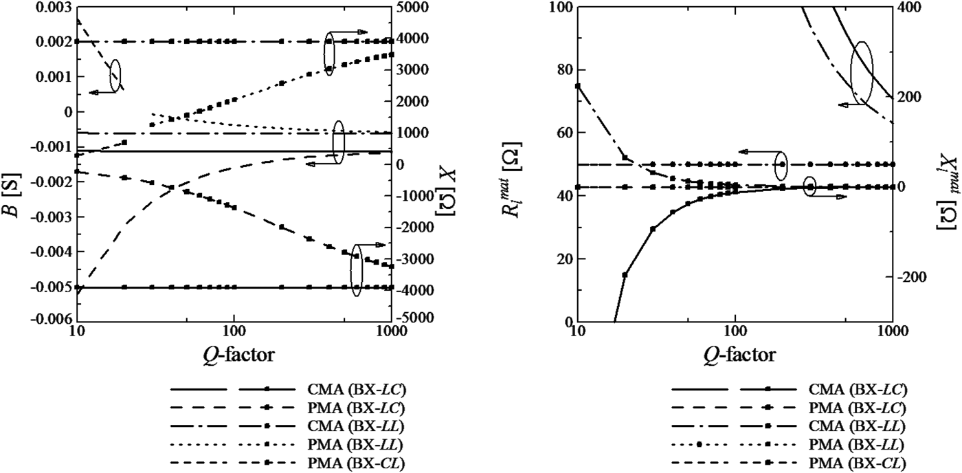
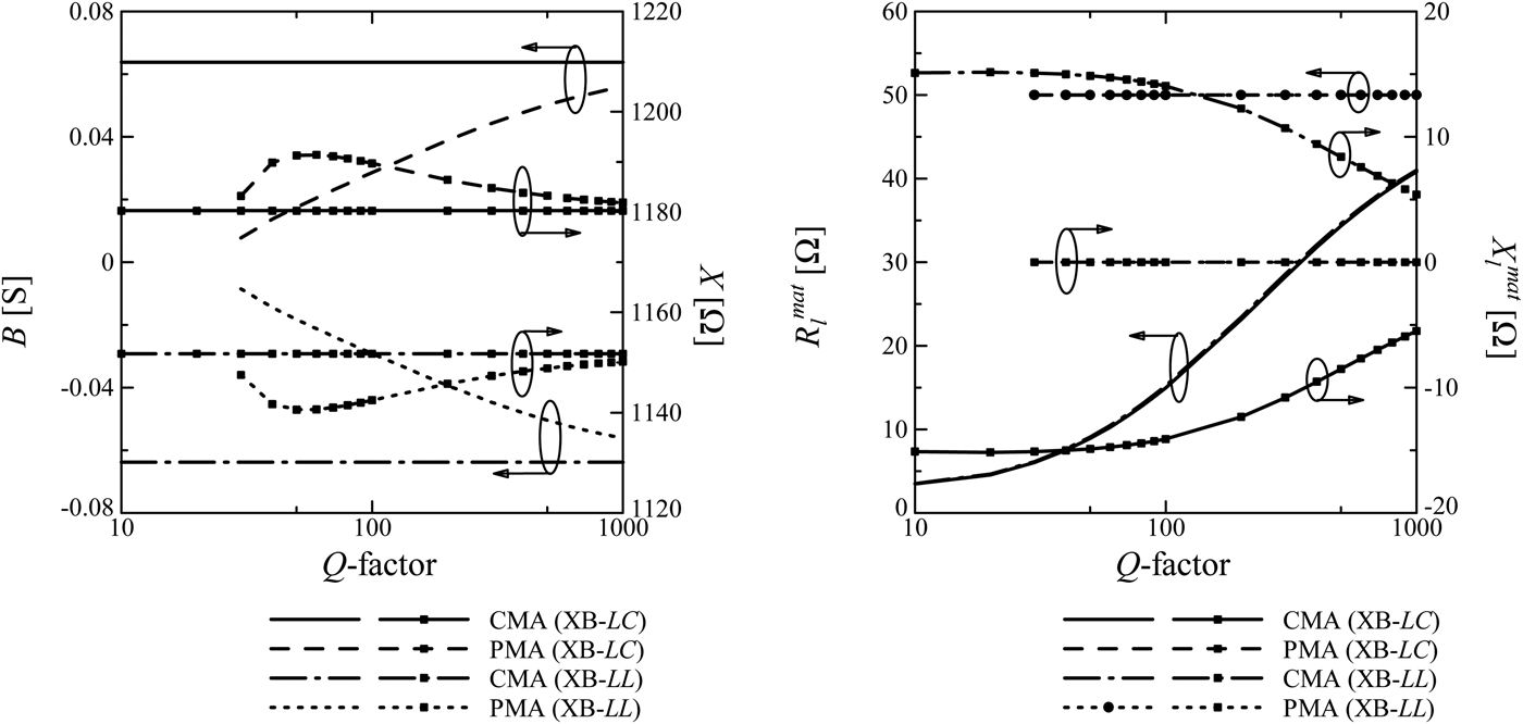
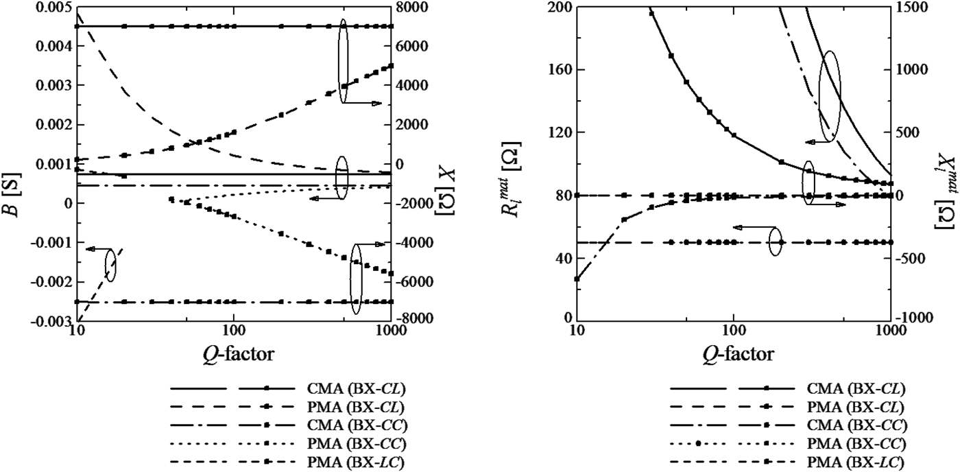
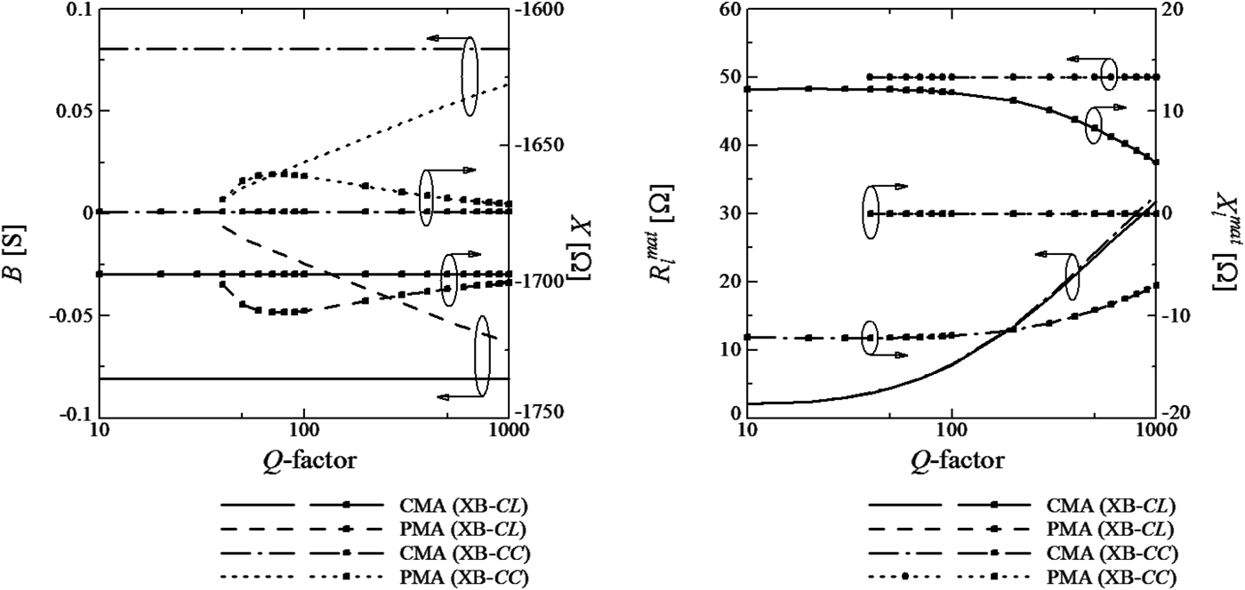
versus the Q factors by using the CMA and the PMA are compared in Figs 8–13, where Q
X
= Q
B
. Figure 8 is for Z
l
= 100 + j50 Ω, Fig. 9 is for Z
l
= 1 + j6 Ω, Figs 10 and 11 are for Z
l
= 4.47 − j1166 Ω, and Figs 12 and 13 are for Z
l
= 2.90 + j1686 Ω. As seen,
 $Z_l^{mat} $
obtained by using the CMA does not equal to R
s
except the case when Q-factor is larger than about 500, but all
 $Z_l^{mat} $
obtained by using the PMA are equivalent to target impedance R
s
for any Q-factor. Therefore, it is validated that the PMA is an effective approach to design a matching circuit when the ohmic loss is considered. And it is also seen that the values of both reactance and susceptance obtained by PMA are approaching to the values obtained by CMA when both Q-factors are large enough. In Fig. 11, the XB topology can be only used when Q ≥ 30. Because 4.47 − j1166 Ω is located in area I when Q < 30, XB topology cannot be applied in this case. It makes that there are three types of BX topologies obtained by PMA in Fig. 10 for 4.47 − j1166 Ω due to the same reason. Similarly, it happens on coil types as shown in Figs 12 and 13.
B, X and
 $Z_l^{mat} $
versus Q-factor (Z
l
= 100 + j50 Ω, BX Topology).

B, X and
 $Z_l^{mat} $
versus Q-factor (Z
l
= 1 + j6 Ω, XB Topology).

B, X and
 $Z_l^{mat} $
versus Q-factor (Z
l
= 4.47 − j1166 Ω, BX Topology).

B, X and
 $Z_l^{mat} $
versus Q-factor (Z
l
= 4.47 − j1166 Ω, XB Topology).

B, X and
 $Z_l^{mat} $
versus Q-factor (Z
l
= 2.90 + j1686 Ω, BX Topology).

B, X and
 $Z_l^{mat} $
versus Q-factor (Z
l
= 2.90 + j1686 Ω, XB Topology).

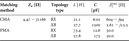
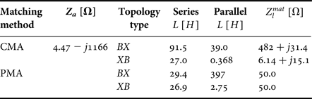
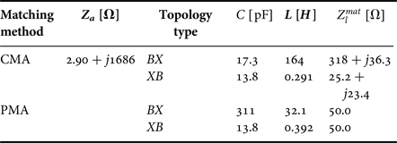
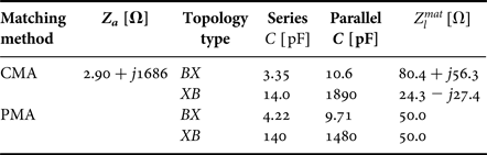
Tables 2 and 3 show the values of inductor and capacitor of the matching circuits to 4.47 − j1166 Ω where two electrically small dipoles are used as shown in Fig. 5. Table 2 shows four types of matching circuits consisting of one inductor and one capacitor, and Table 3 shows four types of matching circuits consisting of two inductors. Tables 4 and 5 show the values of inductor and capacitor of the matching circuits to 2.90 + j1686 Ω where the 20 turns helical coils are used as shown in Fig. 6. Table 4 shows four types of matching circuits consisting of one inductor and one capacitor, and Table 5 shows four types of matching circuits consisting of two capacitors. For Tables 2–5, the frequency is set to be 6.78 MHz. And from practical datasheets of chip elements, Q-factors of inductor and capacitor are set to be 30 and 1000, respectively.
Impedance matching circuits consisting of inductor and capacitor for dipole antenna.

Impedance matching circuits consisting of two inductors for dipole antenna.

Impedance matching circuits consisting of capacitor and inductor for 20 turns coil.

Impedance matching circuits consisting of two capacitors for 20 turns coil.

From the above tables, it has been demonstrated that CMA cannot design the correct matching circuit to meet the matching condition for electrically small dipole antenna and coils coupling WPT system. However, PMA can design the correct matching circuit.
C) Transmission efficiencies versus reactive component Q-factors of L-section matching circuit
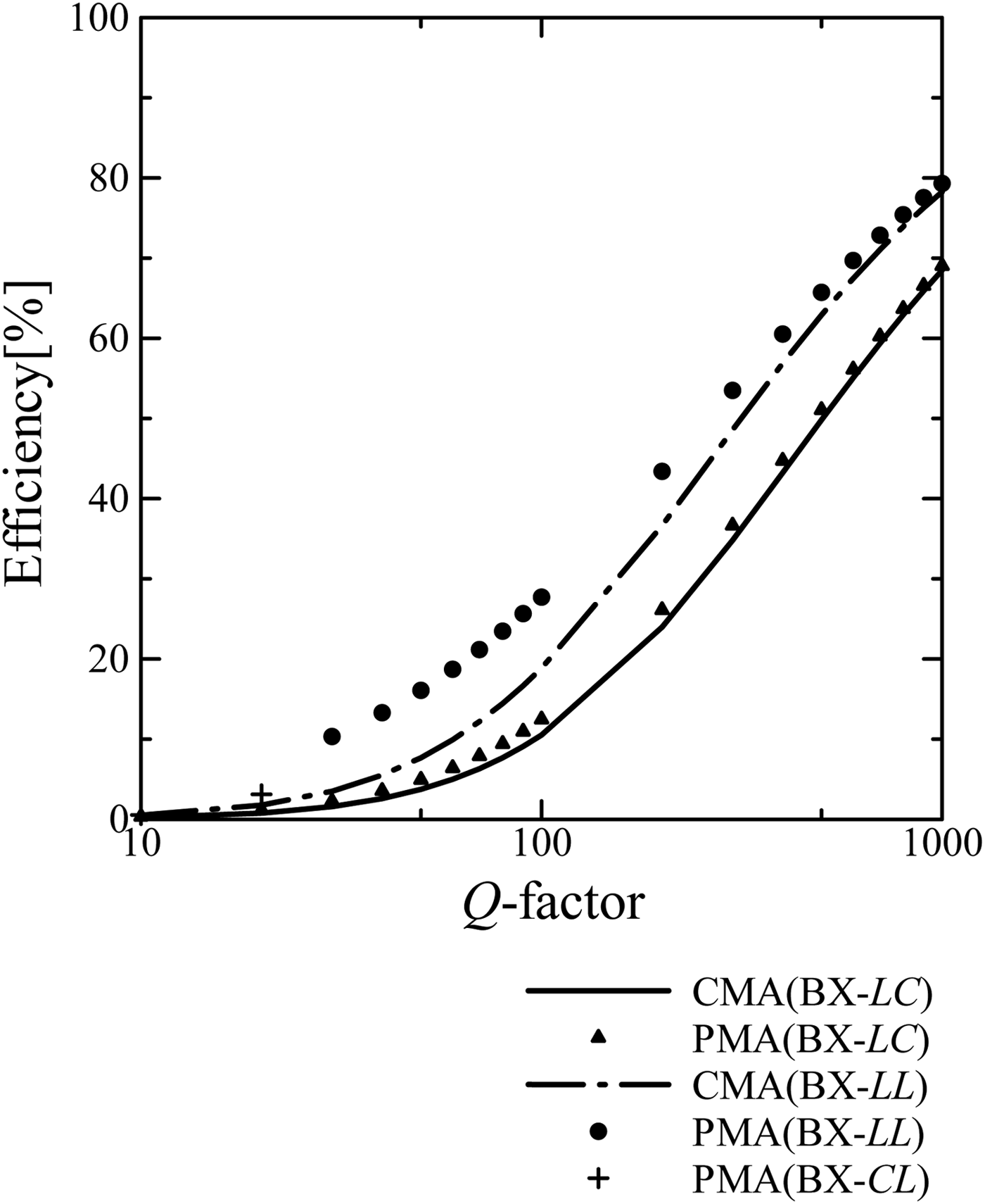
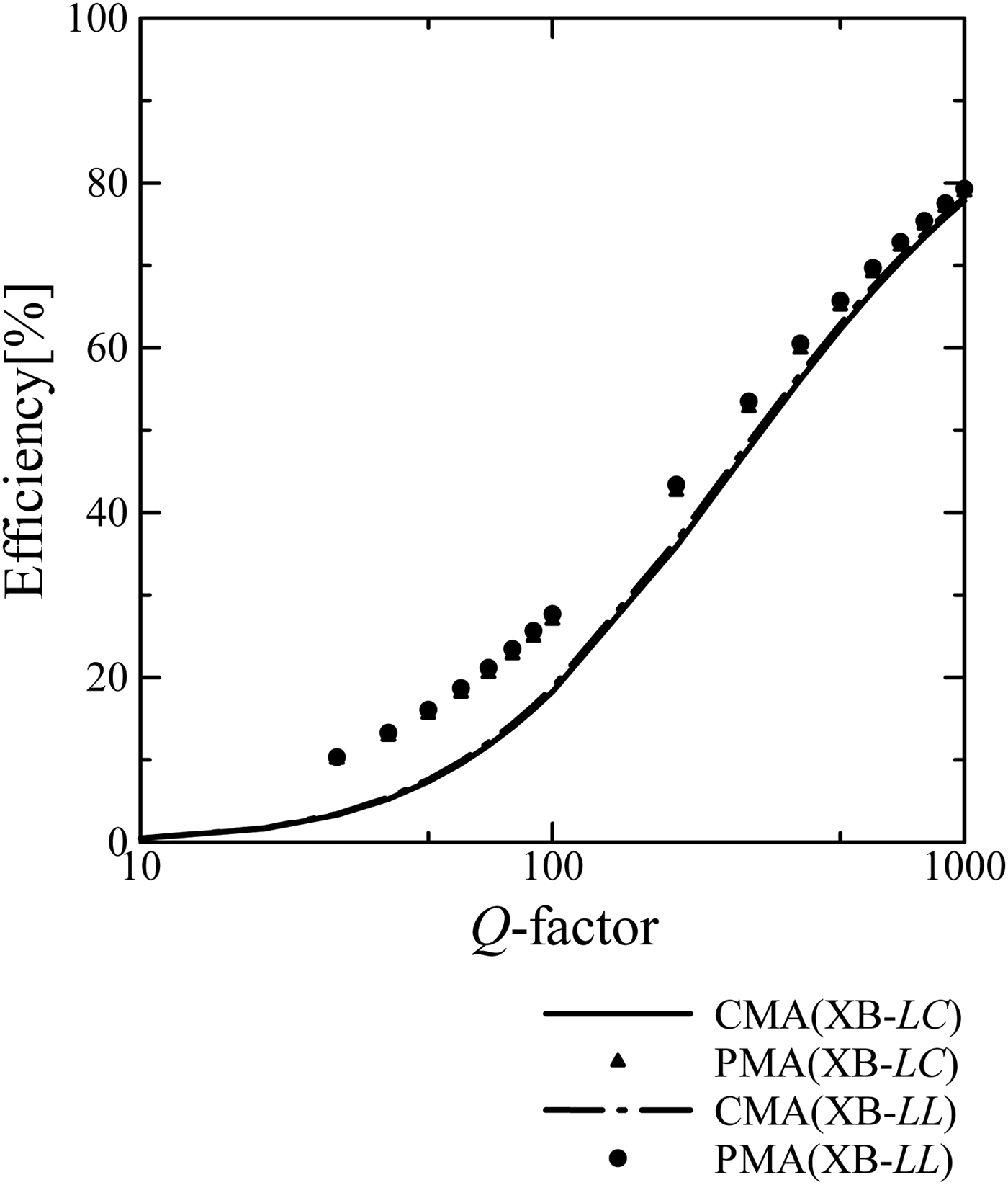
Furthermore, the transmission efficiencies versus Q-factor with L-section matching circuit for Z l = 100 + j50 Ω and 1 + j6 Ω are plotted in Figs 14 and 15. The efficiency in this paper is defined as P l /P a , where P l denotes the power consumed at Z l and P a is the available maximum power input into the matching circuit. In [Reference Yuan, Chen and Sawaya3, Reference Chen, Ozawa, Yuan and Sawaya4, Reference Chen and Yuan18], the optimal impedances at both sides for maximum transfer efficiency were deduced and included in the mutual coupling effect between the transmitting and receiving sides. The main purpose of this paper is how to realize these two optimal impedances at both transmitting and receiving sides, which is how to design matching circuit between two arbitrary impedances. So the efficiency discussed in this paper is limited to the power delivery between two impedances, not between the transmitting and receiving elements. The efficiency defined in [Reference Yuan, Chen and Sawaya3, Reference Chen, Ozawa, Yuan and Sawaya4, Reference Chen and Yuan18] is equivalent to the transducer power gain as defined in [Reference Rahola5, Reference Collin20]. For the case of Z l = 100 + j50 Ω, two types of BX L-sections as shown in Fig. 14 are available as the matching circuits. The efficiencies of shunt L and series C are better than shunt C and series L for both lossless and lossy design approaches. For the case of Z l = 1 + j6 Ω, two types of XB L-sections as shown in Fig. 15 are available as the matching circuits. The efficiencies of series L and shunt C matching circuit are better than those of series C and shunt L circuit for both CMA and PMA. The efficiencies with PMA are less than those with CMA.
Efficiency versus Q-factor (Z l = 100 + j50 Ω, BX Topology).

Efficiency versus Q-factor (Z l = 1 + j6 Ω, XB Topology).

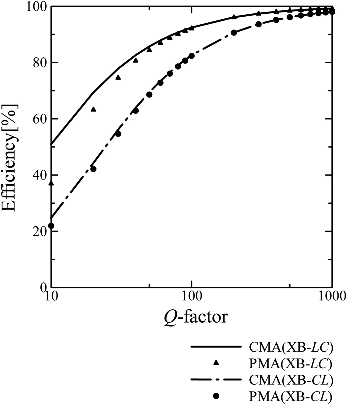
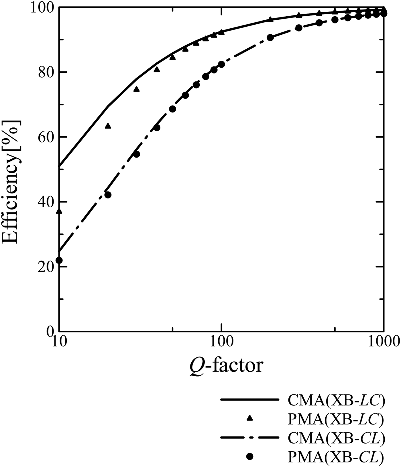
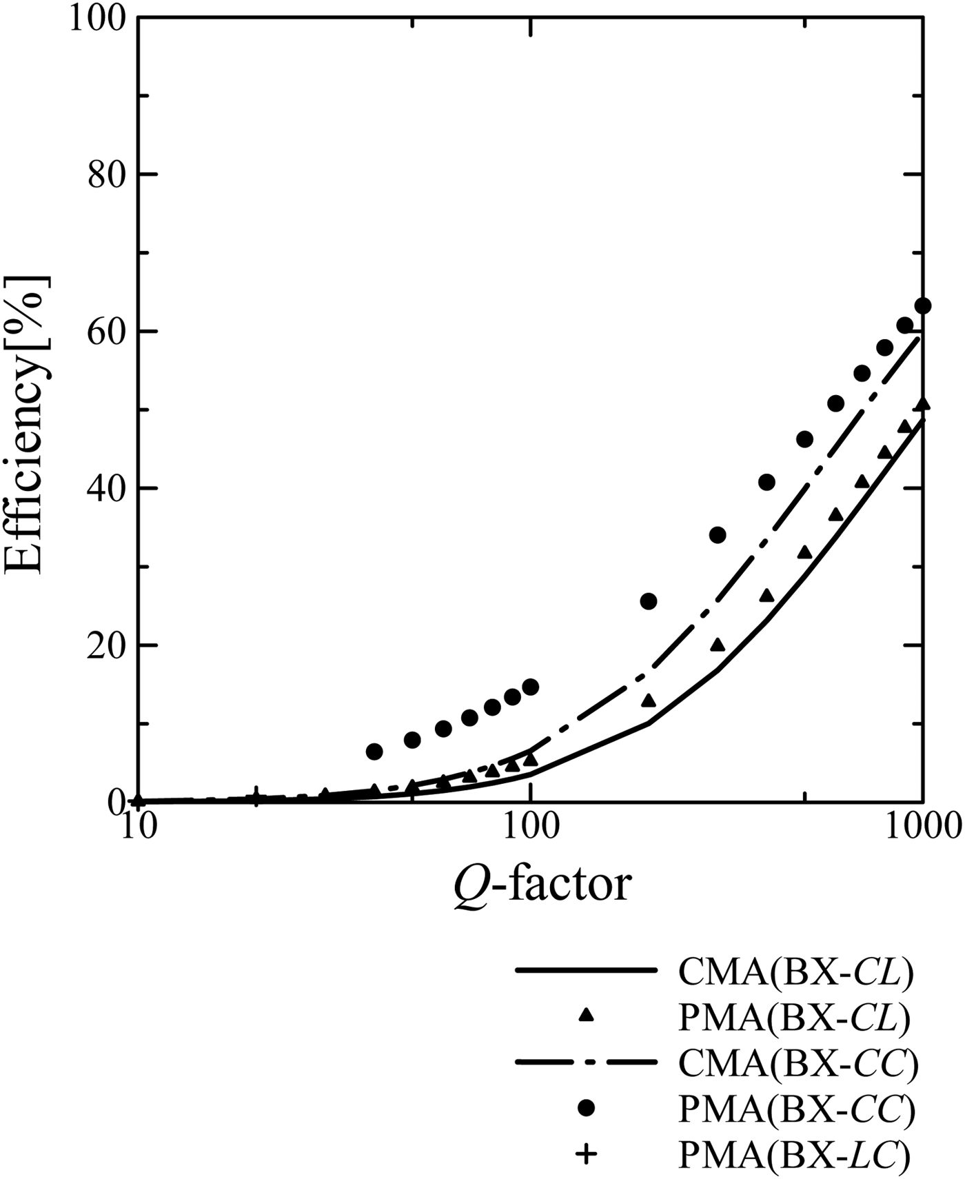
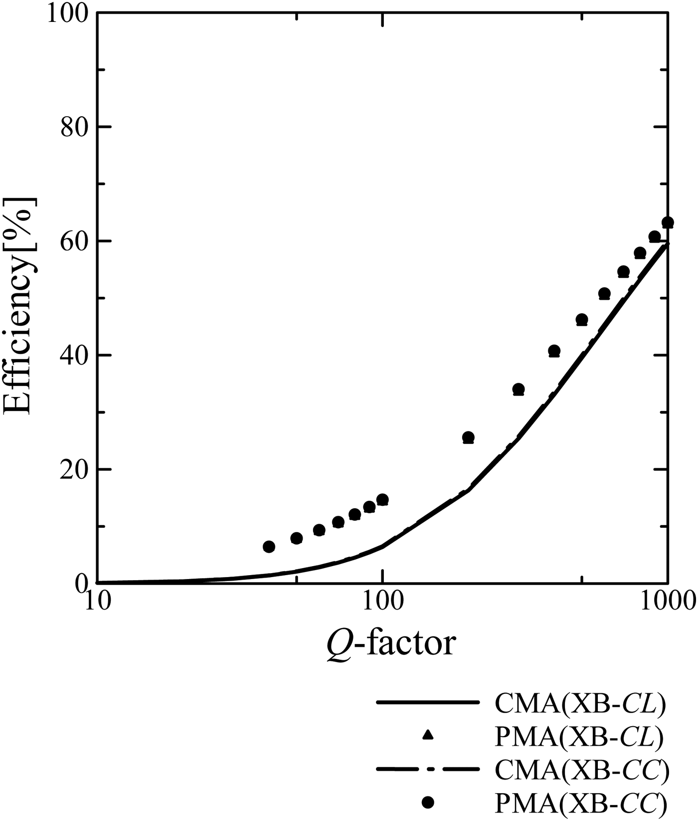
For the case of 4.47 − j1166 Ω, three types of BX L-sections and two types of XB L-sections are available as the matching circuits in PMA. In the BX topology, the efficiencies of shunt L and series L circuit are better than those of shunt L and series C circuit. At Q X = Q B = 30, shunt L and series L circuit is replaced by shunt C and series L circuit due to the changing of the relationship between Z l and Z s in PMA. In the XB topology, the efficiencies of series L and shunt L are better than those of series L and shunt C circuit for both methods, designed either by CMA or PMA. For the case of 2.90 + j1686 Ω, three types of BX L-sections and two types of XB L-sections are available as the matching circuits in PMA. In the BX topology, the efficiencies of shunt C and series C circuit are better than those of shunt C and series L circuit. At Q X = Q B = 40, shunt C and series C circuit is replaced by shunt L and series C circuit due to the changing of the relationship between Z l and Z s in PMA. In the XB topology, the efficiencies of series C and shunt C are better than those of series C and shunt L circuit for both methods, designed either by CMA or PMA. Different from the cases when Z l = 100 + j50 Ω and Z l = 1 + j6 Ω, the efficiencies by using the PMA is higher than those by using the CMA.
Comparing with CMA, the efficiency reduction by PMA for the cases of Z l = 100 + j50 Ω and Z l = 1 + j6 Ω results from the requirement of the larger B or X which brings with the larger ohmic loss. However, the PMA does improve the total deficiency for the practical cases when load impedance are 4.47 − j1166 Ω and 2.90 + j1686 Ω. For the matching circuit without ohmic loss, the efficiency between two arbitrary impedances will be the maximum one according to conjugate matching condition, and it gives the higher efficiency obtained by PMA when ohmic loss is taken into account for the impedance with very small resistance and large reactance. However, the efficiency between two arbitrary impedances by PMA is not the highest one. How to obtain the highest one for the efficiency between two arbitrary impedances and also WPT system at the presence of the ohmic loss in the matching circuit will be our next research topics (Figs 16–19).
Efficiency versus Q-factor (Z l = 4.47 − j1166 Ω, BX Topology).

Efficiency versus Q-factor (Z l = 4.47 − j1166 Ω, XB Topology).

Efficiency versus Q-factor (Z l = 2.90 + j1686 Ω, BX Topology).

Efficiency versus Q-factor (Z l = 2.90 + j1686 Ω, XB Topology).

VI. CONCLUSIONS
An exact method to design L-section lumped impedance matching circuit with elements’ ohmic losses has been proposed in this paper. It has been confirmed that the proposed method is effective for any two different impedances to satisfy the complex conjugate matching condition. The effects of ohmic loss and mismatching on the matching circuit efficiency have been investigated by some examples including two practical models when two electrically small dipole antennas and two coils are used as transmitting and receiving elements in WPT system. And it has been found that the improvement on the efficiency by using the proposed exact matching circuit approach is achieved when the impedance has very low resistance and the large reactive part which usually happens on an electrically small dipole or coils. Additionally, in this paper, the following novel results have been obtained.
-
(1) The perfect selection topology conditions have been established and very easy to be applied to any cases when ohmic losses do not exist. And the modification of the conditions for lossy matching circuit has been also proposed.
-
(2) It has been confirmed that the matching condition is satisfied at only one side of the matching circuit when the impedance matching circuit has ohmic losses. Therefore, the complex conjugate matching condition does not guarantee to achieve the maximum transmission efficiency of the matching circuit if the losses of lumped elements are considered.
ACKNOWLEDGEMENTS
This work was partly supported by JSPS KAKENHI Grant Number 25420394 and SCOPE No.16769614.
 Satoshi Suzuki received the Bachelor of Engineering from National Institute of Technology, Sendai College in 2017. He is pursuing the Master’s degree in Engineering at Tohoku University. His main research interests are optimization of impedance matching circuit and design of schottky barrier diode for energy harvesting.
 Qiaowei Yuan received the B.E., M.E., and Ph.D. degrees from Xidian University, Xi'an, China, in 1986, 1989, and 1997, respectively. From 1992 to 1995, she worked in Sendai Research and Development Laboratory, Matsushita Communication Company, Ltd.; from 1997 to 2007, with Sendai Research and Development Center, Oi Electric Company Ltd. and with Intelligent Cosmos Research Institute, Japan. From 2007 to 2008, she was an Associate Professor of Tokyo University of Agriculture and Technology. She is currently a Professor of National Institute of Technology, Sendai College. Dr. Yuan received the Best Paper Award and Zenichi Kiyasu Award in 2009 from the Institute of Electronics, Information and Communication Engineers (IEICE) of Japan. Dr. Yuan severed as the secretary of IEICE Technical Committee on Wireless Power transfer of Japan from 2013 to 2015; and she also was a visiting scholar at ElectroScience Laboratory of Ohio State University in USA from April 2015 to September 2015.
 Qiang Chen received the B.E. degree from Xidian University, Xi’an, China, in 1986, the M.E. and D.E. degrees from Tohoku University, Sendai, Japan, in 1991 and 1994, respectively. He is currently Chair Professor of Electromagnetic Engineering Laboratory with the Department of Communications Engineering, Faculty of Engineering, Tohoku University. Dr. Chen received the Young Scientists Award in 1993, the Best Paper Award and Zen-ichi Kiyasu Award in 2009 from IEICE. He was the Secretary and Treasurer of IEEE AP Society Tokyo Chapter in 1998, the Secretary of Technical Committee on EMCJ of IEICE from 2004 to 2006, the Secretary of Technical Committee on AP of IEICE from 2008 to 2010, and an Associate Editor of IEICE Transactions on Communications from 2007 to 2012. He served as Chair of IEICE Technical Committee on PEM from 2012 to 2014. He is now Chair of IEICE Technical Committee on WPT, and Chair of IEEE AP Society Japan Chapter.