I. INTRODUCTION
Tin dioxide (SnO2), Reference Zheng, Jang and Yao1–Reference Van Quang, Van Dung, Trong, Hoa, Van Duy and Hieu4 as a typical metal oxide semiconductor like zinc oxide (ZnO), Reference Prades, Cirera and Morante5–Reference Ahn, Park, Heo, Park, Kim and Choi11 was widely applied as excellent gas sensing materials in detecting hazardous gases like formaldehyde (HCHO), Reference Zheng, Jang and Yao1,Reference Xing, Xu, Zhu, Song, Qin and Dai3,Reference Zhang, Huang, Yuan and Xie6,Reference Wang, Dou, Li, Deng, Lou and Zhang7 nitrogen dioxide (NO2), Reference Prades, Cirera and Morante5,Reference Wang, Sun, Yang and Wu12–Reference Xu, Gao, Wang, Kan, Xie, Shen, Li and Shi16 volatile organic compounds, Reference Liu, Meng, Zhong, Liu, Chen, Wan, Qian and Thalluri2,Reference Xu, Gao, Wang, Kan, Xie, Shen, Li and Shi16–Reference Zhang, Liu, Chang and Xia25 carbon oxides, Reference Lee, Chiang, Lin and Pan26–Reference Ma, Suematsu, Yuasa, Kida and Shimanoe29 etc. With the increasing concern regarding the environmental protection, the development of mild cost, room temperature, and highly sensitive NO2 gas sensors in mass production scale was highly desirable. For the semiconductor gas sensing materials, it was widely recognized that the mechanism responsible for such sensitivity could be explained by the reaction of target gas and adsorbed oxygen species at the metal oxide surface, which caused the change of the surface conductance and subsequent sensor electrical resistance through the transducer function. Reference Yamazoe, Sakai and Shimanoe30 Therefore, the possession of the optimized sensor structure for obtaining not only severe reaction between target gas and oxygen adsorbates on the metal oxide surface, but also the high conductivity of the semiconductor materials for carriers transporting was crucial for the superior gas sensor performance. However, the metal oxide gas sensing materials usually exhibited relatively inferior conductivity due to their semiconductor nature. Graphene, on the other hand, as a new promising gas sensing material, possessed specific advantages such as high surface-to-volume ratio (specific surface area), high conductivity, and low Johnson noise. Reference Geim and Novoselov31−Reference Liu, Stillman, Rumyantsev, Shao, Shur and Balandin35 Especially, chemical vapor deposition (CVD)-grown graphene films were more widely used in gas sensing Reference Yavari, Castillo, Gullapalli, Ajayan and Koratkar36–Reference Mu, Zhang, Zhao, Liu, Wang and Xie39 compared to others like exfoliated graphene Reference Maehashi, Sofue, Okamoto, Ohno, Inouce and Matsumoto40 and reduced graphene oxide (RGO) Reference Prezioso, Perrozzi, Giancaterini, Cantalini, Treossi and Palermo41–Reference Lu, Ocola and Chen43 because the CVD was capable to make large area and high quality graphene films in mass production scale. Therefore, it was reasonable to expect the development of highly sensitive hazardous gas sensors on the basis of the hybrid effects of the typical gas sensing metal oxides like SnO2 and highly conductive CVD-grown graphene films with high specific surface area. However, the combination of the metal oxide semiconductors with CVD-grown graphene films was hard to be fulfilled due to the chemical inertness Reference Lee, Park, Kim, Cho, Vogel and Kim44,Reference Xuan, Wu, Shen, Qi, Capano and Cooper45 of the bare CVD-grown graphene films, and such hydrophobic characteristics would hamper the deposition of the metal oxide semiconductor films on the bare graphene films without previous functionalization. To overcome that obstacle, ultraviolet (UV) ozone (O3) exposure, as the most widely applied functionalization method for the graphene films, was normally performed prior to the deposition of the metal oxides on the graphene films, in which the C–C/C=C bonds were broken through the oxidation and certain kinds of oxygen functional groups were introduced. Reference Mu, Zhang, Zhao, Liu, Wang and Xie39,Reference Lee, Park, Kim, Cho, Vogel and Kim44,Reference Banerjee and Wong46 Subsequently after that, expensive and delicate atomic layer deposition (ALD) processing was usually applied for the deposition of nanoscale metal oxide films on the graphene substrate Reference Mu, Zhang, Zhao, Liu, Wang and Xie39,Reference Lee, Park, Kim, Cho, Vogel and Kim44,Reference Xuan, Wu, Shen, Qi, Capano and Cooper45,Reference Wang, Tabakman and Dai47 due to its capabilities of deposition of uniform and conformal films with atomically precise control. However, the UV functionalization might cause the structure damage to graphene and subsequently deteriorate the sensor performance while the ALD was also too expensive and complicated for the fabrication of metal oxide/graphene hybrid gas sensors in large scale. Therefore, it was highly desirable to find a mild cost and easy method to develop hybrid metal oxide semiconductor/graphene gas sensors without any serious structure damage of the graphene substrate films.
In this report, tin oxides–tin (SnO x –Sn) compound films were fabricated via thermal evaporation on the unfunctionalized CVD-grown graphene films for NO2 gas sensing. The detailed study of the influence of the fabrication temperature and O2 flux on the SnO x –Sn compound films composition, morphology, and microstructure as well as NO2 sensitivity of the SnO x –Sn/graphene hybrid sensors was performed.
II. EXPERIMENT
2 × 2 cm graphene films were grown on copper foils (25 μm thick, Alfa Aesar) by low pressure CVD at the temperature of 1030 °C, and the details of the fabrication and transferring of the CVD-grown graphene films as well as the subsequent SnO x –Sn film thermal evaporation were described in previous reports. Reference Mu, Zhang, Zhao, Liu, Wang and Xie39,Reference Mu, Wang, Zhang and Xie48 The amount of the pure O2 introduced during the Sn thermal evaporation ranged from 1 to 15 standard-state cubic centimeters per minute (sccm). The basic vacuum of the thermal evaporation chamber and the working pressures after the 1, 5, and 15 sccm O2 introduction were kept at 3 × 10⁻⁴, 3.5 × 10⁻², 7.0 × 10⁻², and 1.0 × 10⁻¹ Pa, respectively. The graphene substrate films were heated to various temperatures by a substrate heater during the Sn thermal evaporation, which were also set as SnO x –Sn film fabrication temperatures. To investigate the effect of the fabrication temperatures on the SnO x –Sn film properties and NO2 sensitivity, the fabrication temperatures was varied from 150 to 400 °C while the O2 flux was kept at 1 sccm. Meanwhile, for the further study of the effect of the O2 flux, the optimal fabrication temperature of 300 °C was chosen based on their fabrication temperature dependence of the NO2 sensitivity. In all cases, the calibrated SnO x –Sn film thickness and the Sn evaporation rate were kept at 1 nm and 0.1 Å/s, respectively.
The x-ray photoelectron spectroscopy (XPS) was applied to characterize the composition and bonding states of the thermally evaporated SnO x –Sn films on the graphene while the transmission electron microscope (TEM) was used for their morphology and microstructure testing. For the gas sensitivity test, the test equipment (USB/RS485 1.5, Gimix, Herzogenrath, Germany) was directly connected to the SnO x –Sn-modified graphene films via the drop-coated Ag electrodes on the graphene film edge. The tests were performed in a self-made stainless steel jar at the room temperature and relatively humidity level of 50% in a 1000 class clean room. The sensors were exposed to pure nitrogen (N2) flow (500 sccm) for 15 min to achieve stable initial resistance (R o) and then different concentrations of NO2, obtained by the mixing of pure N2 with NO2, was introduced into the jar and lasted for 5 min with the constant flow rate of 500 sccm. To fulfill the sensor recovery, the pure N2 was injected into the jar for 20 min subsequently. Percentage response stood for (R g − R o)/R o, where R g was the sensor resistance after exposure to NO2, and the response time was defined as the time needed for the resistance changing from 10% to 90% of the maximum.
III. RESULTS AND DISCUSSION
A. Composition, morphology, and microstructure of the thermally evaporated SnO x –Sn films
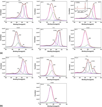
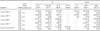
Figure 1(a) exhibited the XPS spectra (C1s and Sn3d5 scan) of the SnO x –Sn/graphene sensors fabricated at various temperatures of 150, 300, and 400 °C while the introduced O2 flux was kept at 1 sccm. Obviously, the formation of the compound SnO x (including SnO2 and SnO)–Sn films was demonstrated, which clearly indicated the existing components of the SnO2 (487.10 eV), SnO (486.13 eV), and Sn (484.70 eV) deconvoluted from the Sn3d5 scan spectra. The detailed analysis is listed in Table I, in which all the existing bonding states together with their binding energy and percentage content were presented. It was noteworthy that the content of the certain bonding state was usually represented by its peak area in the XPS spectra, which led to its normalized percentage content obtained by the calculation of its area percentage. The most interesting phenomena observed from Fig. 1(a) was that the content of the C–O–Sn bonding (285.73 eV) shown in the C1s scan spectra was monotonically reduced with the temperature increasing from 150 to 400 °C. The existence of the C–O–Sn bonding represented the chemisorptions of Sn, which involved the electron exchanging generated by the reaction between thermally evaporated Sn molecules and oxygen functional groups on the graphene surface. The monotonically decreasing C–O–Sn bonding content clearly indicated that the chemisorptions of Sn were suppressed with increasing fabrication temperature. Normally, with the increasing temperature, graphene functionalization would be greatly enhanced because more C–C/C=C bonds would be broken up and oxidized, and the main peaks centered at the binding energy about 284.80 eV were characteristics of graphitic carbon, representing the elemental sp2 and sp3 carbon atoms. However, in our case, the content of the C–C bonding (284.75 eV) was apparently raised with the fabrication temperature increased from 150 to 300 °C, which coincided well with the simultaneous decreasing of C–O–Sn bonding content. Meanwhile, the content of the ethers (C–O bonding) was almost unchanged. Such behavior of C–O–Sn, C–C and ethers demonstrated that the desorption of the oxygen functional groups on the graphene was dominant while the fabrication temperature increased from 150 to 300 °C, which resulted in the opposite variation of the content of the C–C bonding and C–O–Sn bonding as well as the stable ethers content. The enhancement of the oxygen functional groups desorption could be attributed to the vacuum annealing effect on the graphene substrate films in the thermal evaporation processing. It was reported that the vacuum annealing of graphene films would lead to the greatly straightened desorption of the oxygen species on the graphene surface. Reference Ni, Wang, Luo, Wang, Yu and Wu49–Reference Mulyana, Horita, Ishikawa, Uraoka and Koh52 The occurrence of such vacuum annealing effect could be demonstrated by the apparent blue shift of the 2D peak in the Raman spectra as shown in the inset of Fig. 1(a) (Sn3d5 scan at 300 °C), which indicated the obvious p-type doping of the graphene films after SnO x –Sn oxides deposition upon exposure to the air compared to the pristine graphene (p-graphene). Besides, no apparent densities of defects-relating D peak after Sn evaporation at 300 °C could be observed, indicating the perfect structure of the underneath graphene substrate films. In the thermal evaporation of Sn at a certain amount of O2 flux, the desorption of the oxygen functional groups together with the oxidation of the graphene and Sn should be both facilitated with the increasing fabrication temperature. However, at the lower temperature of 300 °C, desorption was dominant with the proof of the decreasing chemisorption of Sn (C–O–Sn bonding), increasing C–C bonding and almost stable ethers content. As the temperature further increased to 400 °C, the ethers content was dramatically raised while the C–C bonding and the chemisorptions of Sn (C–O–Sn bonding) were kept stable and dropping down, respectively. Therefore, the desorption of the oxygen functional groups and oxidation of the graphene both played critical roles at the higher temperature of 400 °C, resulting in the reduced chemisorptions of Sn (C–O–Sn bonding) and rising ethers as well as the almost unchanged C–C bonding content. Such assumption could also be supported by the variation of the SnO2 content observed from Sn3d5 scan spectra, which showed the opposite trend to that of Sn chemisorption (C–O–Sn bonding) and increased monotonically with fabrication temperature. Apparently, the chemisorptions of Sn on the graphene surface would hamper the formation of SnO2 because of the obstruction of the sufficient Sn oxidation. Meanwhile, considering the SnO and Sn content decreased monotonically with increasing temperature (the Sn content even reached null at 400 °C), there was no doubt that the Sn oxidation was facilitated with increasing temperature.
(a) XPS spectra (C1s and Sn3d5) of the SnO x –Sn/graphene sensors fabricated at various temperatures of 150, 300, and 400 °C with the O2 flux of 1 sccm; (inset in C1s at 300 °C: Raman spectra of pristine graphene (P-graphene) and SnO x –Sn/graphene sensor fabricated at 300 °C). (b) XPS spectra (C1s and Sn3d5) of the SnO x –Sn/graphene sensors fabricated at 300 °C with various O2 flux of 5 and 15 sccm.

Analysis of the XPS spectra of the SnO x –Sn films.

Figure 1(b) exhibited the XPS spectra of the SnO x –Sn/graphene sensors fabricated at 300 °C with various O2 flux of 5 and 15 sccm, which were compared with that of the 1 sccm O2 at 300 °C in Fig. 1(a). Apparently, the oxidation of the graphene films was greatly enhanced with increasing O2 flux from 1 to 15 sccm with the proof of the remarkable decreasing content of C–C bonding as shown in C1s scan spectra in Figs. 1(a) and 1(b) and Table I. The enhancement of the oxidation of graphene could also be demonstrated by the rising content of ethers with increasing O2 flux and the appearance of the C=O bonding (288.06 eV) in the case of the 15 sccm O2 flux. Such enhanced oxidation of the graphene imposed tremendous effect on the chemisorptions of Sn and the formation of SnO x . As shown in the C1s spectra and Table I, the content of the Sn chemisorptions (C–O–Sn bonding) increased initially with increasing O2 flux to 5sccm, and dropped down with the further increasing O2 flux to 15 sccm. Such behavior could be attributed to the inconsistency of the amount of the evaporated Sn and introduced O2 molecules during the thermal evaporation processing. In our case, the constant Sn evaporation rate would set up the maximum amount of Sn molecules possibly available in the chemisorptions with oxygen functional groups on the graphene. With the initial increasing O2 flux to 5 sccm, there was enough evaporated Sn molecules available for the Sn chemisorptions which led to the obvious increasing of the C–O–Sn bonding content. However, the thermal evaporation of Sn could not catch up the pace of the formation of oxygen functional groups on the graphene with the further increasing O2 flux to 15 sccm, which caused dramatical dropping of the Sn chemisorptions (C–O–Sn bonding) content. Such assumption could also be supported by the apparent increasing content of the ethers and the appearance of the C=O bonding resulted from the more serious oxidation of the graphene at 15 sccm O2 flux. It was noteworthy that the SnO2 content also exhibited the opposite variation trend to that of the C–O–Sn bonding content just like the case of increasing fabrication temperature previously discussed, which further proved that the chemisorptions of Sn would obstruct the formation of SnO2 due to the insufficient Sn oxidation caused, which led to the increasing content of SnO. Meanwhile, the Sn content dramatically reduced and no any Sn observed for the 5 and 15 sccm O2, which could be explained by the great facilitation of the Sn oxidization (formation of SnO and SnO2) with increasing O2 flux.
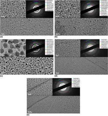
Figure 2 showed the TEM images of the SnO x –Sn/graphene sensors fabricated at various temperatures and O2 flux. Apparently, remarkable influence of the fabrication temperature on the SnO x –Sn film morphology could be observed. The SnO x –Sn films at a relatively low temperature of 150 °C exhibited densely packed, evenly distributed, fine nanoparticles with the average size around 10 nm, and most of the nanoparticles were isolated with the clear and separate boundaries [see Fig. 2(a)]. The domain boundaries from the underneath graphene was also clearly observed. With the fabrication temperature increasing to 300 °C, the coalescence and combination of the neighboring SnO x –Sn nanoparticles occurred, as shown in Fig. 2(b), and the average size of the SnO x –Sn nanoparticles was apparently enlarged, reaching about 20 nm. Such phenomenon could be ascribed to the routine “island growth” mode at early stage of the thermally evaporated films. Besides, the nanoparticles were not evenly distributed like in the case of 150 °C. Voids with the size about 10 nm were generated among the nanoparticles due to the combination of the neighboring nanoparticles and enhanced desorption of the oxygen functional groups at high temperature. Furthermore, the constant amount of evaporated Sn molecules reaching the graphene surface in the thermal evaporation processing made it impossible to catch up the growth of the SnO x –Sn nanoparticles and filled in the voids generated in films. Such assumption could also be used to explain the more striking variation of the SnO x –Sn film morphology at the fabrication temperature of 400 °C as shown in Fig. 2(c). SnO x –Sn nanoparticles with the uneven size (ranging from 10 to 50 nm) were sparsely distributed on the graphene surface and large voids (>50 nm) could be observed among the nanoparticles. As we previously assumed, in our thermal evaporation of Sn processing at a certain amount of O2 flux, the desorption of the oxygen functional groups as well as the oxidation of the graphene and Sn both imposed major effects on the SnO x –Sn film formation. Apparently, the desorption of the oxygen functional groups on the graphene together with the oxidation of Sn would be favorable for the growth of the SnO x –Sn nanoparticles and facilitate the formation of large grain-sized and discontinuous films. Meanwhile, such porous film morphology would be further promoted by the unvaried amount of Sn molecules available for the SnO x –Sn films at rising fabrication temperature, which resulted from the constant thermal evaporation rate applied. The morphology transformation from the densely packed, small grain-sized and compact SnO x –Sn films to sparsely distributed, large grain-sized and discontinuous ones proved that the above assumption was reasonable.
TEM images of the thermally evaporated SnO x –Sn films onto the graphene substrate films at various temperatures and O2 flux; (a) 150 °C, (b) 300 °C, (c) 400 °C with the O2 flux of 1 sccm; O2 flux of (d) 5 sccm, (e) 15 sccm at the temperature of 300 °C (inset: magnified images and SAD patterns).

The O2 flux during the thermal evaporation processing also demonstrated tremendous influence on the SnO x –Sn film morphology. More densely packed and smaller-sized SnO x –Sn nanoparticles could be observed with the O2 flux increased to 5 sccm compared to that of 1 sccm at the same fabrication temperature of 300 °C, as shown in Fig. 2(d). Such characteristics could be attributed to the enhanced chemisorptions of Sn and oxidation of graphene, which led to the formation of more C–O–Sn and ethers, as previously discussed and shown in the XPS results [see Figs. 1(a) and 1(b) and Table I]. Such strengthened Sn chemisorptions and graphene oxidation hampered SnO x nanoparticles further growth, which caused the formation of more densely packed and reduced-sized nanoparticles. It was noteworthy that the images with high magnification [see the inset in Fig. 2(d)] still exhibited the isolated SnO x –Sn nanoparticles with well-defined boundaries and gaps among them although the density of the nanoparticles on the graphene was greatly increased together with much reduced nanoparticles size. Such unique structure would impose tremendous influence on the SnO x –Sn/graphene hybrid sensor NO2 sensitivity. With the further increase of the O2 incorporation to 15 sccm, more vigorous variation of the SnO x –Sn film morphology could be observed as shown in Fig. 2(e). Very fine nanoparticles with ill-defined sizes were uniformly and densely distributed on the graphene surface. The nanoparticles were too small to be clearly distinguished from each other and no separate nanoparticles with well-defined boundaries could be found even in the high magnification image [see inset in Fig. 2(e)]. Apparently, the SnO x –Sn nanoparticles growth was remarkably restricted under high O2 pressure even at the high fabrication temperature of 300 °C, which could also be attributed to the increasing oxygen functional groups on the graphene surface due to the great enhancement of the graphene oxidation [see Figs. 1(a) and 1(b) and Table I]. Apparently, the influence of the oxygen functional groups was so overwhelming that the SnO x –Sn nanoparticles had no any chance to grow to noticeable size, which agreed well with the XPS results previously presented.
Selective area diffraction (SAD) patterns of the SnO x –Sn films thermally evaporated at various temperatures and O2 flux was used to characterize the film structure, as shown in the insets of the Fig. 2. The rings marked with color arcs were indexed to tetragonal rutile SnO2 and SnO planes while the red arrows represented the {100} and/or {110} type reflections of graphene. The formation of SnO x –Sn compound at the temperature of 150 °C with the 1 sccm O2 flux could be demonstrated by the SAD pattern in Fig. 2(a), in which the diffraction rings from the SnO (101), SnO2 (204), (134) and (312) as well as the Sn (220) could be observed. Such SAD pattern coincided very well with the corresponding XPS results previously presented. With the further increasing temperature to 300 °C, SAD pattern exhibited apparent variation as shown in Fig. 2(b). The broad blurry ring for SnO (101) at the temperature of 150 °C transformed to sharp and bright one, and the sharp ring for SnO2 (204) changed to elongated dots, both of which were typical evidences to indicate that the high fabrication temperature would promote the crystallization of the SnO x –Sn films. Such improved crystallization at high temperature could be further supported by the SAD pattern of the SnO x –Sn films at 400 °C [see the insets in Fig. 2(c)], as evidenced by the sharp and bright diffraction rings of various SnO and SnO2 planes as well as the total disappearance of the diffraction of Sn, which also agreed well with the previous XPS results. The formation of the enhanced polycrystalline SnO x –Sn films could be ascribed to the increasing mobile energy of vapor molecules on the graphene substrate surface supplied by substrate temperature. At low temperature, the mobility of the adsorbed species on the graphene substrates was relatively low, thus preventing those species from migrating to more energetic sites where nucleation could occur. With the increasing fabrication temperature, the adsorbed species would acquire enough energy for migrating and crystallization, and finally form large grain-sized SnO x nanoparticles on the graphene surface [see Fig. 2(c)].
On the contrary, the increasing O2 flux at the fixed temperature of 300 °C would obstruct the polycrystallization of the SnO x –Sn films due to the formation of the tiny-sized and compact nanoparticles as shown in the corresponding TEM images. Such deterioration of the crystallization could be supported by the typical broad and fuzzy diffraction rings like SnO (101) and SnO2 (204) as shown in the insets in Figs. 2(d) and 2(e). The reduction of the crystallinity with the introduction of oxygen was also observed in other metal oxides, which could be attributed to the segregation of oxygen in the grain boundaries and decreasing of the grain boundaries mobility. Reference Al-Kuhaili53,Reference Adamik, Barna, Tomov and Biro54 Meanwhile, the total oxidation of Sn was also demonstrated by the vanishing of the Sn diffraction rings, consistent with the corresponding XPS results. It was also noteworthy that the SAD patterns were much simplified with the increasing O2 flux. Apparently, the improved orientation of the crystalline SnO x –Sn films was achieved with the increasing O2 flux due to the obstruction of the nanoparticles growth at high O2 pressure. The suppressed growth prevented the disorientation inevitably occurred in the growth processing, just like what happened at high temperature of 400 °C.
B. NO2 sensitivity of the SnO x –Sn/graphene hybrid sensors
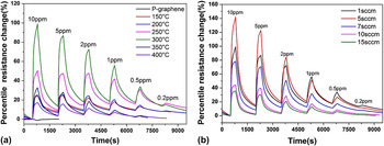
The sensitivity dependence on the fabrication temperature was shown in Fig. 3(a) and Table II. It could be found that the NO2 sensitivity of the SnO x –Sn/graphene hybrid sensors was improved dramatically compared to that of the pristine graphene (P-graphene) and the apparent p-type (P-graphene) to n-type (SnO x –Sn/graphene) response transformation occurred. Besides, the hybrid sensor NO2 sensitivity enhanced with increasing temperature up to 300 °C and then deteriorated with further increasing temperature to 400 °C, which made the 300 °C be the optimal temperature. In our hybrid sensors, the SnO x acted as reaction centers for the target NO2 gas while the substrate graphene films were applied as conductive networks for carriers transporting. SnO2 as widely recognized n-type metal oxide gas sensors demonstrated superior response to both reducing and oxidizing gases Reference Yamazoe, Sakai and Shimanoe30 and NO2 was a typical oxidizing gas. The interaction between the oxygen adsorbates on the SnO2 surface and NO2 molecule would lead to the electron transferring from SnO2 to NO2 and cause the increasing SnO2 film resistance. A higher sensitivity resulted from more NO2 molecules adsorption and more electrons transferring. However, for the traditional bulk-sized SnO2 materials, normally higher working temperature over 200 °C was needed for superior gas performance because their relatively low conductivity at room temperature resulted from the semiconductor nature and higher temperature required for the generation of oxygen adsorbates on the SnO2 surface. Reference Yamazoe, Sakai and Shimanoe30,Reference Barsan and Weimar55 In our case, the application of high conductive graphene films as carriers transporting network greatly facilitated the transducer function. Besides, it was reported that the oxygen adsorbates were also possibly generated at room temperature. Reference Yamazoe, Sakai and Shimanoe30 Therefore, the unique structure of SnO x –Sn/graphene made the detection of NO2 at room temperature possible. It was also widely considered that the gas sensing performance of the metal oxides had strong dependence on their composition and morphology. Reference Yamazoe, Sakai and Shimanoe30,Reference Deng, Tjoa, Fan, Tan, Sayle and Olivo56–Reference Srivastava, Jain, Singh, Singh, Vijayan and Dilawar58 In our case, the desorption of the oxygen functional groups on the graphene surface together with the oxidation of Sn and graphene were both enhanced with increasing fabrication temperature and resulted in the variation of film morphology and composition. Since the SnO x content increased monotonically with temperature, which was inconsistent with the temperature dependence of the NO2 sensitivity, the effect of SnO x –Sn film composition on their sensitivity was quite limited. On the other hand, as shown in Fig. 2, striking influence of the fabrication temperature on the morphology could be observed which varied from densely packed, small-sized, and compact films to the sparsely distributed, enlarged-sized and discontinuous films with increasing temperature. Hence, the morphology of the SnO x –Sn films had to impose the vital influence on the hybrid sensor sensitivity. It was well known that the metal oxides with small grain size and porous structure demonstrated superior gas sensing performance compared to those with large grain-sized and compact structure. Reference Yamazoe, Sakai and Shimanoe30,Reference Zhang and Liu59,Reference Zhao, Choi, Kim and Hong60 Such influence could be explained by the specific surface area of the metal oxides and the penetrating depth of the target gas inside the metal oxides, both of which would be greatly enhanced for small grain-sized and porous structure, and resulted in more serious reactions between oxygen adsorbates and target gas on the metal oxide surface. In our case, the SnO x –Sn films at 300 °C obtained the optimized SnO x –Sn nanoparticle size as well as the porous enough structure for the NO2 penetrating. Such optimal structure maintained enough specific surface areas on the SnO x –Sn nanoparticles as active sites for the reaction between oxygen adsorbates and NO2 as well as porous enough structure for the easy penetrating of the NO2. On the contrary, for the hybrid sensors fabricated at 150 °C, the compact SnO x –Sn films obstructed the NO2 penetrating although the nanoparticles size was small. Meanwhile, the sparsely distributed and large grain-sized nanoparticles at high fabrication temperature of 400 °C could not provide large enough specific surface areas on the SnO x –Sn nanoparticles as reaction centers in spite of the easiness of the NO2 to reach the SnO x –Sn nanoparticles due to the abundance of the large voids inside the SnO x –Sn films.
The sensitivity of the SnO x –Sn/graphene hybrid sensors fabricated at various temperatures and O2 flux upon the exposure to various concentration of NO2; (a) temperature ranging from 150 to 400 °C with the O2 flux of 1 sccm; (b) O2 flux ranging from 1 to 15 sccm at the temperature of 300 °C.

Sensitivity performance of the SnO x –Sn/graphene hybrid sensors.

In addition, the improvement of the sensing performance of the SnO x –Sn/graphene hybrid sensors might be attributed to the contribution of the heterojunction formed at the interface between SnO x and graphene. It was reported that upon the exposure to air, the first depletion layer was formed by the oxygen adsorbates (O2−) at the surface of the SnO x nanoparticles, while the second one was caused by the SnO x –graphene heterojunction. Reference Tang, Lee, Xu, Liu, Chen, He, Cao, Yuan, Song, Chen, Luo, Cheng, Zhang, Bello and Lee61,Reference Zhang, Feng, Fei, Liu and Zhang62 The reactions between the NO2 and oxygen adsorbates on the surface of the SnO x nanoparticles not only modified the first depletion layer but also altered the second one at the SnO x -graphene interface, which led to the effective electronic interaction between SnO x and graphene, and therefore facilitated NO2 detection. Since such performance heavily depended on the adsorption, desorption, and surface reactions at the SnO x and graphene surface, the surface accessibility of the SnO x –Sn/graphene hybrid sensors was crucial for their sensitivity. Therefore, the morphology of the SnO x –Sn films was critical for the hybrid sensor sensitivity, as previously discussed, and the deposition of SnO x –Sn nanoparticles onto the graphene surface generated more active sites for the adsorption of NO2 molecules and led to superior sensitivity.
The sensitivity dependence on the O2 flux was shown in Fig. 3(b) and Table II. The NO2 sensitivity of the SnO x –Sn/graphene hybrid sensors was promoted with increasing O2 flux to 5 sccm and then dropped down with further increasing to 15 sccm, which made the 5 sccm be the optimal O2 flux for NO2 sensitivity. As we previously presented, the O2 flux during the thermal evaporation processing also imposed tremendous influence on the SnO x –Sn film morphology as well as their composition and structures. More densely packed and smaller-sized SnO x –Sn nanoparticles could be observed with the O2 flux increased to 5 sccm compared to that of 1 sccm at the same fabrication temperature of 300 °C, as shown in Fig. 2(d). However, the SnO x –Sn nanoparticles were still isolated with well-defined boundaries and gaps among them. Such characteristic structure guaranteed the simultaneous possession of the abundant SnO x –Sn reaction centers and easy access for the target NO2 gas diffusing inside the SnO x –Sn films due to the coexistence of large specific surface area and penetrating depth, which achieved the optimal sensitivity performance of 140% response upon the exposure to 10 parts per million (ppm) NO2 as well as the low detection limit of 200 parts per billion (ppb) at room temperature. With the further increasing of the O2 flux to 15 sccm, much more vigorous variation of the SnO x –Sn film morphology could be observed as shown in Fig. 2(e). Very fine nanoparticles with ill-defined sizes were uniformly and densely distributed on the graphene surface. Such extremely densely packed and fine nanoparticles films would greatly hamper the NO2 penetrating inside films, which caused the apparent deterioration of the gas sensitivity.
The response time of the hybrid SnO x –Sn/graphene sensors increased with fabrication temperature to 300 °C, and dropped down with further temperature increasing to 400 °C as indicated in Table II. Since the response time in our case was defined as time needed for the resistance change from 10% to 90% of the maximum, and the response at 300 °C (99.1%) was much larger compared to those of at 150 (24.8%) and 400 °C (17.3%), a little longer response time corresponding to much high performance could be resulted from the longer time needed to reach the sensitivity saturation due to the more reactions between the SnO x –Sn nanoparticles and NO2 involved. Similar trend was also discovered for the performance of the recovery. The recovery of 86.4% in 20 min was obtained for the hybrid sensors fabricated at 300 °C without any heating required, which could be ascribed to the almost defect-free structure of the SnO x –Sn/graphene films as demonstrated by the Raman spectra in Fig. 1(a) as well as the porous structure for the good gas permeability.
The influence of the O2 flux on the response time and recovery was also exhibited in Table II. The response time decreased with increasing O2 flux to 7 sccm and showed little difference beyond that. Considering the relatively comparable response of the hybrid sensor fabricated at 1 sccm (99.1%) and 5 sccm O2 (142.1%), a little improvement of the response time of the one at 5 sccm O2 (147 s compared to 168 s) probably resulted from the large specific surface area of its fine nanoparticles, which facilitated the reactions between the oxygen adsorbates and NO2 on the SnO x surface. Meanwhile, more densely packed and finer nanoparticles would be generated with further increasing O2 flux, which not only deteriorated the response due to the obstruction of the NO2 penetrating inside the SnO x –Sn films but also minimized the influence of the morphology on the response time because of the limited NO2 penetration. Hence, almost unvaried response time was observed. Besides, the recovery close to 90% at room temperature without heating also demonstrated the superior structure of the hybrid SnO x –Sn/graphene sensors.
There were other reports regarding the graphene-based hybrid NO2 gas sensors, such as RGO conjugated Cu2O nanowires, Reference Deng, Tjoa, Fan, Tan, Sayle and Olivo56 indium (In)-doped SnO2 nanoparticle-graphene nanohybrids Reference Cui, Wen, Mattson, Mao, Chang and Weinert57 and graphene–WO3 composites. Reference Srivastava, Jain, Singh, Singh, Vijayan and Dilawar58 Our SnO x –Sn/graphene hybrid sensors exhibited better sensitivity and faster response compared to those of the RGO–Cu2O nanowires at the room temperature while the In-doped SnO2–graphene demonstrated better sensitivity but much more inferior response time and recovery. The graphene–WO3 composites exhibited comparable and faster response but at the optimal high temperature of 250 °C, which would complicate the sensor designation and cause inconvenience in sensor application. Hence, our SnO x –Sn/graphene hybrid sensors proved superior comprehensive performance in NO2 detection compared to those similar hybrid graphene-based sensors.
IV. CONCLUSIONS
The SnO x –Sn/graphene hybrid NO2 gas sensors were fabricated by thermal evaporation and the effect of fabrication temperature and O2 flux on their properties and NO2 sensitivity was investigated. The compound SnO x –Sn films consisting of SnO2, SnO, and Sn on the graphene substrate films demonstrated strong composition, morphology, and structure dependence on the fabrication temperature and O2 flux, which resulted from the synergic effect of the desorption of the oxygen functional groups and the oxidation of the graphene and thermally evaporated Sn. The improved sensitivity of the SnO x –Sn/graphene sensors could be ascribed to their hybrid structure, in which SnO x –Sn and graphene acted as high sensitivity reaction centers and effective carriers transporting networks, respectively. The morphology of the SnO x –Sn films would impose vital influence on the hybrid sensor NO2 sensitivity, and the optimized structure obtained at 300 °C and 5 sccm O2 flux possessed enough specific surface areas on the SnO x –Sn nanoparticles as reaction centers as well as porous enough structure in the SnO x –Sn films for the good permeability of NO2. We expect that this hybrid structure will provide a practical option for the future preparation of high performance graphene-based NO2 gas sensors.