I. INTRODUCTION
Miniaturizing and high-density packaging of microelectronic devices are responsible for making electromigration (EM)Reference Chen, Tong and Tu1,Reference Chen and Liang2 and thermomigration (TM)Reference Chen, Tong and Tu1,Reference Zhang Jin-Song, Yong-Guo and Yuan3,Reference Ouyang and Jhu4 two of the most persistent reliability issues in interconnections. TM usually occurs with EM when a sufficient thermal gradient is created, caused by the inhomogeneous distribution of Joule heating.Reference Chen, Tong and Tu1,Reference Gu, Yung, Chan and Yang5–Reference Gu and Chan7 In a real solder joint, the nonuniform Joule heating mainly stems from the geometrical configurations and the chip side produces much more heat than the substrate side.Reference Chen and Chen8 As a result, a thermal gradient can be formed across the solder joint, resulting to TM. A nonuniform Joule heating can also be formed in a heterogeneous microstructure, due to the resistivity divergence of the different phases involved.Reference Guo, Xu, Sun, Xia, Lei, Shi and Li9 The critical thermal gradient value, that is sufficient to trigger TM, is generally considered to be the 1000 °C/cm,Reference Chen, Tong and Tu1 although some previous studies have reported that a value of ∼400 °C/cm could also result to TM.Reference Chen, Chen and Tu10 Various studies suggest that the thermal gradient may be the only necessary condition for the formation of TM. Also, the ambient temperature factor contributes positively to the formation of TM, because the diffusion process is a temperature-dependent process. However, this statement has not been experimentally demonstrated yet.
Various studies have previously addressed the issues related to the EM and TM in solder joints.Reference Zhang Jin-Song, Yong-Guo and Yuan3–Reference Chen and Chen8,Reference Chen, Chen and Tu10–Reference Hsu and Ouyang18 Most of them were focused on conventional SnPb solder joints,Reference Chen, Tong and Tu1,Reference Huang, Gusak, Tu and Lai17 or Sn-based solder joints.Reference Wei, Du, Jia and Qi12,Reference Ouyang and Kao14–Reference Lin, Tsao, Liang and Chen16 Huang et al.Reference Huang, Gusak, Tu and Lai17 discovered that in a composite SnPb solder joint, where Sn97Pb was observed in the warmer side of the joint and eutectic Sn63Pb on the colder, Pb had migrated to the colder side and Sn to the warmer. For Sn-based solder joints, the major migration chemical constituents that were induced by TM were believed to be Cu or Ni, based on the Cu–Sn or Ni–Sn system. Wei et al.Reference Wei, Du, Jia and Qi12 reported that TM had caused interfacial accumulation of intermetallic compounds (IMCs) to the colder side of the solder joint and disintegration at the warmer. This comes to an agreement with Qu et al.,Reference Qu, Zhao, Ma, Zhao and Huang13 where he observed the same phenomenon between the liquid–solid state of Cu/Sn/Cu solder joints. Unusual Ni3Sn4 interfacial growth at the colder side was reported by Ouyang et al.Reference Ouyang, Jhu and Chang15 However, the formation of TM of Ni–Sn IMCs demands a higher thermal gradient than that of the Cu–Sn IMCs.Reference Hsu and Ouyang18 In addition, the TM of Cu or Ni was significantly affected by the anisotropic behavior of Sn.Reference Hsu and Ouyang18 The c-axis of Sn grains, which is parallel to the direction of the thermal gradient, would cause the maximum TM diffusion of Cu or Ni. Furthermore, the TM in Sn58Bi solder joints has also been reported in the literature,Reference Gu, Yung and Chan6,Reference Gu and Chan7 where Bi-atoms tend to migrate towards the colder side.
Although the kinetics of the faster migration elements (Pb, Bi, Cu, and Ni) in solder joints is well described and explained, the TM of Sn atoms is seldom observed directly. Ouyang et al.Reference Ouyang and Kao14 was the first to observe the presence of Sn atoms to the warmer side of the solder joint in a Sn3Ag0.5Cu alloy by making indentation diffusion markers. The direct evidence for this observation is still missing. Two major reasons are responsible for the difficulty to examine the Sn fluctuation in solder joints. First, the use of phase contrast of migrated Sn phases and Sn matrix in Sn-based solder joints are the same and it is difficult to distinguish them. Secondly, if the electron flow is parallel to the direction of thermal gradient, then the TM may assist or interact with the EM. Therefore, distinguishing between the contribution of TM and EM is considered as a great challenge, mainly because of their overlapping effects.
To provide a solution to this issue, the present study is focused on designing a linear symmetry in the solder joint structure, which could orient the direction of the thermal gradient perpendicular to the electron flow. The thermal gradient could be observed when coupled with the infrared imaging technique. Different ambient temperatures were considered during the experimental procedure. In addition, since Joule heating is sensitive to microstructural changes, this study attempted to establish the relationship between the temperature distribution and microstructural evolution. In this way, some of the microstructural characteristics in solder joints, such as void formations, could be revealed by the temperature distribution. The results will be beneficial to better understanding the behavior of TM and EM and the fundamental principles that govern them.
II. EXPERIMENTAL PROCEDURE
A. Materials
In the present study, two types of samples were used. The schematics of type A and type B samples are presented in Figs. 1(a) and 1(b), respectively. Both of them were manufactured by a linear Cu/Sn58Bi/Cu solder joint, using two copper plated heat sinks at the end of the substrate. The configuration of the linear solder joint was right-angled, isosceles triangular prism, as shown in Fig. 1(a). The hypotenuse of the triangular cross-section was 447 μm wide, the length of the solder joint was 500 μm long and the resultant cross-section area of the solder joint was 5 × 10⁻⁴ cm2. When applying an electric current of 5 A on the sample, the calculated current density could reach up to 104 A/cm2 on the solder joint. Both, type A and type B samples had the same solder joint dimensions, but different heat sink values. The area of heat sink in type B was 5 times larger than in type A. Both type A and type B samples were mounted in epoxy resin, according to standard specimen preparation procedures that will allow subsequent sample testing and characterization. Further details of sample preparation procedure can be found in a previous study.Reference Zhang, Xu, Wang, Guo, Lee and Subramanian19
Configurations and FEM simulations of type A and type B samples: (a and b) schematics of solder joints and (c and d) temperature distribution.

B. Experimental setup and characterization
The different heat sinks of the plates of type A and type B samples will assist on recognizing the effect of the magnitude of Joule heating on TM, since the sample with the larger heat sink facilitates heat sinking and reduces the magnitude of Joule heating which is accumulated on the solder joint. The finite element analysis (FEM) results of the temperature distribution in type A and type B samples is presented in Figs. 1(c) and 1(d), respectively. The module used in FEM was the Thermal-Electric, ANSYS 15.0. The ambient temperature and applied electric current were 20 °C and 5 A, respectively. Thermal conductivity of Sn58Bi, copper, and epoxy used in FEM were 30, 401, and 1.5 W/m oC, respectively. The convection coefficient of thermal conductivity of materials used in FEM was 2 W/m2 °C. FEM results indicated that the maximum temperature in Type A sample was 3.5 °C higher than that of type B sample.
Three testing groups were designed for this experiment. In the first group, type A samples were used at a current density of 104 A/cm2 and at room temperature. In the other two groups, different types of sample were used at a current density of 104 A/cm2 and at a temperature of 50 °C. The experimental design was such that the effects of both temperature and magnitude of Joule heating on TM could be related. Both the microstructural evolution and the temperature distribution of solder joints were examined after each going through a period of testing. Scanning electron microscopy (SEM) was used for the microstructural evolution, while the temperature distribution was measured by thermal infrared microscopy (IR), at a temperature resolution of 0.1 °C and a spatial resolution of 2 μm. IR examined for all samples were operated at 20 °C.
III. RESULTS
A. Microstructure and temperature distribution at room temperature
Figure 2 shows the microstructural evolution and temperature distribution of a type A sample, with a current density of 104 A/cm2, at room temperature. In Fig. 2(a), the microstructural characteristics of the as-reflowed solder joint can be defined as fine and uniform. The corresponding IR image presents a symmetrical distribution of the temperature, as shown in Fig. 2(b). Across the vertical direction, a higher temperature is observed close to both edges. Along the horizontal direction (parallel to the electron flow), the temperature of the two interfaces is much lower. In Fig. 2(c), cracks initiation was formed on the surface of the solder joint, after suffering the current stress for 10 d. These cracks can also be observed in the corresponding IR image. As indicated in Fig. 2(d), higher temperatures were observed around the cracks, because the crack caused current concentration. As the time was increased to 25 d, the cracks propagated further, as shown in Fig. 2(e). A much higher intensity of current concentration resulted in an increase of the temperature adjacent to the crack [see Fig. 2(f)]. Besides, the temperature distribution increasingly transited from a contour line pattern to a mixture pattern, as seen in Figs. 2(b), 2(d) and 2(f).
Microstructural evolution and temperature distribution of a type A sample at room temperature: (a and b) as-reflowed; (c and d) 10 d; (e and f) 25 d.
B. Microstructure and temperature distribution at 50 °C
Figure 3 shows SEM and IR images of a type A sample that was exposed to a current density of 104 A/cm2, at 50 °C. Similarly to Figs. 2(a) and 2(b), the microstructure and temperature distribution of Figs. 3(a) and 3(b) was uniform and symmetrical in the as-reflowed specimens. After 42 h, the surface morphology changed significantly, as shown in Fig. 3(c). A crack formed in the center of the solder joint, while a few clusters of Sn-rich phases were observed across both edges of the vertical direction. Additionally, the solder joint significantly overflowed at both interfaces. This phenomenon indicates that the solder joints had already been re-melted locally. IR images further support this theory. As shown in Fig. 3(d), the temperature at the crack location exceeded the melting point of the Sn58Bi solder joint. As time was further increased, no obvious changes were observed in the surface morphology, but the temperature continued rising, which can be attributed to the Joule heating accumulation.
Microstructural evolution and temperature distribution of a type A sample at 50 °C: (a and b) as-reflowed; (c and d) 42 h; (e and f) 45 h.
The microstructural evolution and temperature distribution of a type B sample is presented in Fig. 4. When compared to Fig. 3, the type B sample of Fig. 4 demonstrated similar results to the type A sample. However, the average size of the clusters of the Sn-rich phase across the edges of the vertical direction was smaller and the temperature increased, as Joule heating was lower in the type B sample. Also, although no failure was detected in the center of the SEM image of Figs. 4(c) and (e), the corresponding IR images of Figs. 4(d) and (f) show a region with an unusual temperature increase in the center area of the sample. It is suggested that void formation took place in the center of the sample, resulting into current concentration.
Microstructural evolution and temperature distribution of a type B sample at 50 °C: (a and b) as-reflowed; (c and d) 42 h; (e and f) 45 h.
IV. DISCUSSION
The IR images of the as-reflowed samples in Figs. 2–4 present symmetrical patterns of temperature distribution, which were attributed to the heat sinking structures of the solder joints. Joule heating could dissipate along the horizontal direction through heat sinks at the end of copper substrates. However, Joule heating was difficult to dissipate across the vertical direction because of the poor conductivity of the adjacent epoxy. Consequently, a special pattern of thermal gradient was established on the solder joint. The vertical direction was only influenced by the thermal gradient that was extended from the center to the edges, while the horizontal direction was more complexly affected. Apart from the thermal gradient from both the interfaces to the center of the sample, the solder joint also suffered the electron wind force from the cathode to anode. Obviously, this pattern of thermal gradient assisted on analyzing the TM across the vertical direction and the coupling effect of both TM and EM, along the horizontal direction. Although temperature distribution varied with time, the as-reflowed temperature distribution was critical to analyze the subsequent microstructure change because it provided initial drive force for TM. Therefore, the following discussing mainly focus on the temperature distribution at the as-reflowed state.
A. Relationship between microstructure characteristics and temperature distribution
Since the evolution of the microstructure evolved with the ongoing EM and TM, the corresponding IR images demonstrated a sensitive response to the changing of the microstructural characteristics. The crack initiation and propagation in Figs. 2(c) and (e), Figs. 3(c) and (e) and the void formation in Fig. 4 were well depicted by the IR images, due to the current concentration effect. Moreover, phase coarsening and segregation were also observed due to the resistivity divergence. In Fig. 2, the fine, uniform microstructure was increasingly becoming coarser and segregated under room temperature conditions. The corresponding IR images were also changed from a symmetrical to a heterogenetic pattern. Especially in Fig. 2(f), the contoured thermal gradient that had initially appeared in Figs. 2(b) and 2(d) almost disappeared and was replaced with a mixed pattern. This can be attributed to the size of the Sn-rich and Bi-rich phases, which became coarser and the difference could be detected by IR. The results demonstrated that the microstructural characteristics could be well described by the pattern of the temperature distribution.
B. Effect of ambient temperature on TM
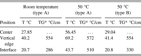
Across the vertical direction, the center of the sample was at a lower temperature and the edge as a higher, therefore a thermal gradient was formed with a direction from the edge to the center. As seen in Table I, the vertical thermal gradient at both room temperature and 50 °C of the type A samples had similar values, 554 and 572 °C/cm, respectively. However, this magnitude of thermal gradient was able to cause TM of Sn atoms at 50 °C, but not at room temperature. At 50 °C, as seen in Fig. 3(c), Sn atoms migrated from the center to the edge of the sample, forming the continuous Sn-rich phases at the edge and leaving voids at the center of the sample. At room temperature there was no migration of Sn atoms observed, although the high level of thermal gradient was maintained for 25 d. This implies that the thermal gradient was not the only factor that caused TM, but elevated temperature was also needed.
Average thermal gradient at the as-reflowed samples.
C. Effect of the magnitude of Joule heating on TM
Comparing the SEM images in Figs. 3 and 4, it is observed that the size of the clusters of the Sn-rich phases across the vertical edges, in the type B sample, was much smaller than in the type A, meaning that there were less Sn atoms migrated from the center to the edge of the sample. The reason for this was that the type B sample, which had the largest heat sink, assisted on dissipating Joule heating in the solder joints. Dissipation of Joule heating had a binary effect. On the one hand, the actual temperature on the solder joint was decreased. Comparing the IR images in Figs. 3 and 4, the temperature levels of the type B sample, at various phases, were all lower than those of the type A sample. On the other hand, Joule heating dissipation also reduced the thermal gradient, which means that the driving force of TM was lowered. As seen in Table I, the vertical thermal gradient of the type B sample was relatively lower than that of the type A sample, at 50 °C, namely 554 and 572 °C/cm, respectively. This indicates that TM is strongly dependent on the magnitude of Joule heating that is accumulated in the solder joint.
D. TM mechanism of the Sn atoms
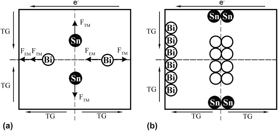
In Sn58Bi solder joints, Bi is usually the prior migration element, regardless the EM or TM conditions. It can be easy to observe that the Bi phases segregate at the anode during EM,Reference Guo, Xu, Sun, Xia, Lei, Shi and Li9 or at the region with the lower temperature during TM.Reference Gu, Yung and Chan6,Reference Gu and Chan7 In this study, unusual TM of Sn atoms across vertical edges was observed. The reason was attributed to the combined effect of the EM along the horizontal direction and the TM across the vertical direction. A schematic drawing of both EM and TM was introduced in Fig. 5 to clearly demonstrate this combined effect.
Schematic drawing of (a) EM and (b) TM in Sn58Bi solder joint.
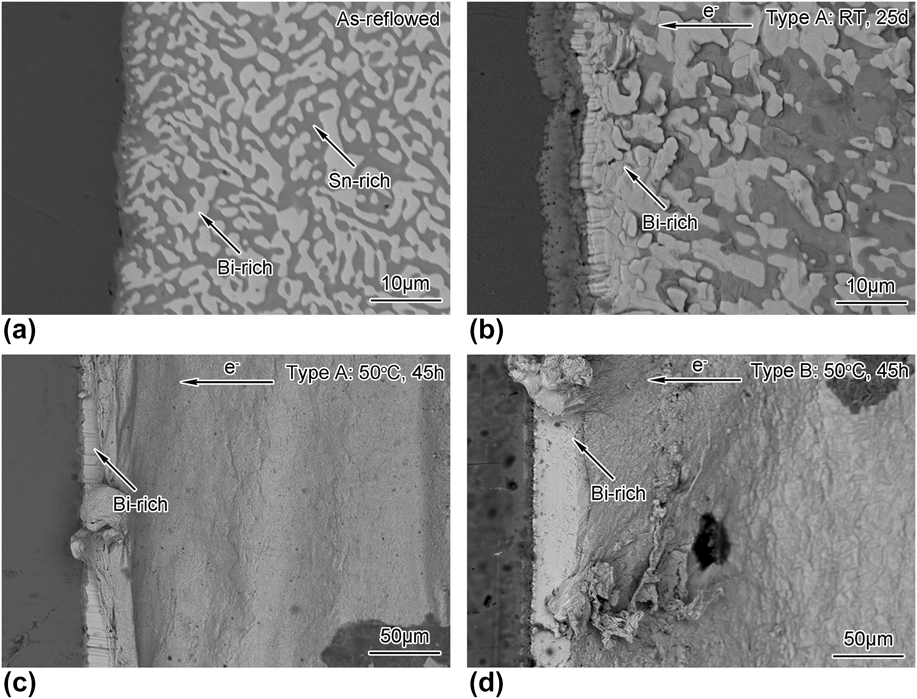
In the horizontal direction, metal atoms suffered electron wind force and thermal gradient simultaneously. Firstly, since the electrical current flowed from the right side to the left side, there was an EM flux formed across the solder joint with the driving of electron wind force. Secondly, the thermal gradient was established from the center to each side of interface due to the temperature at the center was higher than each side. As a result, Bi-atoms tended to move from the hot side to the cold side while Sn atoms moved in the opposite direction. It was observed that, only Bi was discussed in this direction because Bi was the main migration element. As seen on the left of Fig. 5(a), the thermal gradient and electron flow were of the same direction. It is believed that Bi-atoms were migrating towards the side with the lower temperature. Therefore, both EM and TM enhanced the Bi migration to the left-sided interface, forming a continuous Bi-rich layer. Figure 6 presents the results of segregation of the Bi-rich phase. At room temperature, Bi atoms were inclined to migrate towards the left-sided interface, where there were already some Bi-rich phases observed. At 50 °C, a Bi-rich layer could be clearly observed at the left side, which was both driven by EM and TM. At the right side, the direction of thermal gradient and electron flow were contradictory, where EM was partly overlapped by TM. As the net Bi flux was minimal, no obvious microstructural changes were observed at the right side.
Microstructures at anode side: (a) as-reflowed; (b) type A sample exposure to room temperature for 25 d; (c and d) type A and type B samples exposed to 50 °C for 45 h, respectively.
Across the vertical direction, there was only observed thermal gradient from the edge to the center, as shown in Fig. 5(a), while Sn atoms were believed to migrate towards the warmer side. Thus, Sn atoms were driven by the thermal gradient and segregated across the edges. It is clear that, if only the thermal gradient is exerted in a Sn58Bi solder joint, it should be the Bi-atoms that would migrate to the center (the side with the lower temperature), since this element is the fastest, as previously mentioned. However, only Sn-rich phases were observed in this case. This is attributed to the fact that Bi-atoms preferentially migrate towards the left interface and only Sn atoms were left at the center of the sample. Regarding the horizontal direction, both TM and EM were the driving forces of the Bi atoms towards the left-sided interface. Also, there was almost no migration of Bi-atoms from the right side, because of the overlapping between EM and TM. Therefore, there were no sufficient Bi-atoms to diffuse across the vertical direction. At this point, Sn flow became the main migration factor.
As Bi-atoms were migrating towards the left side and Sn atoms were diffusing to the vertical edge, vacancies consequently aggregated at the center, as shown in Fig. 5(b), and even better in Figs. 3 and 4. In Figs. 3(c) and 3(e), voids aggregated and eventually resulted into a crack. Similar phenomenon was observed in Figs. 4(d) and 4(f). Although voids could not be observed directly following SEM analysis [Figs. 4(c) and 4(e)], the unusual high temperature that appeared in the center of the sample proves that there were void formations in this area.
V. CONCLUSIONS
In this study, a linear symmetry solder joint structure, which could turn the direction of thermal gradient perpendicular to the electron flow, was used to examine the effect of TM and EM on Sn58Bi solder joints. The microstructural evolution and temperature distribution were analyzed and discussed comprehensively. The results indicated that, the microstructural characteristics could be well described by the pattern of temperature distribution. Elevated temperature and sufficient thermal gradient were two essential factors that caused TM, while a higher Joule heating facilitated TM process. Unusual TM of Sn atoms across vertical edges was attributed to the combined effect of EM along the horizontal direction and TM across the vertical direction.
ACKNOWLEDGMENTS
The authors would like to acknowledge the support of this work from National Natural Science Foundation of China (51301007) and Beijing Nova program (xx2016118).