Introduction
Since the Internet of Things (IOT) is widely paid attention by national governments, academia, and industry, the wireless communication based on ultra-wideband (UWB) technology can also be applied to implement the industrial IOT [Reference Wang, Mei and Wei1]. In this technology, UWB band-pass filters (BPFs) with good in-band performance, and high selectivity have become highly desired. Several methodologies have been proposed for the design of UWB BPFs in recent years.
A simple approach for a UWB BPF was proposed to create transmission zeros below 3.1 GHz and above 10.6 GHz [Reference Ishida, Araki and Other2]. However, this BPF has a large circuit size and a narrow bandwidth at the stop band because of the nature of band-pass behavior at twice the center frequency (2f 0). To overcome this limitation, the electromagnetic bandgap structure was used to suppress the harmonic response and extend the stopband in [Reference Garcia-Garcia, Bonache and Martin3]. Other techniques using cascaded low-pass (or band-pass) and high-pass (or band-stop) filters to improve upper stopband performance have been reported in [Reference Tang and Chen4, Reference Hsu, Hsu and Kuo5]. Although these UWB BPFs have a wide upper stopband and good selectivity, their insertion losses and overall size are inevitably increased. To reduce the circuit size, the hybrid microstrip/coplanar waveguide (CPW) structure has been adopted with a compact footprint in [Reference Abbosh, Bialkowski and Ibrahim6]; however, this type of BPF may suffer from a poor harmonic response and its upper stopband needs to be further improved. Another way to implement compact UWB BPFs is based on a multilayer low-temperature co-fired ceramic (LTCC) technology [Reference Almorqi, Shaman and Alamoudi7]. However, the fabrication of a multilayer circuit is much more complex than that of a single-layer circuit and therefore may not be convenient for system integration.
To design a small UWB BPF on a single layer with good out-of-band selectivity and harmonic rejection, the concept of a multiple-mode resonator (MMR) with a stepped-impedance configuration is utilized to construct a UWB BPF [Reference Zhu, Sheng and Menzel8]. Unlike traditional BPFs with parallel-coupled resonator, which use a single resonant mode, MMR-based BPFs are designed by allocating the first few resonant frequencies to the wide (desired) passband and setting the coupling peak of the quarter-wave parallel-coupled lines at the center frequency. These BPFs have many attractive features, such as a simple design, a compact size, a low loss, a flat group-delay in the UWB, and easy integration with other circuits/antennas. Therefore, the MMR technique is an important method for the design of UWB BPFs. In [Reference Xiong, Teng, He, Tam, Yu, Choi and Chen9–Reference Hao and Hong11], many MMR UWB BPFs with improved upper-stopband performance are presented.
In this paper, a novel UWB BPF-based on a triple-mode resonator (TMR) using a stepped impedance short-circuited stub (SISS) is presented. The section “Characteristics of the SISS-loaded microstrip resonator” presents a comparison of the four types of TMRs, including the proposed SISS-loaded TMR, the resonance properties, and the method for allocating the transmission zero of the SISS-loaded TMR. In the section “Implementation and comparison”, a UWB BPF using the proposed SISS-loaded TMR and a stepped impedance radial stub (SIRS) is designed and implemented using a microstrip process to demonstrate the resonator's application to a highly selective BPF. In the section “Experimental verification”, a highly selective microstrip UWB BPF is fabricated and validated using simulations and measured results.
Characteristics of the SISS-loaded microstrip resonator
Triple-mode resonators: comparison and motivation
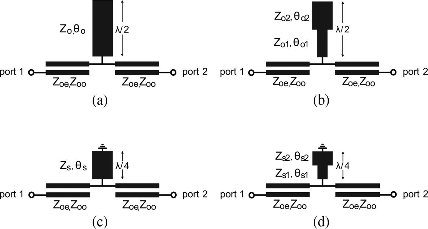
Figure 1 shows four possible single stub-loaded TMRs including the proposed SISS-loaded TMR (in Fig. 1(d)), and the conventional types of TMRs for comparison. Each stub-loaded TMR is composed of the single stub and two coupled-lines where Z oe and Z oo are defined as even-mode and odd-mode impedances of those coupled lines respectively. First, the configuration of the uniform impedance open-circuited stub (UIOS)-loaded TMR is shown in Fig. 1(a), where Z o is the characteristic impedance of the shunt UIOS with the electrical length of θ o (180° at the center frequency f 0). Because of the short circuit condition at 0.5f 0 and 1.5f 0, the shunt open stub resonates and creates transmission zeros at 0.5f 0 and 1.5f 0. Therefore, the UIOS-loaded TMR achieves two transmission zeros at f z1 (=0.5f 0) and f z2 (=1.5f 0) and three resonant frequencies at f m1 (the first resonant frequency), f m2 (the second resonant frequency, f 0), and f m3 (the third resonant frequency) between f z1 and f z2 [Reference Tu12]. Because this TMR cannot be applied to a UWB BPF due to the limited bandwidth (≃ f m3 − f m1), the stepped impedance open-circuited stub (SIOS)-loaded TMR is used to circumvent this problem as shown in Fig. 1(b) where Z o1 and Z o2 are the characteristic impedances of the shunt SIOS with the electrical lengths of θ o1 and θ o2, respectively, for θ o1 + θ o2 = 180° [Reference Singh, Basu and Wang13]. Even though the SIOS-loaded TMR can be used to design a UWB BPF, this TMR has a narrow upper stop-band because it cannot control the parasitic resonance at f m4 (=2f 0), that is, spurious resonance.
Structures of single stub-loaded TMRs: (a) UIOS TMR [Reference Tu12], (b) SIOS TMR [Reference Singh, Basu and Wang13], (c) UISS TMR [Reference Shaman and Hong14], and (d) the proposed TMR.

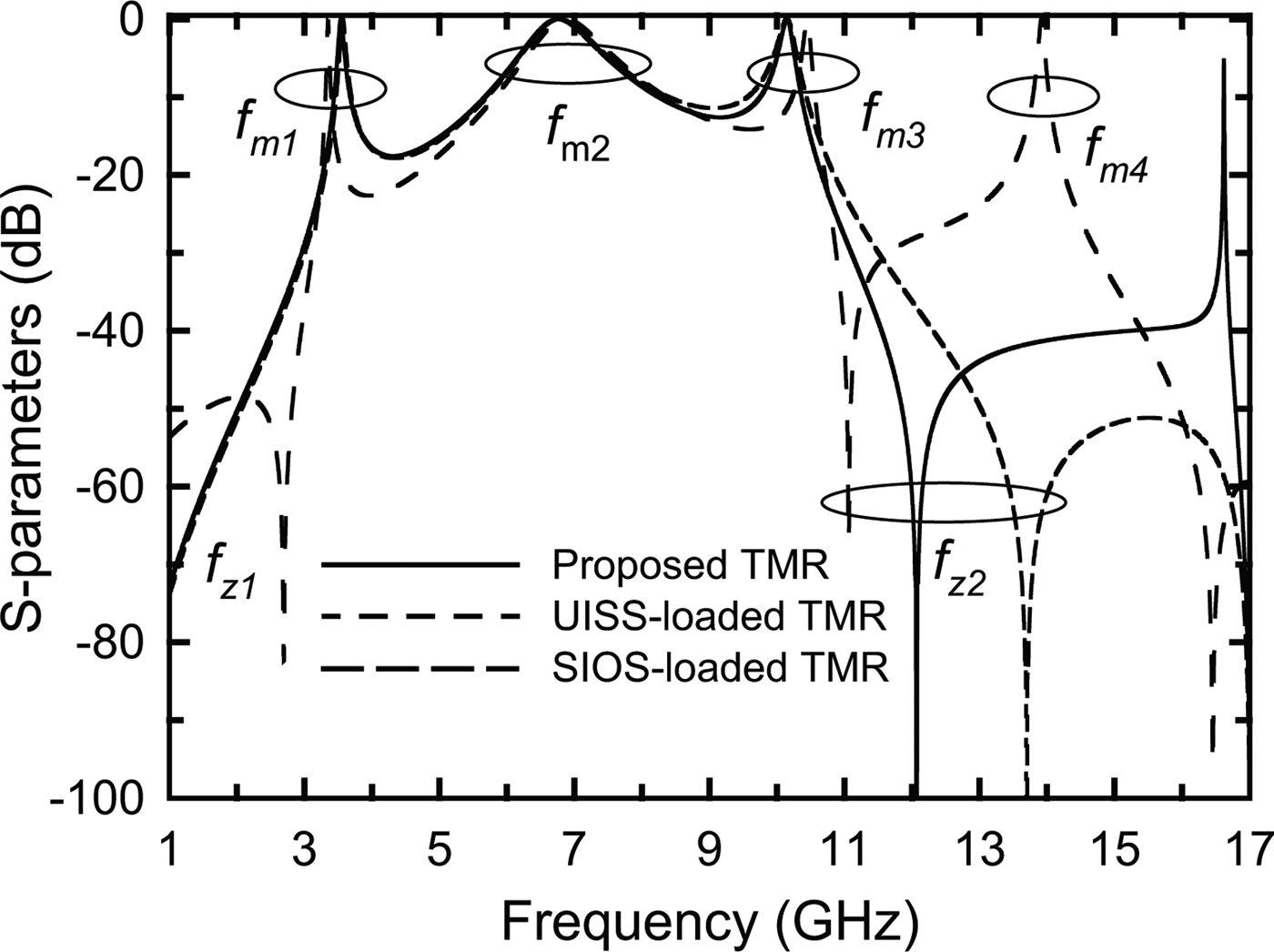
An alternative method, shown in Fig. 1(c), uses a configuration with the uniform impedance short-circuited stub (UISS)-loaded TMR, which has two transmission zeros, f z1 (=DC) and f z2 (=2f 0) and resonances at f m1, f m2, and f m3 [Reference Shaman and Hong14]. Here, Z s is the characteristic impedance of the shunt UISS with electrical length θ s specifically set 90° at f 0. Although this TMR has a wider stop-band than the SIOS-loaded TMR, this structure does not have a sufficiently high selectivity to meet the UWB mask requirements due to the transmission zeros that are not close to the pass-band. To remedy this drawback, the newly proposed SISS-loaded TMR is shown in Fig. 1(d), where Z s1 and Z s2 are the characteristic impedances of the shunt SISS with the electrical lengths of θ s1 and θ s2, respectively, for θ s1 + θ s2 = 90°. Although the electrical properties of the short-circuited stepped impedance resonator were studied for the first time in [Reference Sagawa, Makimoto and Yamashita15], this resonator was employed in a different way than the proposed SISS-loaded TMR. The simulated S 21 response of TMRs with weak coupling is shown to compare the resonant and zero frequencies of these TMRs. As shown in Fig. 2, the proposed SISS-loaded TMR has the merit of a relatively high roll-off ratio at the upper-frequency band edge by shifting f z2 from 2f 0 (=f m4) towards f m3. Therefore, the low selectivity of the UISS-loaded TMR can be increased by the SISS-loaded TMR. A detailed analysis of the proposed SISS-loaded TMR is presented in the following section.
Simulated results of the circuit model for SIOS-, UISS-, and proposed TMR for weak coupling.

Analysis of the proposed SISS
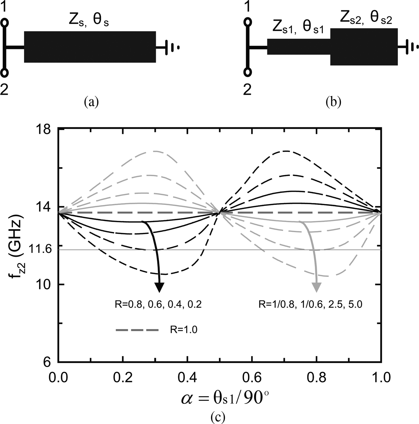
As mentioned above, the second transmission zero f z2 of the proposed TMR in Fig. 2 must be adjusted near the upper pass-band edge to achieve a sharp roll-off ratio. Figure 3 shows a schematic and the variation of f z2 for the UISS and the SISS with different α and R values. The impedance ratio R and electrical length ratio α of the SISS are given, respectively, as
 $$R = Z_{s2}/Z_{s1},$$
 $$\alpha = \theta_{s1}/(\theta_{s1} + \theta_{s2}),$$
where the UISS and SISS have electrical lengths of θ s, θ s1, and θ s2 and these stubs meet θ s = θ s1 + θ s2 = 90° at the center frequency (f c). The UISS and SISS can simultaneously provide transmission zeros at DC (f z1) and other frequencies f zi (i = 2, 3, …) at which their input admittances (or impedances) approach infinity (or zero).
Short-circuited stub structures and characteristics: (a) Circuit model of the UISS, (b) Circuit model of the SISS, and (c) variation of f z2 versus α with different R values of the SISS.

From Fig. 3, the input admittance of the SISS and UISS can be expressed, respectively, as
 $$Y_{\rm SISS} = \displaystyle{{\,j(Z_{s2}\tan\theta_{s1}\tan\theta_{s2} - Z_{s1})} \over {Z_{s1}(Z_{s1}\tan\theta_{s1} + Z_{s2}\tan\theta_{s2})}}, $$
 $$Y_{\rm UISS} = \displaystyle{{1 \over {\,jZ_s\tan\theta_{s}}}}. $$
To create the transmission zeros, in considering the Y SISS and Y UISS to be infinite (i.e., where no transmission occurs in the SISS and UISS), equations (2a) and (2b) can be simplified to
 $$Z_{s1}\tan\theta_{s1}+Z_{s2}\tan\theta_{s2} = 0, $$
 $$Z_s\tan\theta_{s} = 0. $$
For convenience, using the two variables α and R defined in (1a) and (1b), (3a) can be transformed into
 $$\tan(\alpha\theta_{s}) + R\tan\{(1 - \alpha)\theta_{s}\} = 0.$$
Since θ s = 90° at f c, using the relation f z2/f c = 2θ s/π, (4) and (3b) can be expressed as
 $$\tan \left\{\displaystyle{{\pi\alpha} \over {2}} \left(\displaystyle{{\,f_{z2}} \over {\,f_c}} \right)\right\} + R\tan \left\{\displaystyle{{\pi(1 - \alpha)} \over {2}} \left(\displaystyle{{\,f_{z2}} \over {\,f_c}}\right)\right\} = 0, $$
 $${Z_s\tan \left\{\left(\displaystyle{{\pi} \over {2}}\right) \left(\displaystyle{{\,f_{z2}} \over {\,f_c}}\right)\right\} = 0.}$$
According to equations (3a) and (3b), the UISS is a special case of the SISS with R = 1 for any value of α. Although the second transmission zero (f z2) of the UISS in (5b) is always 2f c (f z1 = DC) and not controllable, that of the SISS can be controlled by different values of R and α (Z s1, Z s2, θ s1, and θ s2).
To illustrate (5a) due to its complicated form, the variation of f z2 versus α for different R values is presented in Fig. 3(c), where f c values of these stubs are designated to be 6.85 GHz. The dark, light, and long-dash gray lines in this figure indicate R < 1, R > 1, and R = 1, respectively. While f z2 of the UISS (R = 1) is fixed at 13.7 GHz, that of the SISS is variable for many cases of 0<R < 1 and 0 < α < 1 except for three locations, namely, α = 0, 0.5, and 1. Therefore, we have confirmed that the f z2 of the SISS can be freely adjusted, excluding the cases in which α = 0.5. Clearly, in Fig. 3(c), the graph is symmetrical around the point α = 0.5 and f z2 = 2f c = 13.7 GHz, which includes the condition R = 1. In the next subsection, this stub will be used to design the proposed SISS-loaded TMR.
Resonance properties of the SISS-loaded TMR
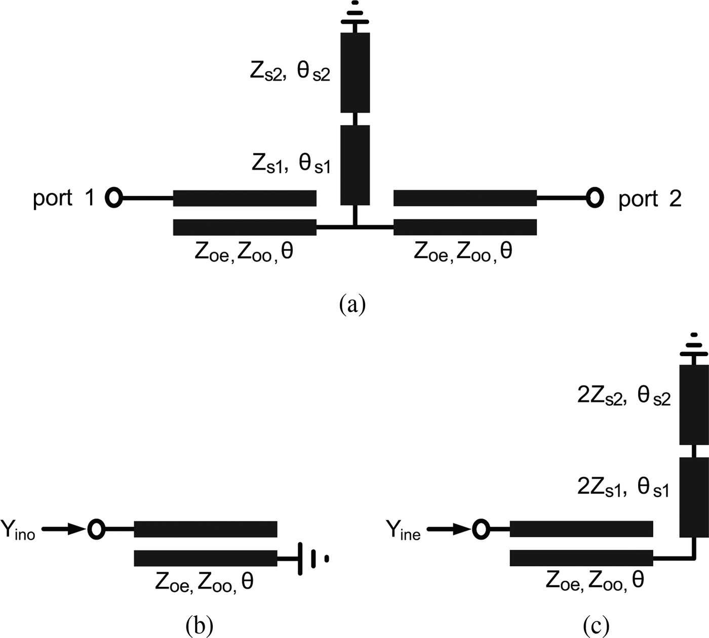
Figure 4(a) presents a schematic of the SISS-loaded TMR. This resonator is composed of the SISS and feeding coupled lines. Because this TMR is symmetrical in structure, even- and odd-mode analysis is performed.
The proposed TMR: (a) overall structure, (b) odd-mode equivalent circuit, and (c) even-mode equivalent circuit.

For odd-mode excitation, the equivalent circuit shown in Fig. 4(b) is used. The odd-mode input admittance Y ino can be expressed as
 $$ Y_{ino} = {\displaystyle{{\,j(Z_{oe}+Z_{oo})\sin(2\theta)} \over {(Z_{oe}+Z_{oo})^{2}\cos^{2}\theta-(Z_{oe}-Z_{oo})^{2}}}}. $$
From the resonance condition of Y ino = 0, the odd-mode resonant frequency f om is determined by
 $$f_{om} = f_c. $$
It can be found that the odd-mode resonant frequency is located at f c with θ = 90° and is not affected by the use of the SISS.
For even-mode excitation, the equivalent circuit in Fig. 4(c) is used. The even-mode input admittance Y ine can be written as
 $$Y_{ine} = {\displaystyle{{Y_{\rm SISS}A\sin(2\theta) + 4j\sin^{2}\theta} \over {A\sin(2\theta)+jY_{\rm SISS}(B^{2} - A^{2}\cos^{2}\theta)}}}, $$
 $$A =(Z_{oe}+Z_{oo}), $$
 $$B =(Z_{oe}-Z_{oo}). $$
From the resonance condition of Y ine = 0, the even-mode resonant frequencies f em1 and f em2 can be obtained after solving (8a) using the relation of f em1;2/f c = 2θ s/π = 2θ/π.
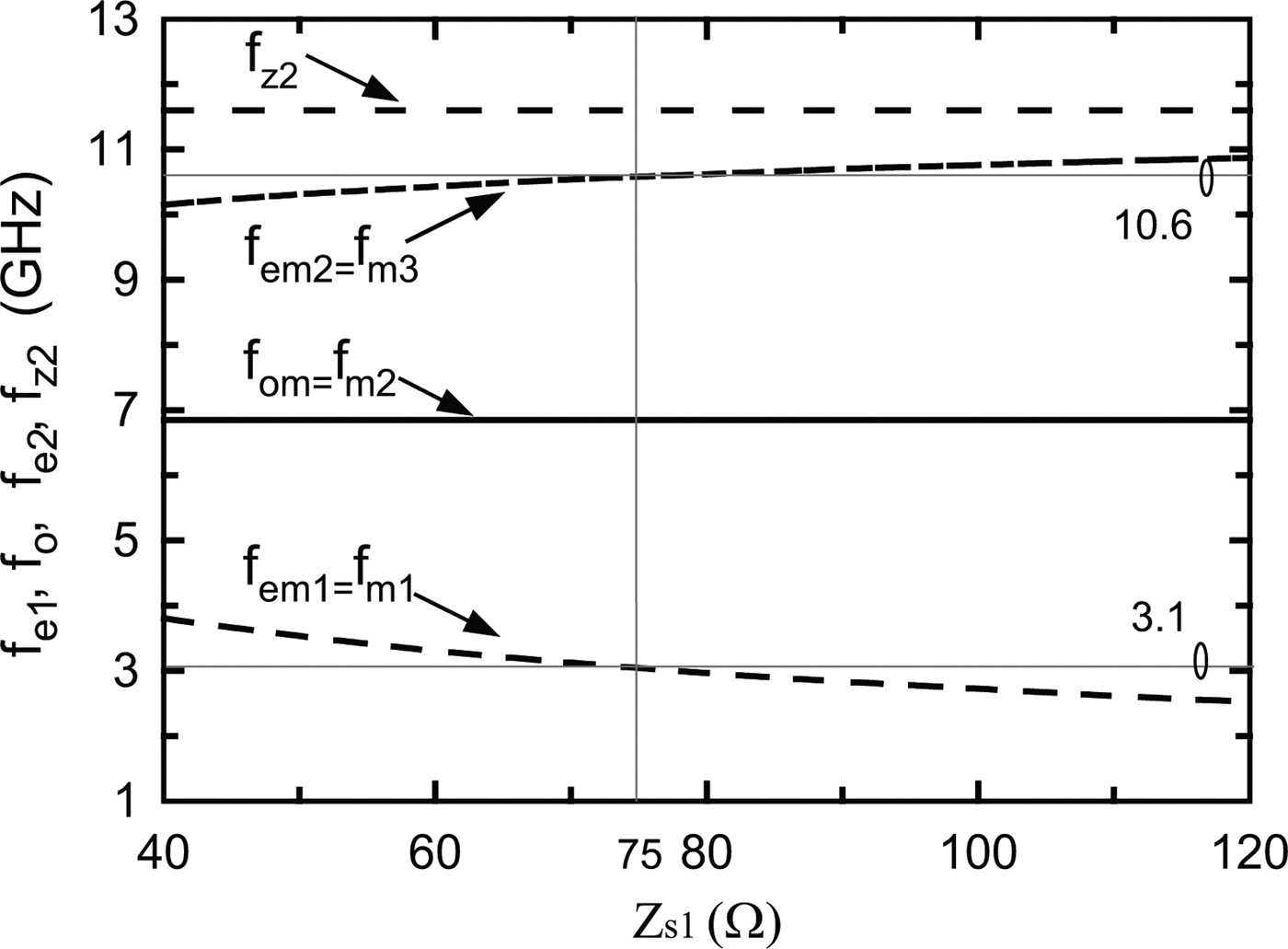
Because of its complicated mathematical form, circuit simulation is carried out using Advanced Design System (ADS) to verify the above equations for the resonant mode frequencies and the second transmission zero. It can be shown in (8a)–(8b) that the even-mode resonant frequencies can be altered by adjusting the values of Z oe and Z oo of the coupled feed lines and the values of Z s1, R, and α of the SISS. Choosing the values of α = 0.26 and R = 0.4 given in Fig. 3(c) to set f z2 at 11.6 GHz, the variation of operating resonant frequencies and second transmission zero versus Z s1 is plotted in Fig. 5, where the coupling factor of the coupled feed lines is set to create weak coupling. Because of the dependence of Z s2 on Z s1 at a fixed value of R, this figure uses Z s1 as its lateral axis. This figure shows that the odd-mode resonant frequency f om is not affected by the value of Z s1, as is expected. On the other hand, the even-mode resonant frequencies, f em1 and f em2, decrease and increase, respectively, as Z s1 increases. Unlike the UISS-loaded TMR for the case of R = 1, the proposed TMR can control the second transmission zero as well as the even-mode resonant frequencies.
Variation of operating resonant frequencies and second transmission zero versus Z s1 for α = 0.26 and R = 0.4.

It is noteworthy that the SISS-loaded TMR's bandwidth with the return loss lower than − 20 dB will be significantly increased by a high coupling factor of the parallel-coupled lines [Reference Li and Zhu16, Reference Wong and Zhu17]. Thus, to overcome the limited coupling factor of the two-line coupled schemes, three-line coupled schemes are adopted to enhance the coupling factor, as described in the next section.
Implementation and comparison
As described above, the desired R and α values of the SISS for a given f z2 are selected based on equations (5a) and (5b) and Fig. 3(c). Because of the parasitic effects of discontinuities at the junction, the width of the SISS connected to the three-line coupled scheme should be narrower than the width to be shorted. Therefore, the SISS for R < 1 (Z s1 > Z s2) is used to design the proposed UWB BPF. For the SISS with R < 1, the values of α = 0.26 and R = 0.4 at which f z2 was found for 11.6 GHz [indicated by a thin horizontally line in Fig. 3(c)] are selected so as to maximize R (to the nearest unit value), resulting in a small junction width.
After we determine f z2 at 11.6 GHz with α = 0.26 and R = 0.4, the first three resonant frequencies can be also set based on Fig. 5. For the specially fixed value of Z s1 (vertically marked by a thin line) for α = 0.26 and R = 0.4, f em1, f om, and f em2 are generated at 3.1, 6.85, and 10.6 GHz, respectively. Therefore, the design parameters of the proposed SISS such as Z s1, Z s2, θ s1, and θ s2 are equal to 75 Ω, 35 Ω, 23°, and 67°, respectively.
To determine the bandwidth of the coupled line for a UWB BPF design, the image impedance Z i method in [Reference Pozar18] is used. Z i is given by
 $$Z_i = \sqrt{(Z_{oe} - Z_{oo})^{2}{\rm csc}^{2}\theta - (Z_{oe} + Z_{oo})^{2}\cot^{2}\theta}. $$
When the coupled line section is λ/4 at f c, which is the center frequency of the UWB BPF, the image impedance reduces to
 $$Z_i = (Z_{oe} - Z_{oo})/2, $$
and the electrical lengths (θ f and θ e) at the roll-off frequencies of the coupled line can be found as
 $$\cos \theta_f = -\cos\theta_e = \left(\displaystyle{{Z_{oe}} \over {Z_{oo}}} -1 \right) / \left(\displaystyle{{Z_{oe}} \over {Z_{oo}}} + 1\right), $$
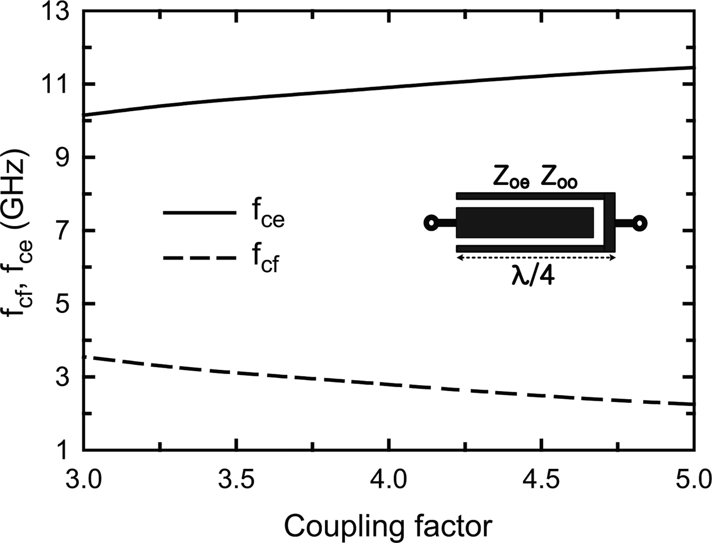
where θ e = π − θ f. Figure 6 presents f cf and f ce of the coupled line versus the coupling factor, defined as Z oe/Z oo, where f cf and f ce are the front and end roll-off frequencies. The bandwidth (f ce − f cf) of the coupled line is broaden when its coupling factor increases where the bandwidth is defined for −20-dB return loss (Z i = 55Ω). To determine the 3-dB bandwidth of 116%, (10) and (11) are modified as follows:
 $$Z_{oo} = Z_{oe} - 110, $$
 $$Z_{oe} = 3.7 \times Z_{oo}. $$
Based on (12a) and (12b), the coupled line even- and odd-mode impedances are selected for Z oe = 150 Ω and Z oo = 40 Ω. With a coupling factor of 3.7 in Fig. 6, f cf and f ce are chosen to be 2.95 GHz and 10.75 GHz, respectively. The physical dimensions of the coupled line can be found with electromagnetic simulations.
Simulated f cf and f ce values for three-line coupled scheme versus the coupling factor with −20-dB return loss at f o.

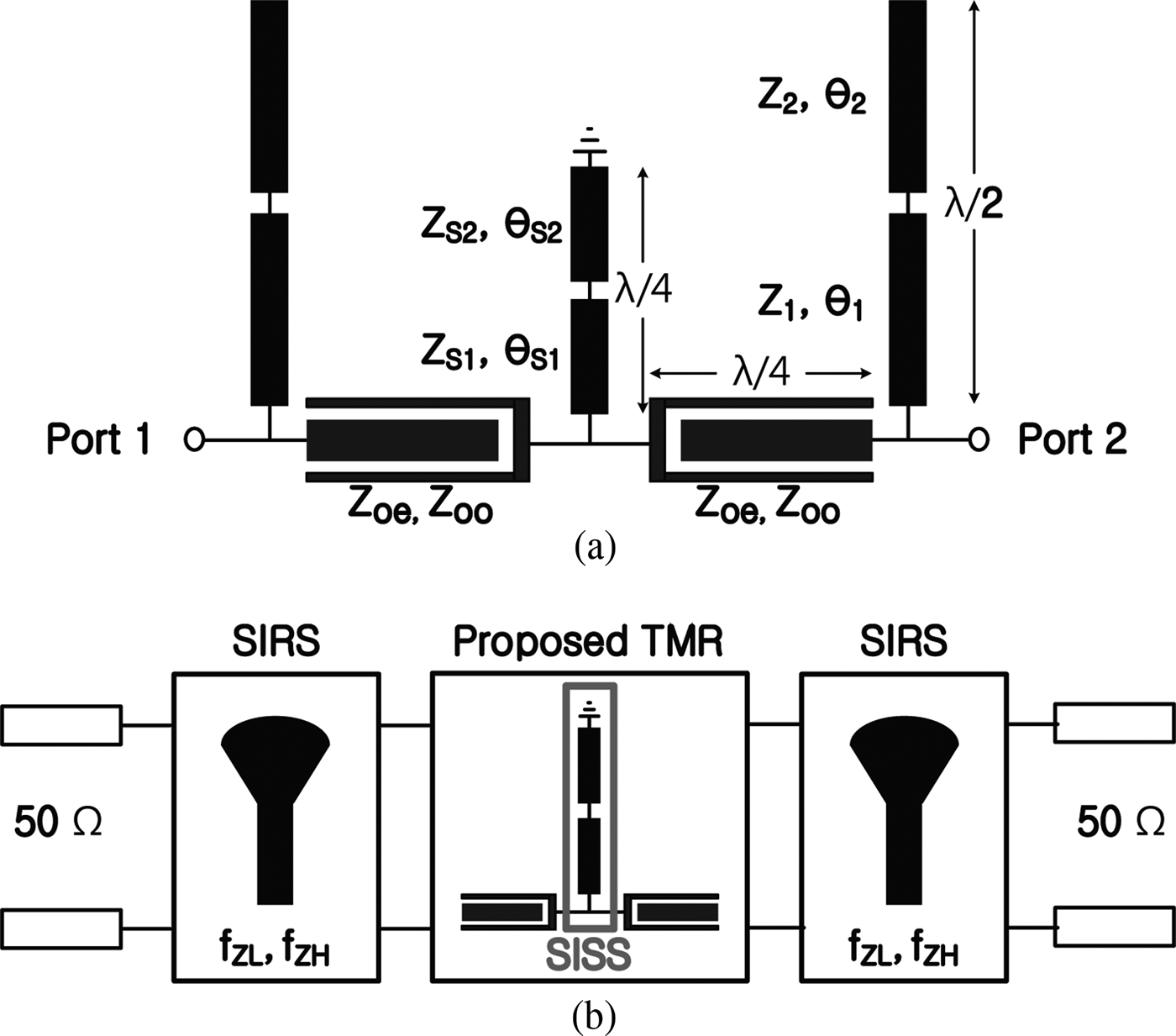
To further improve the roll-off ratio at the lower and upper passband edges and the impedance matching in the UWB pass-band, the λ/2 SIOS with impedances of Z 1 and Z 2 (shown in Fig. 7) is introduced in order to provide additional transmission zeros. The input impedance of the SIOS is expressed by
 $$Z_{SIOS} = \displaystyle{{\,jZ_1(Z_1\tan\theta_1 - Z_2\cot\theta_2)} \over {Z_1 + Z_2\tan\theta_1\cot\theta_2}}. $$
The proposed UWB BPF: (a) schematic and (b) equivalent model.

To create the transmission zeros,
 $$Z_1 \tan \theta_{1} - Z_{2} \cot \theta_{2} = 0. $$
Assuming θ 1 = θ 2 = θ s (= π/4 at f c) and defining Z 2/Z 1 = K and 2θ s/π = f z/f s, (14) can be solved as
 $$\theta_s = \tan^{-1}\sqrt{K}$$
 $$f_{zL} = \displaystyle{{2f_s} \over {\pi}}(\tan^{-1}\sqrt{K}),$$
 $$f_{zH} = \displaystyle{{2f_s} \over {\pi}} (\pi-\tan^{-1}\sqrt{K})$$
where f s, f zL, and f zH are the center, lower transmission zero, and upper transmission zero frequencies, respectively. Specifically, the upper transmission zero of SIOS must be located at the same frequency as that of the SISS (f z2). To design a highly selective UWB BPF, Z 1 = 130Ω and Z 2 = 35Ω (K=0.27), and f s = 6.85 GHz are chosen to give f zL and f zH values of 2.0 GHz and 11.6 GHz, respectively. The schematic and equivalent model of the proposed UWB BPF are shown in Fig. 7.
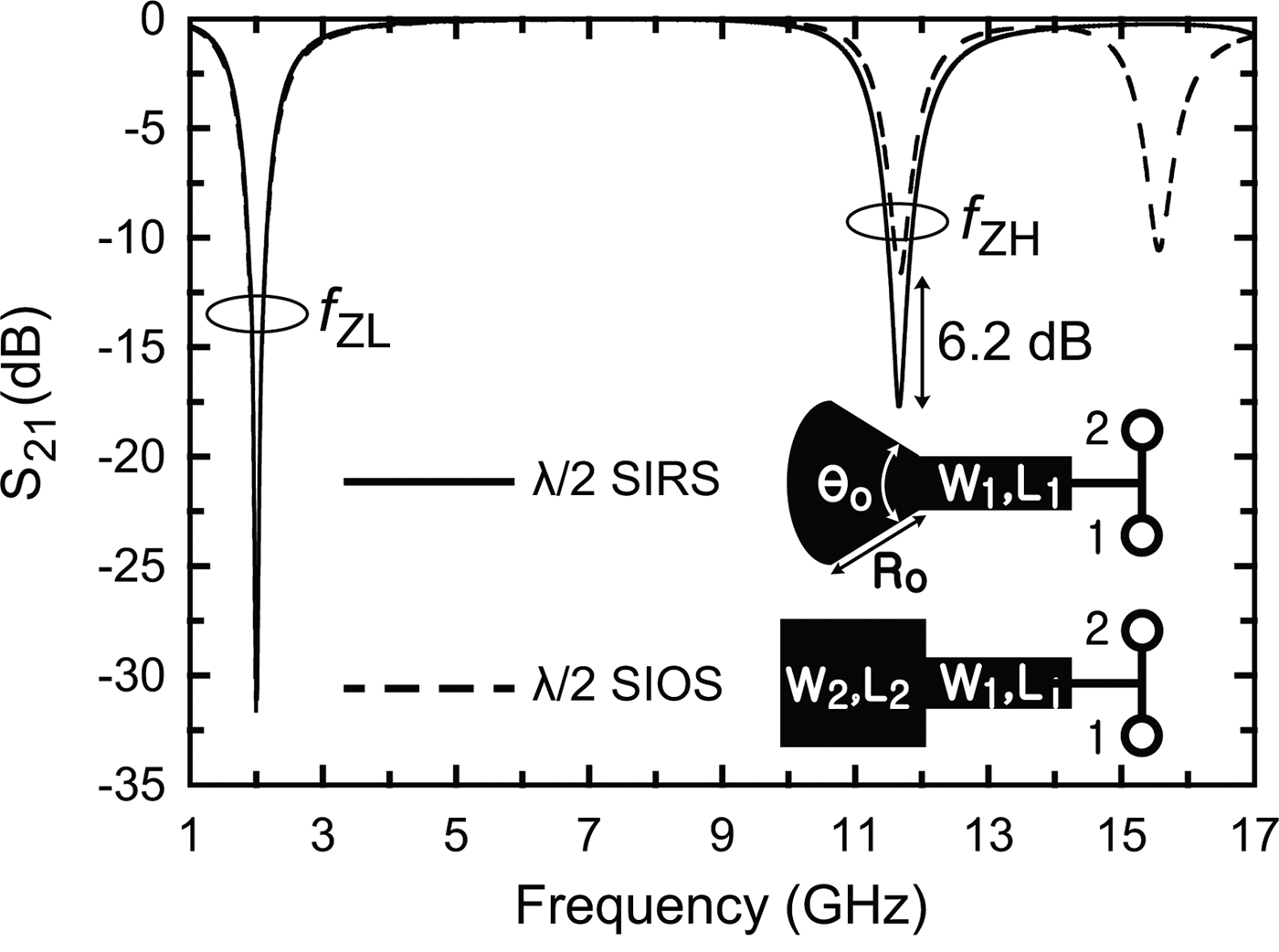
However, the parasitic dissipation effect on the λ/2 SIOS shown in Fig. 7 especially steps in width between the two transmission lines, significantly reduces the rejection level of this stub or quality factor of this stub, especially at f zH. Such parasitic dissipation can lead to substantial differences between the realized and ideal SIOS response. To overcome this drawback, the stepped impedance radial stub (SIRS) is adopted in the proposed UWB BPF to have a high-quality factor at f zH. Figure 8 shows the S-parameter response of the conventional SIOS and proposed SIRS for comparison. W 1, W 2, L 1, and L 2 are the physical parameters of the conventional SIOS, W 1, L 1, r o, and θ o are those of the proposed SIRS for electrical parameters Z 1, Z 2, θ 1, θ 2, respectively where r o and θ o are the radius and center angle of the proposed SIRS. The values of r o and θ o are obtained based on the following equation:
 $$\displaystyle{{1} \over{2}}(r_o \times \theta_o) = W_2. $$
As a result, the maximum stop-band attenuation at f zH has been improved from 11.5 to 17.7 dB by the difference of 6.2 dB, as shown in Fig. 8. Thus it can be shown that the proposed SIRS has a higher quality factor than the conventional one which improves the rejection of the proposed UWB BPF at f zH by the difference of 6 dB.
Schematic and transmission attenuation of λ/2 SIRS and SIOS.

Experimental verification
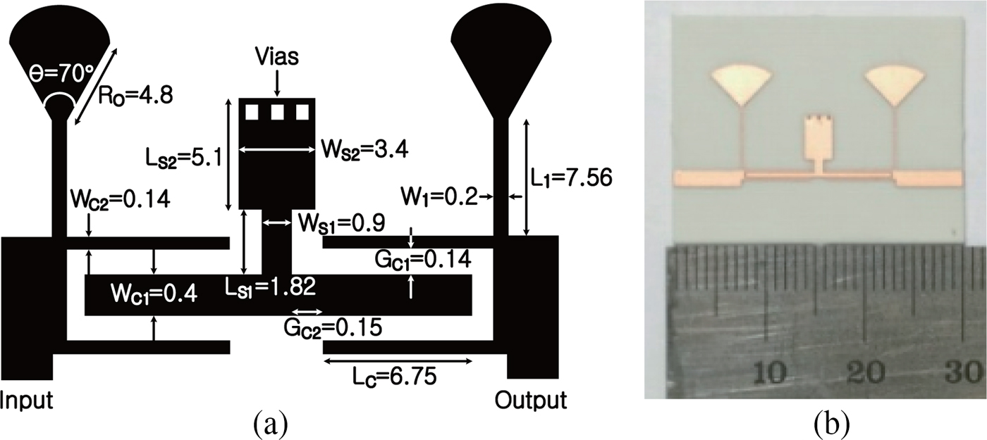
The final layout and photograph of the proposed UWB BPF is shown in Fig. 9. The proposed UWB BPF has a compact circuit size of 30 mm × 18 mm (i.e., 0.55λ g × 0.47λ g, where λ g is the guided wavelength of the microstrip structure at 6.85 GHz) including the 50-Ω microstrip feeding lines. The proposed UWB BPF is fabricated on a Rogers RO4003C substrate with the thickness of 0.81 mm, the relative dielectric constant of 3.38, and tanδ = 0.0027 and measured using an Anritsu 37247D vector network analyzer (VNA), and a test fixture with the line-reflect-line (LRL) calibration.
The proposed UWB BPF: (a) layout and (b) photograph.

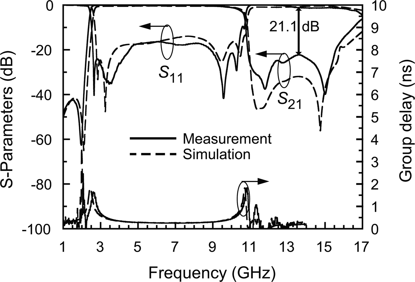
The simulated and measured results are also demonstrated in Fig. 10, where good agreement between simulation and measurement is shown. The measured center frequency is 6.6 GHz and the 3-dB bandwidth is 121% from 2.5 to 10.6 GHz. Moreover, the fabricated BPF has a minimum insertion loss less than 0.17 dB at 6.85 GHz and a return loss better than 16 dB within the pass-band. Figure 10 reveals that this BPF exhibits sharp roll-off at the lower and upper edge with slopes of 96 and 43 dB/GHz, respectively. Furthermore, high rejection levels are achieved at the lower stop-band up to 2.26 GHz and upper stop-band from 10.8 to 15.6 GHz with greater than 20-dB level of suppression which value is designated as the FCC-defined UWB hand-held limit in the out-of-band. The measured group delay with a variation of 0.69 ns is also shown in this figure. In Fig. 10, it can be questionable why there are two transmission zeros in the upper band. One is located at 11.6 GHz and the other at 15 GHz. The first one is generated by the SISS which can be explained by equations (5a), (5b) and (15c) and the second one by the transmission zero of the coupled feed line. Although the center frequency of the coupled line is at 6.85 GHz, due to the difference in the even/odd phase velocities of the coupled line, transmission zero is not generated at 13.7 GHz but at 15 GHz.
Measured and simulated results of the UWB BPF.

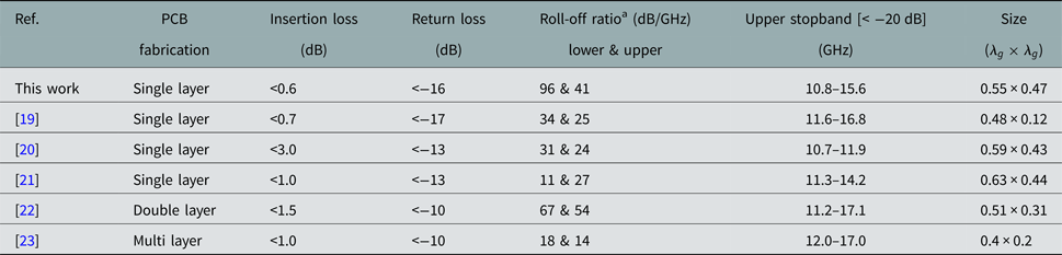
Table 1 shows a comparison of the proposed UWB BPF with other previously reported UWB BPFs. The proposed UWB BPF requires single-layer microstrip fabrication and has an excellent in-band performance such as small insertion and return losses. Moreover, the designed UWB BPF has good out-of-band performance with a higher roll-off ratio and a wider stop-band, relative to other works. The proposed UWB BPF's simple design procedures can be adjusted to apply it to other wide frequency bands.
Comparison of several UWB BPFs

a The roll-off ratio is defined as 27/(|f 3dB − f 30dB|) where f 3dB is the 3-dB roll-off frequency and f 30dB is the 30-dB table_example stopband frequency.
Conclusion
A highly selective UWB BPF has been implemented and carefully analyzed. By introducing a SISS to the TMR and adopting a SIRS, the lower and upper transmission zeros were generated and properly located so as to enhance the roll-off ratio, especially at the upper frequency edge. The measured results show good agreement with the simulated results. Excellent in-band characteristics including low insertion losses and good out-of-band performance (including high selectivity and a wide stop-band with spurious rejection above 20 dB from 10.8 to 15.6 GHz) are attained for a single-resonator-based BPF fabricated using a microstrip process. Therefore this filter is attractive for the IOT application of the UWB technology.
Acknowledgments
This work was supported by Space Core Technology Program through the National Research Foundation of Korea funded by the Ministry of Science and ICT (NRF-2017M1A3A3A02016255).
 Minjae Jung was born in Daegu, Korea. He received a B.S. degree in electrical and electronics engineering from Chung-Ang University, Seoul, Korea, in 2013, and is currently working toward a Ph.D. degree at Yonsei University, Seoul, Korea. His research interests include wideband/tunable microwave filters for cognitive-radio communication systems and millimeter wave ICs for phased-array antenna applications.
 Byung-Wook Min was born in Seoul, Korea. He received the B.S. degree from Seoul National University, Seoul, Korea, in 2002, and the M.S. and Ph.D. degrees from The University of Michigan at Ann Arbor, in 2004 and 2007, respectively. During 2006–2007, he was a Visiting Scholar with the University of California at San Diego, La Jolla. He is currently an Associate Professor with the Department of Electrical and Electronic Engineering, Yonsei University, Seoul, Korea. During 2008–2010, he was a senior engineer at Qualcomm Inc., Santa Clara, CA and Austin, TX. His research interests include Si/SiGe RFIC and communication systems for microwave and millimeter-wave applications.