I. INTRODUCTION
An important component of any wideband system is the pulse generator (PG). An ultra-wideband (UWB) signal is defined by its bandwidth (>500 MHz) and limitations on the power-spectrum of UWB pulse shapes were imposed by FCC's reform in 2002 [1, Reference Badamchi, Valizade, Rezaei and Badamchi2]. The step, Gaussian, monocycle, and polycycle are the most commonly used pulse shapes for wideband systems. Although each of these pulse shapes has its unique merits, the monocycle is the most commonly used due to its simpler realization, wide spectrum, and more importantly because it does not contain low frequency spectrum including DC and therefore it can be transmitted through a practical antenna [Reference Han and Nguyen3, Reference Han and Nguyen4].
Various techniques for short pulse generation have been proposed involving different impulse-like PG devices such as MESFET, step recovery diode (SRD), avalanche diode, and gallium arsenide photoconductive switches [Reference Maxwell, Weller and Odu5]. However, due to the increasing demand for low-power consuming handheld wideband devices it is desirable to have compact low cost PGs and other integrated RF modules [Reference Maxwell, Weller and Odu5–Reference Valizade, Rezaei and Orouji7]. The SRDs are the most promising devices for low power sub-nanosecond pulse generation. The SRD works as a charge controlled switch and its ability to change very rapidly from low impedance to a high impedance state can be used to sharpen the slow waveform edges. Transition time (T t ) and minority carrier life time (MCLT) are the most important characteristics of the SRD. The transition time of the SRD determines the minimum achievable pulse's transition time while the MCLT affects the storage time under reverse bias condition [Reference Han and Nguyen4]. Moreover, many existing wideband PGs are capable of producing only a single type of pulse. However, modern wideband systems require transmitters with tuneable pulse width or multiple pulse shape generation capability. In addition multiple pulse shape generation can provide pulse shape modulation, which is desirable for encoding data in communication systems [Reference Mirshafiei, Abtahi and Rusch8–Reference Ghavami, Michael, Haruyama and Kohno10].
In this paper a novel design of reconfigurable wideband PG is presented. The designed PG output signal is able to switch between Gaussian and monocycle pulse shapes. The employed pulse shaping circuit consists of an RC differentiator, which can be effectively bypassed by a PIN diode leading to two different pulse shapes at the output port. Moreover, unlike many recently published wideband PGs, which employ input driving clock pulses with fast rise/fall times (few nanoseconds) [Reference Han and Nguyen3, Reference Han and Nguyen4], the presented PG in this paper is driven by a 10 MHz sinusoidal signal. In the next sections the design procedure and the structure of the proposed reconfigurable wideband PG is illustrated in details.
II. DESIGN AND CONFIGURATION
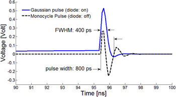
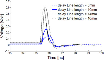
The proposed reconfigurable SRD-based PG schematic is shown in Fig. 1, which consists of a Gaussian PG, a pulse shape selector, and the load section. The Gaussian PG section generates sharp pulses from a 10 MHz sinusoidal input signal using an SRD and a shunt short circuited transmission line (delay line). The input signal driving the series SRD creates a step-like pulse, which further divides into two equal pulses travelling toward the short circuited stub and pulse shape selector section. The reflected signal from the short circuit is 180° out of phase and combines with the next incident step-like pulse at the SRD-transmission line junction forming a sharp Gaussian pulse [Reference Kamal, Bhattacharya, Tamrakar and Roy11]. The length of the short circuited stub is L d = τV p /2, in which τ is the pulse duration, and V p is the speed of the wave. Other parameters especially the physical characteristics of the employed SRD such as the carrier life time of the SRD should also be considered during selection of the delay line length [Reference Chan, Rambabu, Tan and Chia12]. Agilent advanced design system simulation software (Agilent ADS) was used as the simulator [13] and the generated Gaussian pulse at the SRD-transmission line junction is shown in Fig. 2. A tuning practice has been performed during simulation in order to obtain the final value for the delay line length and the simulated results are depicted in Fig. 3. According to this figure, shorter stub can create shorter pulse duration but this will reduce the pulse amplitude significantly.
The schematic of the proposed reconfigurable wideband PG.

Simulated output pulse shapes of the proposed PG.

The various simulated output Gaussian pulses with the delay line length as a parameter.

Same technique can be used in order to create monocycle pulse shape by combining two Gaussian pulses having 180° phase difference and certain time delay between them. However, the produced monocycle pulse will have a pulse duration about twice of that of the original Gaussian pulses [Reference Chan, Rambabu, Tan and Chia12]. Therefore in order to avoid pulse duration degradation, a first order RC differentiator (high pass filter) is employed to generate monocycle pulse shape. The RC differentiator consists of the load impedance R L and the capacitance C D , as shown in Fig. 1. The coupling capacitances named C C in Fig. 1 are chosen very larger than the C D and thus they can be ignored during differentiator calculations.
Assuming a Gaussian pulse, which is expressed as equation (1) in which A is the amplitude of the Gaussian pulse, f c is the center frequency, and t is time, taking derivative of equation (1) gives the monocycle pulse shape as equation (2). Having f c = 1/2πR L C, by choosing the desirable frequency band of 0.5–1.5 GHz and R L = 50, the C D can be calculated in range of 2–3 pF.
 $$V{\rm (}A,t,f_c {\rm )} = Ae^{ - 2{\rm (}\pi f_c t{\rm )}^2},$$
 $$V{\rm (}A,t,f_c {\rm )} = 2\sqrt e A\pi tf_c e^{ - 2{\rm (}\pi f_c t{\rm )}^2}.$$
In order to create a reconfigurable PG with pulse shape modulation (PSM) capability, a PIN diode is embedded parallel with the C D as shown in Fig. 1. The PIN diode acts as a low impedance (usually 2–5 Ω) at its on state and thereby the C D is bypassed and the effect of the differentiator is canceled and the output signal has a Gaussian shape. On the other hand, when the PIN diode is off it can be considered as a small capacitance (C P < 1 pF), which is equal to a large impedance at high frequencies and therefore the effective capacitance of the differentiator becomes C eff = C D + C P and the output signal has a monocycle shape. After inserting the PIN diode a tuning process is done in order to obtain the final values of employed components. The final values of the components in Fig. 1 are: R S = R L = 50 Ω, C D = 2.2 pF, C C = 100 nF, transmission line length = 14 mm, V bias = 2 V, PIN diode junction capacitance = 0.33 pF, and PIN diode forward resistance = 1 Ω. The SRD is assumed to have carrier life time of 50 ns, transition time of 120 ps and junction capacitance of 3 pF. The simulation results reveal that the generated Gaussian and monocycle pulses have 700 and 800 ps pulse widths, respectively and the full-width-at-half-maximum (FWHM) for the Gaussian pulse is 400 ps.
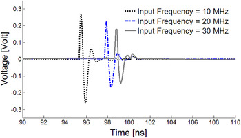
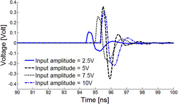
Moreover, various simulation studies have been performed in order to examine the robustness of the presented reconfigurable PG against any changes in the input signal alteration. Various simulated output monocycle pulses with the input excitation signal frequency as a parameter are depicted in Fig. 4. As can be observed in this figure although the amplitude of the output pulses are decreased by changes in the excitation frequency, the monocycle pulse shape characteristic of the output pulse is well preserved, which is desirable. Also, various simulated output monocycle pulses with the input excitation signal amplitude as a parameter are depicted in Fig. 5. As can be observed in this figure, both amplitude and pulse width of the output pulse are influenced by the amplitude of the input excitation signal. However, the output monocycle pulse shape is again well preserved, which is a desirable characteristic in most applications with PSM [Reference Ghavami, Michael, Haruyama and Kohno10].
The various simulated output monocycle pulses with the input excitation signal frequency as a parameter.

The various simulated output monocycle pulses with the input excitation signal amplitude as a parameter.

III. RESULTS AND DISCUSSION
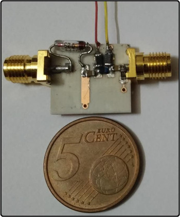
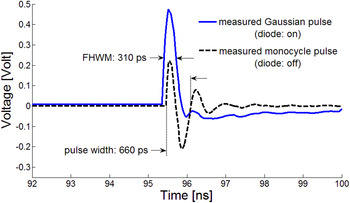
A prototype of the proposed reconfigurable wideband PG is realized on a RO4003 substrate (ε r = 3.38, h = 0.8 mm) and its photograph is shown in Fig. 6. The employed SRD and PIN diode are HP 5082-0112 and BAR64-03W, respectively. As can be observed in Fig. 6 the components in the fabricated PG are tightly soldered together in order to avoid any unwanted performance alteration due to the distributed microstrip transmission lines effects [Reference Singama, Burk and Piette14, Reference Xia, Venkatachalam and Huston15]. A pair of wires is used in order to apply the DC bias to the embedded PIN diode. Figure 7 shows the measured output signals for different biasing conditions of the PIN diode when it was driven by a 10 MHz 5 V p sinusoidal signal. As can be observed in Fig. 7 the measured Gaussian waveform has 510 ps pulse duration, amplitude of 470 mV, and FWHM of 310 ps. The ringing level for the measured Gaussian pulse is −24.85 dB. Moreover, the measured monocycle pulse has pulse duration of 660 ps, 430 mV peak-to-peak amplitude, and ringing level of −11.5 dB. Good symmetry for both amplitude and shape exists between the positive and negative portions of the generated monocycle pulse. Although, comparing the simulation results in Fig. 2 with the measured results in Fig. 7 shows that the fabricated PG has a better performance in case of pulse width, it should be noted that another important issue which must be considered is the damping time of the ringing effect, which is longer for the measured results. This could be due to a number of parameters such as the manufacturing accuracy, SMA connectors, and the soldering process. However, in an overall point of view fine agreement exists between the simulated and measured results.
The photograph of the realized reconfigurable PG.

The measured output pulse shapes for various biasing states of the embedded PIN diode.

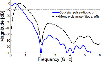
Moreover, the frequency bandwidth of the generated Gaussian and monocycle pulses have also been calculated using fast Fourier transform and the obtained results are shown in Fig. 8. The available bandwidth (>−10 dB) for both Gaussian and monocycle pulses are more than 500 MHz and therefore the proposed reconfigurable PG can be categorized as UWB PG.
Calculated power spectrum of the measured Gaussian and monocycle pulses generated by the designed reconfigurable pulse generator.

A comparison between the proposed reconfigurable wideband PG with other similar PGs, which are recently published in the literature is presented in Table 1. According to this table the proposed reconfigurable PG structure has suitable performance and can be a good candidate for various wideband applications.
Comparison of this work with other pulse generators.

IV. CONCLUSION
A novel compact reconfigurable UWB SRD PG with switchable pulse shaping performance has been designed, fabricated, and tested. A simple RC high-pass filter was used to directly generate the monocycle pulse from the sharpened Gaussian pulse. Only a single PIN diode is employed to create the switchable reconfigurable performance. The simplicity, low cost, and good performance of this circuit makes it attractive for various low rate UWB systems with pulse shape modulation.
ACKNOWLEDGEMENTS
The authors thank the Dynamic Microwave Electronics (DMWE) company staff for their professional help and support. (http://www.dmw-electronics.com)
 Arash Valizade was born in Tehran, Iran 1986. He received his B.Sc. degree in Electrical Engineering-Electronics from Azad University of Sabzevar, Iran, in 2008 and M.Sc. degree in Electrical Engineering-Telecommunication from Urmia University, Urmia, Iran, in 2012, and Ph.D. degree in Electrical Engineering–Telecommunication from Semnan University, Semnan, Iran in 2016. His primary research interests are in numerical methods in electromagnetics, microstrip antenna design, microwave circuits, active integrated antenna design, and reconfigurable structures.
 Pejman Rezaei was born in Tehran, Iran, in 1977. He received the B.S. degree in Electrical Engineering from Communication Faculty, Tehran, Iran, in 2000, and the M.S. and Ph.D. degrees from Tarbiat Modarres University, Tehran, Iran, in 2002 and 2007, respectively. Currently, he is associate professor in the Semnan University, Semnan, Iran. His current research interests are electromagnetics theory, antenna theory and design, reconfigurable antenna.
 Ali Asghar Orouji was born in Neyshabour, Iran in 1966. He received the B.S. and M.S. degrees in Electronic Engineering from the Iran University of Science and Technology (IUST) Tehran, Iran in 1989 and 1992, respectively. Then, he received the Ph.D. degree from the Indian Institute of Technology, Delhi, India in 2006. Since 1992, he has been working at the Semnan University, Semnan, Iran as a faculty member. His research interests are in modeling of SOI MOSFETs, novel device structures, and theory and design of antenna, and wave propagation.