Introduction
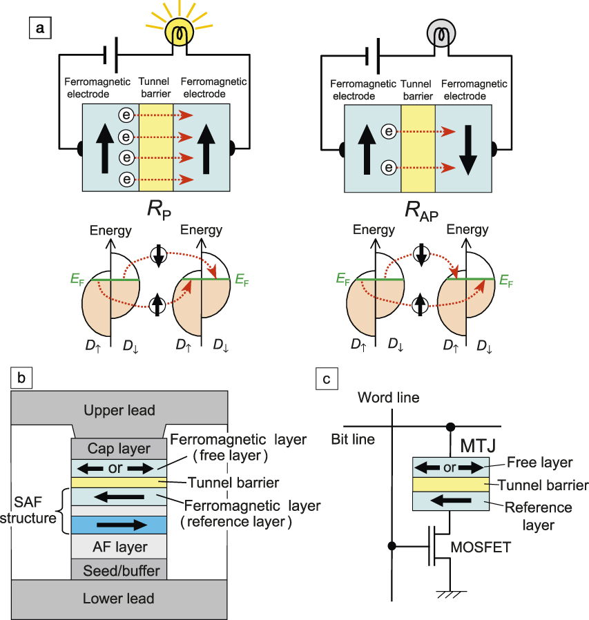
A magnetic tunnel junction (MTJ), which consists of an ultrathin insulating layer (a tunnel barrier) sandwiched between two ferromagnetic metal layers (electrodes), shows a magnetoresistance effect. As illustrated in Figure 1a, the tunneling resistance of an MTJ depends on the relative magnetic alignment (parallel or antiparallel) of the ferromagnetic electrodes. Usually, the resistance for the parallel magnetic state, R P, (Figure 1a [left]) is lower than that for the antiparallel state, R AP (Figure 1a [right]). This phenomenon, called the tunnel magnetoresistance (TMR) effect, is the core technology in several spintronic devices. The size of the TMR effect is measured by the fractional difference in resistance, (R AP – R P)/R P × 100 (%), which is called the magnetoresistance (MR) ratio. The TMR effect originates from spin-dependent electron tunneling between the ferromagnetic electrodes. The MR ratio of MTJs can be phenomenologically expressed as:
 $$MR\, = \,{{2{P_1}{P_2}} / {(1 - {P_1}{P_2}}}),$$
where P 1 and P 2 are the spin polarizations of tunneling electrons at the Fermi energy (E F) of the two electrodes. Because the density of states (DOS) in ferromagnets is spin-polarized at E F, the tunneling resistance changes depending on the relative magnetic alignment.Reference Julliere1
(a) Schematic illustrations of the tunnel magnetoresistance effect in a magnetic tunnel junction (MTJ) (left panels: parallel magnetic state, right panels: antiparallel magnetic state). D ↑ and D ↓ denote density of states for majority-spin and minority-spin bands, respectively. Thick black arrows represent direction of magnetization or electron spin. Dotted red arrows illustrate tunneling transport of electrons. (b) Cross section of a practical MTJ with in-plane magnetization. (c) A memory cell of magnetoresistive random-access memory. Note: E F, Fermi energy; SAF, synthetic antiferromagnet; MOSFET, metal oxide semiconductor field-effect transistor; AF, antiferromagnetic; R P, resistance for the parallel magnetic state; R AP, resistance for the antiparallel magnetic state; word line, a metal line to select one column of transistors to make them conducting; bit line, a metal line to apply voltage across one row of the MTJ array. Only the MTJ at the intersection of the selected column and row receives the applied voltage, which is then used to read or write the bit.

Figure 1b shows the typical structure of a practical MTJ. The upper ferromagnetic electrode is called the free layer and the lower ferromagnetic electrode is called the reference layer. The magnetization of the reference layer is pinned to one direction by exchange bias from the antiferromagnetic (AF) layer (such as face-centered-cubic [fcc] Ir-Mn(111)), as part of a synthetic antiferromagnet (SAF) structure. The SAF structure consists of two ferromagnetic layers aligned antiparallel to each other through a SAF spacer layer. When the free-layer magnetization is configured such that it can rotate continuously with an external magnetic field, the MTJ can act as a magnetic sensor device, such as the read head of a hard disk drive (HDD). When the free-layer magnetization is configured to have two remnant states, the MTJ can store 1 bit of information in the form of the magnetic alignment (pointing right or left) and therefore can function as a nonvolatile memory bit in a magnetoresistive random-access memory (MRAM) (Figure 1c). The stored information can be read out by the resistance change due to the TMR effect. For writing of MRAM, the free-layer magnetization is switched by a magnetic field generated by an electric current (Oersted field) or a special magnetic torque (spin-transfer torque [STT]) induced by a spin-polarized electric current. Depending on the magnetic materials and stacking structure, the magnetizations in an MTJ are aligned in the film plane (in-plane magnetization, Figure 1b), or perpendicular to the film plane (perpendicular magnetization).
In 1995, Miyazaki et al.Reference Miyazaki and Tezuka2 and Moodera et al.Reference Moodera, Kinder, Wong and Meservey3 made MTJs with amorphous aluminum oxide (Al-O) tunnel barriers and ferromagnetic electrodes and observed the TMR effect at room temperature (RT). Such Al-O-based MTJs show MR ratios of up to 70–80% at RT and have allowed the commercialization of read heads for high-density HDDs and the first-generation Mbit-scale MRAM based on Oersted field writing, called toggle MRAM. These MR ratios, however, are not high enough for next-generation devices. For example, high-density STT-MRAM requires MTJs to have MR ratios >>100% at RT.
MgO-based magnetic tunnel junctions
Theory and experiment
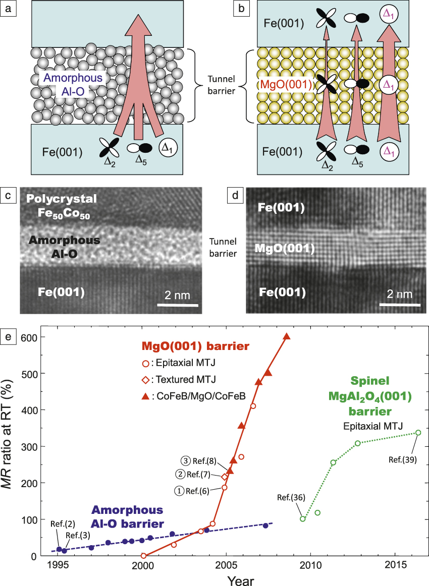
The MR ratios of Al-O-based MTJs are smaller than 100% at RT because the tunnel barrier is amorphous (Figure 2a, c). Since such an amorphous barrier has no crystallographic symmetry, various Bloch states (i.e., wave functions of conduction electrons) with different spin polarizations of the DOS can all tunnel through the barrier (Figure 2a), resulting in the tunneling spin polarization, P, below about 0.5 at RT for usual transition-metal ferromagnets. On the other hand, when the tunnel barrier is crystalline, such as MgO(001), electrons are expected to coherently tunnel through the barrier by retaining their orbital symmetries (Figure 2b, d). According to first-principles calculations, only the Δ1 states (Bloch states with spherical symmetry) dominantly tunnel through the MgO(001) barrier.Reference Butler, Zhang, Schulthess and MacLaren4,Reference Mathon and Umersky5 Because the Δ1 states of body-centered-cubic (bcc) Fe(001) are fully spin-polarized (i.e., only the majority-spin Δ1 band has DOS at E F, which means the spin polarization P = 1 by definitionReference Julliere1), high MR ratios (>>1000%) are theoretically expected.Reference Butler, Zhang, Schulthess and MacLaren4,Reference Mathon and Umersky5
Schematic of electron tunneling through (a) an amorphous Al-O barrier and (b) a crystalline MgO(001) barrier. Δ1, Δ5, and Δ2 denote wave functions of conduction electrons with specific orbital symmetries. Thick vertical arrows illustrate transport of tunneling electrons. Cross-sectional transmission electron microscope images of (c) Fe/Al-O/Fe-Co magnetic tunnel junction (MTJ) and (d) epitaxial Fe(001)/MgO(001)/Fe(001) MTJ. (e) History of the magnetoresistance ratio (MR) ratio at room temperature (RT) in MTJs. Crystalline tunnel barrier materials are essential for attaining MR ratios substantially higher than 100%.

In 2004, Yuasa et al. fabricated high-quality fully epitaxial Fe(001)/MgO(001)/Fe(001) MTJs (Figure 2d) by using molecular beam epitaxy growth and achieved MR ratios of up to 180% at RT (data point 1 in Figure 2e).Reference Yuasa, Nagahama, Fukushima, Suzuki and Ando6 Parkin et al. fabricated MTJs with a highly oriented polycrystalline (or textured) MgO(001) barrier using sputter deposition and obtained even higher MR ratios of up to 220% at RT (data point 2 in Figure 2e).Reference Parkin, Kaiser, Panchula, Rice, Hughes, Samant and Yang7 From a microscopic point of view, the fully epitaxial MTJs and the textured MTJs are basically the same.
CoFeB/MgO/CoFeB MTJs for device applications
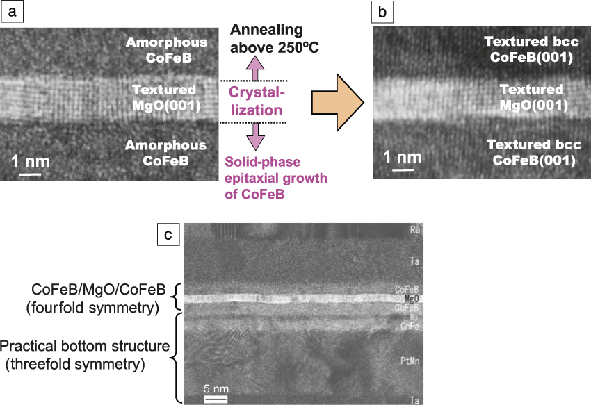
Despite their giant MR ratios, MgO-based MTJs still had the following problem for practical applications. In the practical MTJ structure shown in Figure 1b, the MTJ film should be grown on the AF/SAF multilayer, which has a fcc(111) structure, with threefold in-plane crystallographic symmetry. The problem here is that the MgO(001)-based MTJ, which has fourfold in-plane symmetry, cannot be grown on fcc(111) due to the symmetry mismatch.
Djayaprawira et al. developed CoFeB/MgO/CoFeB MTJs to solve this fundamental problem concerning the crystal growth and observed an MR ratio >200% at RT (data point 3 in Figure 2e).Reference Djayaprawira, Tsunekawa, Nagai, Maehara, Yamagata, Watanabe, Yuasa, Suzuki and Ando8 As shown in Figure 3a, amorphous CoFeB layers were formed in the as-grown state when the B concentration was higher than several atomic percent. Interestingly, a highly textured MgO(001) layer can be grown on amorphous CoFeB by sputtering under optimized conditions. When the MTJ film is annealed above ∼250°C, the CoFeB layers crystallize from the MgO(001) interfaces due to good lattice matching between MgO(001) and bcc CoFeB(001).Reference Yuasa and Djayaprawira9 This type of crystallization process is known as solid phase epitaxy. The structure after annealing is textured CoFeB(001)/MgO(001)/CoFeB(001) (Figure 3b). By using this special growth process, we can fabricate CoFeB/MgO/CoFeB MTJ films with fourfold symmetry on practical bottom structures (e.g., SAF reference layer in Figure 1b) that have threefold symmetry (Figure 3c) or basically on any kind of underlayer. The MTJs exhibit giant MR ratios of up to several hundred percent at RT (Figure 2e) because bcc CoFeB(001) has a fully spin-polarized Δ1 band at E F, the same as bcc Fe(001). Today, CoFeB/MgO/CoFeB MTJs are the mainstream technology in practical devices such as magnetic sensors and STT-MRAM.Reference Yuasa and Djayaprawira9
Cross-sectional transmission electron microscope (TEM) images of CoFeB/MgO/CoFeB magnetic tunnel junction (MTJ) (a) in as-grown state and (b) after annealing. (c) Cross-sectional TEM image of CoFeB/MgO/CoFeB MTJ with a practical synthetic antiferromagnetic reference layer structure underneath the MTJ part. Stacking structure of MTJ film is (substrate)/Ta/PtMn/CoFe/Ru/CoFeB/MgO/CoFeB/Ta/Ru/. Photo courtesy of Canon-Anelva Corporation.

STT-MRAM
Introduction
STT-MRAM is an emerging nonvolatile memory where information is written using electron spins. A typical STT-MRAM memory cell uses a one transistor, one MTJ structure, as illustrated in Figure 4a, where both the write and read operations are achieved by passing an electrical current through the MTJ. STT-MRAM technology originates from the theoretical prediction that spin-polarized electrical currents can generate a torque to switch the magnetic moment of a magnet through the transfer of angular momentum.Reference Slonczewski10–Reference Berger12 The first experimental demonstrations of the STT effect were shown in nanoparticles and spin-valve structures, and later in MTJs.Reference Sun13–Reference Huai, Albert, Nguyen, Pakala and Valet15 In 2005, Sony made the first integrated STT-MRAM chip with 4-kbit MTJ arrays using in-plane magnetized materials.Reference Hosomi, Yamagishi, Yamamoto, Bessho, Higo, Yamane, Yamada, Shoji, Hachino, Fukumoto, Nagao and Kano16 Since then, significant progress has been made, largely through materials innovations and improved device fabrication techniques. This section will focus on the materials breakthroughs that advanced the technology.
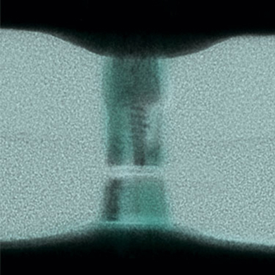
(a) Schematic of a spin-transfer-torque magnetoresistive random-access memory bit cell. (b) Cross-sectional transmission electron microscope image of a 20-nm dia. perpendicular magnetic tunnel junction (p-MTJ). Photo courtesy of IBM.

STT-MRAM with perpendicular magnetic anisotropy materials
It was recognized early on that materials with perpendicular magnetic anisotropy (PMA) would require lower STT switching currents compared to those with in-plane magnetic anisotropy, for the same activation energy (which determines data retention).Reference Sun17 However, the discovery of practical PMA materials took years. In 2008, Toshiba, together with collaborators from the National Institute of Advanced Industrial Science and Technology and Tohoku University, Japan, published the first results on integrated STT-MRAM with PMA materials, with good device data retention, fast switching, and low-switching current reported for single devices.Reference Kishi, Yoda, Kai, Nagase, Kitagawa, Yoshikawa, Nishiyama, Daibou, Nagamine, Amano, Takahashi, Nakayama, Shimomura, Aikawa, Ikegawa, Yuasa, Yakushiji, Kubota, Fukushima, Oogane, Miyazaki and Ando18 In 2010, IBM researchers reported a comprehensive evaluation of STT-MRAM devices with PMA materials integrated in 4-kbit arrays, demonstrating narrow switching voltage distributions and low write-error rate of perpendicular MTJs (p-MTJs), sufficient to fulfill the write requirements of a 64-Mb chip for the first time.Reference Worledge, Hu, Trouilloud, Abraham, Brown, Gaidis, Nowak, O’Sullivan, Robertazzi, Sun and Gallagher19 This result, based on the discovery of CoFeB-based PMA materials, led to the transition from in-plane MTJs to p-MTJs in STT-MRAM technology.Reference Ikeda, Miura, Yamamoto, Mizunuma, Gan, Endo, Kanai, Hayakawa, Matsukura and Ohno20,Reference Worledge, Hu, Abraham, Sun, Trouilloud, Nowak, Brown, Gaidis, O’Sullivan and Robertazzi21 Today, the commercialization of STT-MRAM utilizing p-MTJs is on the horizon.
PMA materials for STT-MRAM applications
In the early p-MTJ work published by Toshiba, the free-layer material was an ordered L10 alloy, which has stringent requirements for material growth, including high-temperature deposition.Reference Kishi, Yoda, Kai, Nagase, Kitagawa, Yoshikawa, Nishiyama, Daibou, Nagamine, Amano, Takahashi, Nakayama, Shimomura, Aikawa, Ikegawa, Yuasa, Yakushiji, Kubota, Fukushima, Oogane, Miyazaki and Ando18 The breakthrough on PMA materials for STT-MRAM devices came in 2009. Researchers at Tohoku University and IBM independently discovered that strong PMA (sufficient to provide good data retention) can be achieved in a thin CoFeB layer when combined with the MgO tunnel barrier.Reference Ikeda, Miura, Yamamoto, Mizunuma, Gan, Endo, Kanai, Hayakawa, Matsukura and Ohno20,Reference Worledge, Hu, Abraham, Sun, Trouilloud, Nowak, Brown, Gaidis, O’Sullivan and Robertazzi21 This work established a new class of PMA materials useful for MTJs, CoFeB|MgO, where the PMA originates from symmetry breaking at the interface, referred to as interfacial PMA (or iPMA). For the CoFeB|MgO system, the iPMA is a result of Fe(Co) 3d–O 2p orbital hybridization at the CoFeB/MgO interface.Reference Yang, Chshiev, Dieny, Lee, Manchon and Shin22 This metal/oxide perpendicular magnetic anisotropy had been discovered earlier in structures using Pt seed layers, however, the presence of Pt prevented these layers from being useful in magnetic tunnel junctions.Reference Monso, Rodmacq, Auffret, Casali, Fettar, Gilles, Dieny and Boyer23–Reference Nistor, Rodmacq, Auffret and Dieny25 Later, CoFeB-based free layers with double oxide interfaces were adopted to further enhance the free-layer PMA, which in turn, improves the thermal stability of patterned devices.Reference Kubota, Ishibashi, Saruya, Nozaki, Fukushima, Yakushiji, Ando, Suzuki and Yuasa26,Reference Sato, Yamanouchil, Ikeda, Fukami, Matsukura and Ohno27 The oxide cap also minimizes the free-layer magnetic damping (a phenomenological constant that describes the rate at which excited spins “leak” out of the free layer; this damping therefore opposes the spin torque) by cutting off the spin pumping effect (whereby spins “leak” out of the system due to spin-flip scattering caused by a nearby layer with high spin–orbit coupling) from the heavy metal cap, such as Ta, thus reducing the device switching current.Reference Konoto, Imamura, Taniguchi, Yakushiji, Kubota, Fukushima, Ando and Yuasa28
CoFeB-based PMA materials with low Gilbert damping and high tunneling spin polarization are ideal free-layer candidates for STT-MRAM devices. Requirements for reference layer materials are different. In order to minimize stray dipole field acting on the free layer in patterned devices, a synthetic antiferromagnetic (SAF) structure (see Figure 1b) is widely adopted. By adjusting the magnetic moments of the two ferromagnetic layers of the SAF, a near-zero dipole field acting on the free layer can be obtained in patterned devices. The ferromagnetic materials in the reference layers are usually PMA multilayers, including Co|Ni, Co|Pd, and Co|Pt. Besides low spin-polarization, these multilayers also have an fcc structure and tend to grow with a strong (111) texture, making them incompatible with the MgO tunnel barriers required for high TMR. By incorporating a CoFeB interfacial layer and a thin spacer layer (e.g., Ta) into the multilayer-based reference layer structure, high TMR can be achieved. Here, the spacer layer serves as a structural transition layer to ensure that the as-grown amorphous CoFeB layer crystallizes from the MgO tunnel-barrier interface and transforms into the bcc structure during the annealing process, in order to achieve high TMR.Reference Worledge, Hu, Abraham, Sun, Trouilloud, Nowak, Brown, Gaidis, O’Sullivan and Robertazzi21,Reference Hu, Topuria, Rice, Jordan-Sweet and Worledge29
The CoFeB-based iPMA-free layer, the MgO tunnel barrier, and the SAF reference layer structure are the building blocks of mainstream STT-MRAM devices, which are being actively pursued for commercialization. This material system has also shown excellent scaling potential down to sub-20 nm.Reference Kim, Kim, Jeong, Kim, Lim, Kim, Park, Shin, Park, Kim, Park, Lee, Kim, Kwon, Park, Ahn, Oh, Lee, Park, Choi, Kang and Chung30,Reference Nowak, Robertazzi, Sun, Hu, Park, Lee, Annunziata, Lauer, Kothandaraman, O’Sullivan, Trouilloud, Kim and Worledge31
New materials for next-generation MRAM
For STT-MRAM to replace high-density dynamic random-access memory, the lateral size of MTJ bits should be smaller than ∼15 nm. To maintain sufficient thermal stability of free-layer magnetization in such small bits, the PMA energy of the free layer should be larger than ∼2 MJ/m2. Moreover, an MR ratio >>300% is desired. Free-layer materials with low Gilbert damping constant α ∼ 0.001 and low saturation magnetization are also desirable to reduce the critical current density of STT switching. The CoFeB|MgO system with iPMA cannot simultaneously satisfy the requirements for ultrahigh-density STT-MRAM with 10–15-nm MTJ diameter. Therefore, p-MTJs with novel ferromagnetic and tunnel barrier materials need to be developed.
To further enhance the MR ratios, extensive experimental attempts have been made on special ferromagnetic materials called Heusler alloys such as Co2YZ-based L21-ordered alloys and Mn-based D022-ordered alloys, which have fully spin-polarized DOS at E F (i.e., only one of the majority-spin/minority-spin bands has states at E F). Moreover, half-metallic Heusler alloys theoretically have small Gilbert damping. Sakuraba et al. achieved an MR ratio of 570% at 2 K using Co2MnSi-based Heusler alloy electrodes combined with an amorphous Al-O tunnel barrier.Reference Sakuraba, Hattori, Oogane, Ando, Kato, Sakuma and Miyazaki32 This giant MR ratio showed that Co2MnSi is a half-metal, at least at low temperatures. However, the large MR ratio is substantially reduced to only 67% at RT. After the invention of the MgO tunnel barrier,Reference Yuasa, Nagahama, Fukushima, Suzuki and Ando6,Reference Parkin, Kaiser, Panchula, Rice, Hughes, Samant and Yang7 Heusler alloy electrodes have often been combined with MgO barriers, and giant MR ratios (up to 2610% at 4.2 K and 429% at RT) were reported using off-stoichiometric Co2(Mn, Fe)Si.Reference Moges, Honda, Liu, Uemura, Yamamoto, Miura and Shirai33 Note that at low temperatures, Heusler alloy electrodes exhibited higher MR ratios than CoFeB electrodes. At RT, however, the MR ratios for Heusler alloy electrodes are still smaller than those for CoFeB electrodes (up to 600%). The origin of the large temperature dependence of the MR ratio for Heusler alloys is considered to be enhanced thermal spin fluctuations at the electrode/tunnel-barrier interface. Therefore, interface engineering to suppress thermal spin fluctuations is key for practical applications of Heusler alloy electrodes.
As the MTJ bit size approaches 10 nm, the magnetic and magnetotransport properties of individual MTJ bits are likely to be strongly influenced by the presence of grains and grain boundaries in the polycrystalline MTJs, which will cause large bit-to-bit variations in properties. One way to bypass this problem is to use fully epitaxial MTJs with single-crystal barriers and electrode layers grown on Si(001) substrates. Such fully epitaxial MTJs can be integrated on large-scale integrated circuit chips using three-dimensional integration technology.Reference Yakushiji, Takagi, Watanabe, Fukushima, Kikuchi, Kurashima, Sugihara, Kubota and Yuasa34
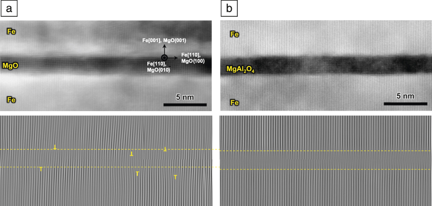
Even if we use fully epitaxial MTJs, however, many misfit dislocations form at the MgO/Fe(001) interface due to the large lattice mismatch (Figure 5a).Reference Yuasa, Nagahama, Fukushima, Suzuki and Ando6 The high density of dislocations not only causes large bit-to-bit variations, but also degrades iPMA. To substantially reduce the misfit dislocations, new crystalline tunnel barrier materials with smaller in-plane lattice constants have been developed. For example, MgAl2O4(001) spinel tunnel barriers have a much smaller lattice misfit with various ferromagnetic materials such as bcc Fe-Co and Co2YZ and Mn3Ga Heusler alloys, and are therefore suited for making MTJs with dislocation-free interfaces.Reference Shan, Sukegawa, Wang, Kodzuka, Furubayashi, Ohkubo, Mitani, Inomata and Hono36,Reference Sukegawa, Xiu, Ohkubo, Furubayashi, Niizeki, Wang, Kasai, Mitani, Inomata and Hono37 Figure 5b shows a cross-sectional scanning transmission electron microscope image of an Fe/MgAl2O4/Fe(001) fully epitaxial MTJ stack prepared by sputtering deposition. Perfectly lattice-matched interfaces without any misfit dislocations are formed in the MgAl2O4-based MTJ stack since the bulk lattice mismatch between MgAl2O4 and Fe is less than 1%, in contrast to about 3.8% for MgO/Fe. The good lattice matching in the MgAl2O4-based MTJ yields a small bias-voltage dependence of the MR ratio.Reference Sukegawa, Inomata and Mitani38 The highest MR ratio obtained for the MgAl2O4-based MTJs so far is 342%, where Co2FeAl Heusler alloy electrodes are used.Reference Scheike, Sukegawa, Inomata, Ohkubo, Hono and Mitani39 The MgAl2O4 barrier also enhances iPMAReference Sukegawa, Hadorn, Wen, Ohkubo, Mitani and Hono40 and is therefore a promising candidate as a tunnel barrier material for future ultrahigh-density STT-MRAM.
(Upper panels) Cross-sectional scanning transmission electron microscope images and (lower panels) their outlined images using fast Fourier transform filtering of epitaxial Fe/tunnel barrier/Fe(001) magnetic tunnel junctions: (a) MgO(001) barrier, and (b) MgAl2O4(001) barrier.Reference Sukegawa and Hono35 ⊥ marks indicate edge dislocations.

Conclusion
MTJs have enabled read-head technology in HDDs and are now enabling the new STT-MRAM technology. Using crystalline MgO tunnel barriers, high magnetoresistance over 200% can be achieved in practical devices. Using thin layers of CoFeB, a perpendicular magnetic easy axis can be achieved in the magnetic free layer through interfacial anisotropy with the MgO interface. These perpendicular CoFeB|MgO-based MTJs have low STT switching currents, which enable dense MRAM. Future improvements, including MgAl2O4 tunnel barriers and Heusler alloy-free layers, may enable even further scaling of this emerging technology.

Shinji Yuasa is the director of the Spintronics Research Center at the National Institute of Advanced Industrial Science and Technology, Japan. He received his BS degree in 1991, and his PhD degree in 1996, both in physics, from Keio University, Japan. His research focuses on developments related to tunnel magnetoresistance (TMR), spin-transfer torque, and spin dynamics in magnetic tunnel junctions (MTJs). He has been awarded or co-awarded more than 20 prizes for his achievement of the giant TMR effect in MgO-based MTJs, including the Asahi Award in 2007. Yuasa can be reached by email at yuasa-s@aist.go.jp.

Kazuhiro Hono is a fellow and the director of the Research Center for Magnetic and Spintronic Materials at the National Institute for Materials Science (NIMS), Japan, and is a professor in materials science and engineering at the University of Tsukuba, Japan. He received his BS and MS degrees in materials science from Tohoku University, Japan, and his PhD degree in metals science and engineering from The Pennsylvania State University in 1988. After completing postdoctoral research at Carnegie Mellon University, and as a research associate at the Institute for Materials Research, Tohoku University, he moved to NIMS as a staff scientist in 1995. His research interests include microstructure–property relationships of metallic materials, in particular, magnetic and spintronic materials and devices. Hono can be reached by email at kazuhiro.hono@nims.go.jp.

Guohan Hu is a research staff member and manager of the Magnetoresistive Random-Access-Memory Materials and Devices Group at the IBM T.J. Watson Research Center. She received her PhD degree from Cornell University in 2002. Her research focuses on magnetic oxide thin films, patterned media, and magnetoresistive random-access-memory materials. Hu can be reached by email at hug@us.ibm.com.

Daniel C. Worledge is a distinguished research staff member and the senior manager of the Magnetoresistive Random-Access-Memory Group at IBM T.J. Watson Research Center. He received his BA degree in physics and applied mathematics from the University of California, Berkeley, in 1995, and his PhD degree in applied physics from Stanford University in 2000. Since joining IBM Research in 2000, his research has focused on magnetoresistive random-access memory, including fast turnaround measurement methods for magnetic tunnel junctions and developing new perpendicular magnetic materials. Worledge can be reached by email at worledge@us.ibm.com.