I. INTRODUCTION
Direct conversion of thermal and electric energies through thermoelectric effect has attracted extensive interest in areas of waste heat recovery and environmentally friendly energy harvesting. The efficiency of a thermoelectric material is given by the dimensionless figure of merit ZT, which is defined as ZT = S 2T/(ρκ), where S is the Seebeck coefficient, ρ is the electrical resistivity, and κ is the thermal conductivity. These transport parameters are interdependent and related to the microstructure, acoustic phonon scattering at the grain boundary, atomic defects, as well as the mobility and concentration of carriers. For these reasons, maximization of ZT requires an optimization of these interdependent parameters of S, ρ, and κ.Reference Dresselhaus, Chen, Tang, Yang, Lee, Wang, Ren, Fleurial and Gogna1,Reference Lan, Minnich, Chen and Ren2 Nanostructured Bi2Te3-based materials have shown improvements to the figure of merit ZT and this was attributed to the thermal conductivity reduction by scattering of phonons at increased amounts of interfaces between nanoscale grains.Reference Poudel, Hao, Ma, Lan, Minnich, Yu, Yan, Wang, Muto, Chen, Liu, Dresselhaus, Chen and Ren3–Reference Kim, Kim, Heo and Kim7
In our previous study on nanostructured pure Bi2Te3 prepared via ball milling and the field-assisted sintering technique (FAST), the sintered samples, however, contained nanoscale porosity and exhibited high electrical resistivity and low carrier concentration that offset the reduction in thermal conductivity and increase in the Seebeck coefficient and hence compromised ZT.Reference Zhang, Sharma, Lavernia and Yang6 These observations raise the question on how to limit the increase in electrical resistivity to ultimately enhance ZT.
FAST, also known as spark plasma sintering (SPS), is a pressure-assisted sintering method that utilizes pulsed direct current heating allowing the sintering process to complete in a few minutes.Reference Munir, Anselmi-Tamburini and Ohyanagi8–Reference Omori10 It has the advantage to fabricate nanostructured Bi2Te3 alloys by providing rapid densification with minimal grain growth during powder sintering.Reference Bomshtein, Spiridonov, Dashevsky and Gelbstien4–Reference Kim, Kim, Heo and Kim7,Reference Böttner, Ebling, Jacquot, König, Kirste and Schmidt11,Reference Fan, Yang, Chen, Yun, Zhu, Bao and Duan12 In addition to the improvement on ZT through preservation of nanostructures, nanostructured Bi2Te3-based alloys present no significant texture effects on ZT and offers an mechanical property advantage to prevent cleavage along the basal plane between adjacent Te(1)–Bi–Te(2)–Bi–Te(1) layers in the  $R\overline 3 m$ space group. On the other hand, as a powder metallurgy technique, FAST poses a challenge to achieve full density, especially within a short time. Porosity can have a significant effect on ZT, even if consolidation density is over 98%, a density that is often reported in the literature.Reference Bomshtein, Spiridonov, Dashevsky and Gelbstien4–Reference Kim, Kim, Heo and Kim7 Also, it has been reported that effect of porosity may behave differently between n-type and p-type alloys.Reference Bomshtein, Spiridonov, Dashevsky and Gelbstien4,Reference Zhao, Zhang, Li, Zhang and Liu5,Reference Böttner, Ebling, Jacquot, König, Kirste and Schmidt11 Despite these efforts, a survey of the literatureReference Poudel, Hao, Ma, Lan, Minnich, Yu, Yan, Wang, Muto, Chen, Liu, Dresselhaus, Chen and Ren3–Reference Kim, Kim, Heo and Kim7, Reference Böttner, Ebling, Jacquot, König, Kirste and Schmidt11–Reference He, Hu, Tang, Lan, Yang, Wang, Hao and Chen13 suggests that an in-depth understanding of how nanoporosity influences ZT is still lacking. In light of the above, we investigated the influence of porosity on the transport properties of n-type Bi2Te3 and p-type (Bi0.2Sb0.8)2Te3 alloys and this study is undertaken as an effort to develop an FAST processing strategy to mitigate the porosity for improving ZT.
II. EXPERIMENTAL
A. Materials
Pure Bi2Te3 and Sb2Te3with a nominal particle size of 10 µm were supplied by Materion Inc. (formerly Cerac Inc., Milwaukee, WI). The Bi2Te3 powder exhibiting n-type transporting properties was sintered into bulk samples by FAST for thermoelectric properties measurement. The sintered samples of the pure Bi2Te3 composition are designated with the prefix “BT.” To obtain a p-type (Bi0.2Sb0.8)2Te3 alloy, the Bi2Te3 powder was blended with 80 mol% Sb2Te3 powder and subjected to mechanically alloying to attain a solid solution alloy prior to FAST sintering. The samples of the (Bi0.2Sb0.8)2Te3 composition are designated with the prefix “NBAT.” The mechanical alloying was conducted for 3 h using a Pulverisette 7 (Fritsch, Idar-Oberstein, Germany) planetary ball mill in a nitrogen glove box, using stainless steel vessels and tempered steel balls as the milling medium.
B. FAST consolidation
FAST consolidation experiments were carried out in an SPS-825S apparatus (SPS Syntex Inc., Kanagawa, Japan). The powders were consolidated at 673 K with axial pressures of 50, 80, or 300 MPa to obtain samples with different porosities. For the low pressure sintering experiments (50 and 80 MPa), the Bi2Te3 or (Bi0.2 Sb0.8)2Te3 powders were loaded into a cylindrical graphite die with an inner diameter of 14 mm and enclosed with graphite plungers of the same diameter. For the sintering experiments, using high pressures (300 MPa), the Bi2Te3 or (Bi0.2Sb0.8)2Te3 powders were consolidated using a tungsten carbide die set of the same dimensions as the graphite die set. The powder compacts with an initial pressure of approximately 15 MPa were heated to 373 K in 4 min. After reaching 373 K, the powder compacts were then heated to 673 K at a rate of 50 K/min and held for 3 min after reaching the target sintering temperature. For the low pressure sintering experiments, the powder compacts were subjected to a sintering pressure of either 50 or 80 MPa within 15 s after the temperature reached 363 K (samples NBAT21, NBAT41, and BT10). For the high pressure sintering experiments, the powder compacts were initially loaded to a pressure of 200 MPa within 50 s after the temperature reached 363 K. The sintering pressure was then raised to 300 MPa within 20 s after the temperature reached 498 K (sample NBAT47) and 548 K (sample BT40) for the nanostructured and 10 µm powders, respectively. A summary of sample compositions and processing parameters is listed in Table I. A disk approximately 3 mm thick was produced with each FAST experiment. The relative densities of the sintered samples were determined by both using the Archimedes method and the image analysis that was conducted by averaging 3–5 micrographs for each sample.
Processing parameters for materials in this study.

C. Material characterization
Microstructural characterization studies was performed by using x-ray diffraction (XRD) and scanning electron microscopy (SEM) in backscattered electron imaging (BEI) mode. The initial grain size of the milled powder was evaluated using XRD line profile analysis; the final grain size and porosity of the sintered bulk samples were examined using the SEM BEI images. The XRD was conducted using a Scintag XDS 2000 instrument. The BEI was conducted using JEOL 6400F (JEOL Ltd., Tokyo, Japan) at 5 kV.
Differential scanning calorimetry (DSC) was used to determine the phase transition (reaction) of the mechanically milled powder at elevated temperatures. The DSC experiments were performed in a Perkin Elmer DSC 7 apparatus (Perkin Elmer, Waltham, MA) at 40 K/min using argon as the purging gas. Alumina sample pans were used during the experiments to prevent any sample–pan interactions.
The Seebeck coefficient, electrical resistance, thermal conductivity, and carrier concentrations were measured from 2 to 400 K using a physical property measurement system (Quantum Design Inc., San Diego, CA). The carrier concentration was calculated from n = 1/R Hq, where R H is the Hall coefficient and q is the charge of a carrier. In our previous study, it was found that the FAST sintered samples from mechanically milled fine powder did not exhibit any significant texture.Reference Zhang, Sharma, Lavernia and Yang6 For convenience, the thermoelectric properties were measured from the in-plane direction of the sintered disks, i.e., perpendicular to the pressure loading direction.
III. RESULTS AND DISCUSSION
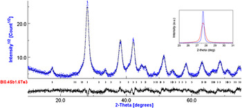
XRD patterns of the mechanically alloyed (Bi0.2Sb0.8)2Te3 powder, shown in Fig. 1, displayed the formation of a solid solution. This was further supported by the Rietveld analysis using the MAUD software (Material Analysis Using Diffraction) by Lutterotti et al.Reference Lutterotti, Bortolotti, Ischia, Lonardelli and Wenk14 No residual peaks of Bi2Te3 or Sb2Te3 were resolved. The inset in Fig. 1 shows the peak broadening effect after mechanical alloying compared with the as-received 10 μm particle powder. The grain size of the mechanically alloyed (Bi0.2Sb0.8)2Te3 powder was fitted to be approximately 16 nm.
Rietveld analysis of mechanically milled (Bi0.2Sb0.8)2Te3 powder. The inset shows XRD peak broadening after mechanical milling.

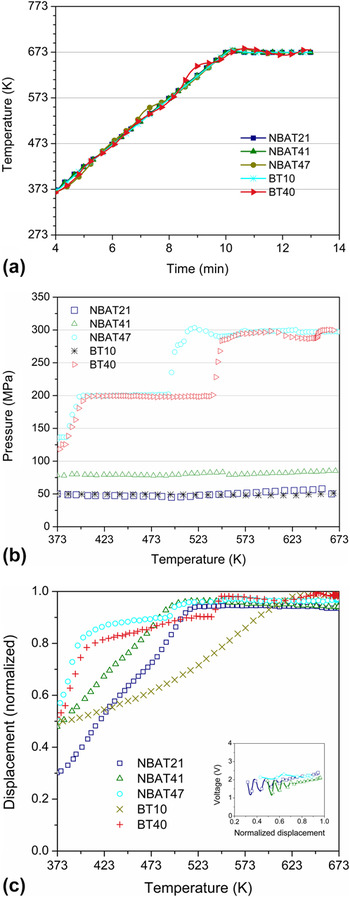
Figure 2(a) depicts the heating curve as a function of time for each sample studied. A constant heating rate was maintained for the low pressure experiments, whereas the high pressure experiments underwent slight temperature variations during increasing the load. The sintering pressure profile and displacement profile were plotted in Figs. 2(b) and 2(c), respectively, for each sample. The displacement was normalized with each sample’s final thickness for comparing the densification process among the different experiments. Note that the densification process was dependent on the sintering pressure as well as the powder size: (i) at a pressure of 50 MPa, the nanostructured powder (NBAT21) exhibited a higher densification rate than the 10 µm powder; hence the volume shrinkage in sample NBAT21 occurred mainly below ∼523 K, whereas the volume shrinkage in sample BT10 occurred in a wider range below ∼623 K; (ii) when increasing pressure to 200 MPa, the powder size effect on densification rate diminished (i.e., comparing NBAT47 with BT40) and both the nanostructured and the 10 µm powder shrank below 250 MPa. Further increasing the pressure to 300 MPa showed a slight displacement; (iii) In the low pressure experiments (50 and 80 MPa), samples NBAT21 and 41 displayed a similar densification rate, whereas the sintering pressure seemed mainly affecting the starting packing density. As a result, sample NBAT21 exhibited higher porosity (5.23%) than sample NBAT41 (2.91%) due to its lower starting packing density at 373 K; (iv) contrary to the convention that fine particle size facilitates sintering, the 10 µm powder achieved nearly full density, whereas the nanostructured powder achieved a density only at 97.55% at 300 MPa, implying that certain volatile species might be involved in the sintering process.
FAST sintering (a) temperature and (b) pressure as a function of temperature, (c) Power compact densification process versus sintering temperature.

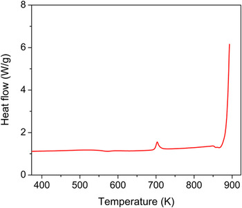
Here, the transition events during heating were characterized using DSC. As shown in Fig. 3, two endothermic peaks were detected at ∼695 and 873 K in the (Bi0.2Sb0.8)2Te3 alloy. The peak at 873 K corresponds to the melting point of the alloy, whereas the peak at 695 K is attributed to the precipitation of Te.Reference Bardi, Cafaro, Gianfreda and Piacente15 At a similar temperature (i.e., 695 K), a peak corresponding to the precipitation of Te was also recorded in the pure Bi2Te3 (not shown here). Although the sintering temperature measured from the graphite die was 673 K, the powder compact underwent a temperature gradient from the center to the surface and was subject to localized Joule heating during the FAST process.Reference Anselmi-Tamburini, Gennari, Garay and Munir16 Therefore, the powder compact may undergo local temperature variations that lead to the evaporation of Te.
DSC continuous heating curve for (Bi0.2Sb0.8)2Te3 alloy.

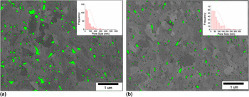
The microstructure of the sintered billets was examined using SEM under the BEI mode. Representative micrographs of samples NBAT20 and NBAT47 are shown in Figs. 4(a) and 4(b), respectively. The application of high (300 MPa) versus low (50 MPa) sintering pressure did not play a significant role in terms of the microstructural homogeneity. Heterogeneous microstructures were observed in both samples, containing regions of larger grains interlaced with smaller grains. However, the porosity in the two samples showed strong dependence on sintering pressure. In general, the pores were <1 μm and exhibited a normal distribution in both samples as shown in the set of Figs. 4(a) and 4(b), respectively. The small pore size at higher sintering pressure could be explained from the different densification curves in Fig. 2. The high sintering pressure may mitigate the contribution by the driving force of surface energy reduction. Also, the densification occurred at much lower temperatures at high pressures. Therefore, the growth of large pores at the expense of smaller pores was prohibited in the high pressure sintered samples.
BEI micrographs of FAST sintered disks (a) NBAT21 (400 °C/50 MPa) and (b) NBAT47 (400 °C/300 MPa).

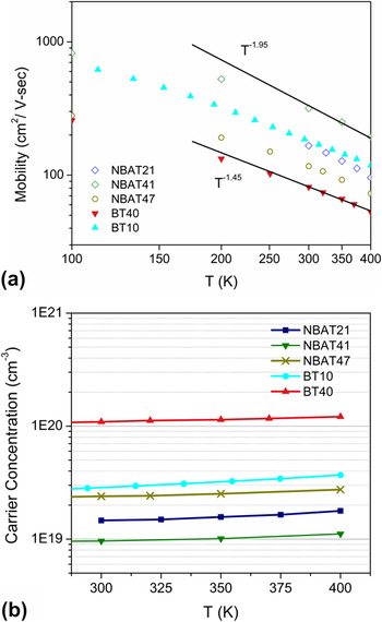
Figure 5(a) shows the temperature dependences of the Hall mobility of samples NBAT21, NBAT47, BT10, and BT40. Above 100 K, the mobility follows a power law relationship ∼T −α, where the α-value depends on the scattering mechanism. Fitted value of α for samples BT10 and BT40 was about 1.45, close to the temperature dependence of T −3/2, suggesting that the predominant scattering mechanism was acoustic phonon scattering.Reference Seeger17 The value of α for samples NBAT21 and NBAT47 was fitted to be about 1.95. This value is close to the α-value in the p-type (Bi0.2Sb0.8)2Te3 alloy reported in related studies, suggesting in addition to the acoustic phonon scattering mechanism, other mechanism such as ionized-impurity scattering should be taken into account.Reference Martin, Wang, Chen and Nolas18,Reference Caillat, Carle, Pierrat, Scherrer and Scherrer19 In Fig 5(b), the carrier concentrations are plotted against temperature. The carrier concentration increased with increasing temperature. For the (Bi0.2Sb0.8)2Te3 alloy, sample NBAT21 had carrier concentrations 1.46 × 1019 cm−3 at 300 K, sample NBAT47 had a carrier concentration of 2.39 × 1019 cm−3. In the pure Bi2Te3 material, sample BT10 showed a carrier concentration of 2.86 × 1019 cm−3, whereas sample BT40 showed a carrier concentration of 1.09 × 1020 cm−3. The nanostructured samples (NBAT21 and NBAT47) exhibited lower carrier concentrations in comparison with the coarse-grained samples (BT10 and BT40). The grain size effect on the carrier concentration is consistent with the trend observed by Kim and MitaniReference Kim and Mitani20 which suggests that the grain boundaries played the role of acceptors thereby increasing hole concentration. However, grain boundaries may also act as traps, which cannot be distinguished from acceptors from Hall effect measurements alone. Also of note is that the carrier concentration increased with high pressure sintering (300 MPa) for both the n-type Bi2Te3 and the p-type (Bi0.2Sb0.8)2Te3 alloys although each alloy used the same starting powder. This implies that the porosity evolution during FAST in each sample influences the carrier concentration. Miller and LiReference Miller and Li21 demonstrated the existence of anti-site defects  ${\rm{Bi}}_{{\rm{Te}}}^{\rm{'}}$ in Bi2Te3 through density measurements and calculating the formation energy of lattice defects. The increase in carrier concentration in BT40 compared with BT10 thus might be attributed to the decrease in hole (
 $h^ \bullet$) generation described asReference Zhang, Sharma, Lavernia and Yang6:
 $${\rm{Bi}}_{\rm{2}} {\rm{Te}}_{\rm{3}} + 2{\rm{V}}_{{\rm{Bi}}}^{'''} + 3{\rm{V}}_{{\rm{Te}}}^{{\rm{ \bullet \bullet }}} \to \!2{\rm{Bi}}_{{\rm{Te}}}^{\rm{'}} \!+ {\rm{Te}}_{{\rm{Te}}} \!+ {\rm{Te}}_{2(g)} \!+ 2h^ \bullet \quad,$$
where  ${\rm{V}}_{{\rm{Bi}}}^{'''}$ are Bi vacancies, and
 ${\rm{V}}_{{\rm{Te}}}^{{\rm{ \bullet \bullet }}}$ are Te vacancies. Higher pressure sintering led to lower porosity and densification at lower temperatures. The decreased porosity may impede the evaporation of Te as a result of the increased diffusion path, while low temperatures may slow down the reaction.
(a) Hall mobility and (b) carrier concentrations of FAST sintered Bi2Te3 and (Bi0.2Sb0.8)2Te3 samples.

Additionally, the carrier concentration is known to be sensitive to lattice defects created during mechanical milling. Navrátil et al.Reference Navrátil, Starý and Plechácek22 proposed that BixSb2−xTe3 is prone to the creation of vacancies during milling. These vacancies are generated from cleavage slip due to the weak van der Waals bonding between Te(1) and Te(1) layers. During sintering, two different reactions may occur: one producing electrons and the other producing holes. The generation of electrons can be described by the following equationReference Navrátil, Starý and Plechácek22:
 $${\rm{V}}_{{\rm{Bi(Sb)}}}^{{\rm{'''}}} \!+ 2{\rm{V}}_{{\rm{Te}}}^{{\rm{ \bullet \bullet }}} + {\rm{Bi(Sb)}}_{{\rm{Te}}}^{\rm{'}} \!\to {\rm{Bi(Sb)}}_{{\rm{Bi(Sb)}}} \!+ 3{\rm{V}}_{{\rm{Te}}}^{{\rm{ \bullet \bullet }}} + 6{\rm{e}}^{\rm{'}} ,$$
where  ${\rm{e}}\prime$ is the produced electron. Also, the volatization of Te at elevated temperatures experienced during sintering may lead to the generation of holes.Reference Starý, Horák, Stordeur and Stölzer23 The volatization of Te generates Te vacancies
 ${\rm{V}}_{{\rm{Te}}}^{{\rm{ \bullet \bullet }}}$, which are then occupied by Bi atoms. Subsequently, antisite defects and Bi or Sb vacancies are generated. The generation of holes
 $h^ \bullet$ can be described by the following equation:
 $${\rm{(Bi}}_{{\rm{0}}{\rm{.2}}} {\rm{Sb}}_{{\rm{0}}{\rm{.8}}} {\rm{)Te}}_{\rm{3}}\, {\rm{ + \,V}}_{{\rm{Te}}}^{{\rm{ \bullet \bullet }}} \to 0.4{\rm{Bi(Sb)}}_{{\rm{Te}}}^{\rm{'}} + 0.4{\rm{V}}_{{\rm{Bi(Sb)}}}^{{\rm{'''}}} \cr+ {\rm{Te}}_{{\rm{Te}}} + {\rm{Te}}_{2(g)} + 0.4h^ \bullet \quad.$$
On basis of Eqs. (2) and (3), electron and hole generation are competing processes. The p-type (Bi, Sb)2Te3 is known to be a double carrier (electrons and holes) semiconductor,Reference Xu, Niu and Wu24 i.e., acceptor defects such as  ${\rm{Bi}}_{{\rm{Te}}}^{\rm{'}}$ and
 ${\rm{Sb}}_{{\rm{Te}}}^{\rm{'}}$and donor defects such coexist in the solid solution. As mentioned before, the Te vacancy
 ${\rm{V}}_{{\rm{Te}}}^{{\rm{ \bullet \bullet }}}$ is easily produced by cleavage slip of weak van der Waals bonding between Te(1) and Te(1) layers as a result of mechanical deformation. Both Sb and Bi tend to form antisite defects (Bi/Sb on the Te sublattice). Because of the closer electron affinity between Sb and Te than between Bi and Te, a higher Sb content induces more antisite defects leading these ternary (Bi, Sb)2Te3 alloys exhibiting p-type transport behavior.Reference Zhao, Dyck, Hernandez and Burda25 During sintering, the acceptor and donor defects interact with each other and lead to change of carrier concentration as described in Eqs. (2) and (3). The results in current study suggest that either Eq. (2) (i.e., annihilation of antisite defects) or Eq. (3) (i.e., production of antisite defects) could prevail during the sintering process. For example, sample NBAT41 showed lower carrier concentration than NBAT21, whereas sample NBAT47 exhibited higher carrier concentration than NBAT21, although the sintering pressure was increased in order. Although the elimination of Te vacancies is considered to be related to Te precipitation or vaporization, the current results suggest that the carrier concentration is not strongly dependent on Te precipitation. In a related study, a similar observation was made on the effect of Te precipitation on p-type (Bi0.2Sb0.75)2Te3.Reference Hyun, Hwang, Shim and Oh26 Further investigation is needed to address of effect of sintering pressure to optimize the carrier concentration, which is critical to improve the figure-of-merit ZT. On the other hand, the effect of sintering pressure as well as mechanical milling shows a clearer trend in the n-type pure Bi2Te3. For the nanostructured Bi2Te3 powder prepared by mechanical milling, it was revealed that the excess Te vacancies produced during mechanical milling tended to anneal out during sintering and resulted in the carrier concentration dropped below 1019 cm−3 in our previous study.Reference Zhang, Sharma, Lavernia and Yang6 The result is consistent with the current study, as seen in sample BT40, the carrier concentration in the fully dense sample increased compared with sample BT10, which was attributed to the suppression of Te precipitation or vaporization during the high pressure sintering process such that the acceptor defects (holes) production was impeded as described in Eq. (1). It is noteworthy that p-type nanostructured samples was able to achieve an appropriate carrier concentration, above 1019 cm−3, for further optimizing the figure-of-merit ZT as opposite to the n-type nanostructured Bi2Te3 produced via mechanical milling.Reference Yu, Xu, Zhang, Yu, He, Liu and Tian27
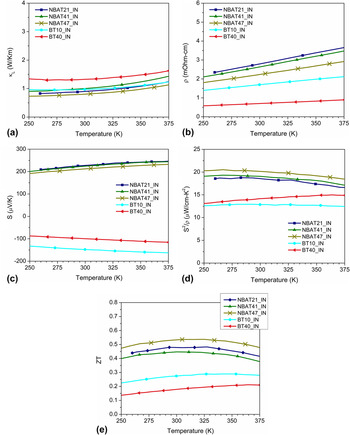
Figure 6(a) shows the temperature dependence of lattice thermal conductivity measured in the in-plane direction. The high pressure sintered sample BT40 (300 MPa) exhibited higher conductivity compared to the low pressure sintered sample BT10 (50 MPa). The increase in thermal conductivity could be attributed to the reduction of porosity. For the (Bi0.2Sb0.8)2Te3 alloy, sample NBAT41 (80 MPa) exhibited higher thermal conductivity than sample NBAT21 (50 MPa), following the trend higher pressure leading to higher conductivity. However, sample NBAT47 (300 MPa) showed even lower conductivity than NBAT21 (50 MPa). Sumirat et al.Reference Sumirat, Ando and Shimamura28 proposed an empirical model that related the thermal conductivity to pore size as follows:
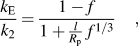 $${{k_{\rm{E}} } \over {k_2 }} = {{1 - f} \over {1 + {\textstyle{l \over {R_{\rm{p}} }}}\,\,f^{1/3} }}\quad,$$
where k E is the effective thermal conductivity and the k 2 is the thermal conductivity of the matrix. The term l is the mean free path of phonon scattering, R p is the pore size, and f is the volume fraction of pores. With decreasing the pore size, the contribution from pore scattering increases. Therefore, the reduction of pore size in sample NBAT47 is more effective in reducing the thermal conductivity.
(a) Thermal conductivities, (b) electric resistivity, (c) Seebeck coefficients, (d) power factors, and (e) ZT of the FAST sintered samples.

The electrical resistivity (in-plane direction) as a function of temperature is shown in Fig. 6(b). The nanostructured (Bi0.2Sb0.8)2Te3 samples generally have a higher electrical resistivity when compared with the coarse-grained pure Bi2Te3 samples, which was attributed to increased electron scattering by grain boundaries and porosity. Note that sample BT40 shows much lower electrical resistivity, this is also attributed to its high carrier concentration in addition to a porosity reduction. In the (Bi0.2Sb0.8)2Te3 samples, high pressure sintering (NBAT47) was more effective in reducing the electrical resistivity.
Figure 6(c) plots the Seebeck coefficient versus temperature for the (Bi0.2Sb0.8)2Te3 and Bi2Te3 samples various samples measured in the in-plane direction. The (Bi0.2Sb0.8)2Te3 samples exhibited positive values for the Seebeck coefficient (p-type), whereas the Bi2Te3 samples showed negative values for the Seebeck coefficient (n-type). Samples sintered using FAST are considered to be degenerate semiconductors, where both the Seebeck coefficient (absolute value for the n-type samples) and the electrical resistivity increased monotonically with increasing temperature. Note that at room temperature, the carrier concentration increased from 2.86 × 1019 cm−3 for sample BT10 to 1.09 × 1020 cm−3 for sample BT40. Accordingly, the Seebeck coefficient approximately decreased by 48 µV/K. The secondary factors that affect the Seebeck coefficient include thermal and electrical conductivity. In the (Bi0.2Sb0.8)2Te3 samples of which the carrier concentration is in the order of 1019 cm−3, there is an insignificant variation in the Seebeck coefficient. Bergman and LevyReference Bergman and Levy29 gave an expression describing the Seebeck coefficient as a function of thermal (k) and electrical (σ) conductivity based on the general effective medium theory (EMT):
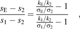 $${{s_{\rm{E}} - s_2 } \over {s_1 - s_2 }} = {{{\textstyle{{k_{\rm{E}} /k_2 } \over {{\rm{\sigma }}_{\rm{E}} /{\rm{\sigma }}_2 }}} - 1} \over {{\textstyle{{k_1 /k_2 } \over {{\rm{\sigma }}_1 /{\rm{\sigma }}_2 }}} - 1}}\quad,$$
where the effective k E or σE of a composite with two components is formulated according to the general medium theory asReference McLachlan, Blaszkiewicz and Newnham30:
 $${{{\rm{\sigma }}_{\rm{1}}^{{{\rm{1}} \mathord{\left/ {\vphantom {{\rm{1}} {\rm{\tau }}}} \right. \kern-\nulldelimiterspace} {\rm{\tau }}}} - {\rm{\sigma }}_{\rm{E}}^{{{\rm{1}} \mathord{\left/ {\vphantom {{\rm{1}} {\rm{\tau }}}} \right. \kern-\nulldelimiterspace} {\rm{\tau }}}} } \over {{\rm{\sigma }}_{\rm{1}}^{{{\rm{1}} \mathord{\left/ {\vphantom {{\rm{1}} {\rm{\tau }}}} \right. \kern-\nulldelimiterspace} {\rm{\tau }}}} + A{\rm{\sigma }}_{\rm{E}}^{{{\rm{1}} \mathord{\left/ {\vphantom {{\rm{1}} {\rm{\tau }}}} \right. \kern-\nulldelimiterspace} {\rm{\tau }}}} }} = (1 - f_1 ){{{\rm{\sigma }}_{\rm{E}}^{{{\rm{1}} \mathord{\left/ {\vphantom {{\rm{1}} {\rm{\tau }}}} \right. \kern-\nulldelimiterspace} {\rm{\tau }}}} - {\rm{\sigma }}_{\rm{E}}^{{{\rm{1}} \mathord{\left/ {\vphantom {{\rm{1}} {\rm{\tau }}}} \right. \kern-\nulldelimiterspace} {\rm{\tau }}}} } \over {{\rm{\sigma }}_{\rm{2}}^{{{\rm{1}} \mathord{\left/ {\vphantom {{\rm{1}} {\rm{\tau }}}} \right. \kern-\nulldelimiterspace} {\rm{\tau }}}} + A{\rm{\sigma }}_{\rm{E}}^{{{\rm{1}} \mathord{\left/ {\vphantom {{\rm{1}} {\rm{\tau }}}} \right. \kern-\nulldelimiterspace} {\rm{\tau }}}} }}\quad,$$
where σ1, σ2, k 1, and k 2 are the electrical and thermal conductivity, respectively, of the various components. The term f 1 is the volume fraction of component 1. τ is the scaling exponent and A = (1 − f c)/f c, where f c is the percolation threshold. The constant τ and A in Eq. (6) are usually determined by fitting experimental data. Assuming the constants τ and A in determining k E and σE are identical, from Eq. (5), the effective Seebeck coefficient S E = S 2 (assuming S 2 is the matrix). In the current composites, taking the conductivity of pores to be zero (i.e., σ1 = 0 and k 1 = 0), Eq. (6) is reduced to
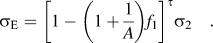 $${\rm{\sigma }}_{\rm{E}} = \left[ {1 - \left( {1 + {1 \over A}} \right)f_1 } \right]^{\rm{\tau }} {\rm{\sigma }}_2 \quad.$$
When τ = 1 and A = 2, Eq. (7) is written as the widely used EMT equation describing electrical conductivity in a porous mediumReference Lee, Vashaee, Wang, Dresselhaus, Ren and Chen31:
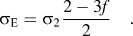 $${\rm{\sigma }}_{\rm{E}} = {\rm{\sigma }}_2 {{2 - 3f} \over 2}\quad.$$
Letting τ = 1 and A = 3.3 yields the least square fitting to the Maxwell equation which typically describes the thermal conductivityReference Sumirat, Ando and Shimamura28,Reference Lee, Vashaee, Wang, Dresselhaus, Ren and Chen31
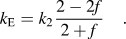 $$k_{\rm{E}} = k_2 {{2 - 2f} \over {2 + f}}\quad.$$
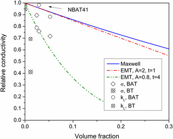
However, Eq. (5) is not applicable to the condition where σ1 = 0 and k 1 = 0. Zhao et al.Reference Zhao, Zhang, Li, Zhang and Liu5 suggested that porosity does not significantly affect the value of the Seebeck coefficient. Lee et al.Reference Lee, Vashaee, Wang, Dresselhaus, Ren and Chen31 modeled the effect of porosity on the Seebeck coefficient in SiGe and showed that bulk porosity did not change the value of Seebeck coefficient, whereas nanoporosity resulted in an increase in the Seebeck coefficient. The experimental measurement in Fig. 6(c) of the Seebeck coefficient for NBAT47 is slightly larger than NBAT21 or NBAT47, opposite to the effect of nanoporosity predicted by Lee et al.Reference Lee, Vashaee, Wang, Dresselhaus, Ren and Chen31 Hence, the slight decrease of the Seebeck coefficient for sample NBAT47 is attributed to its higher carrier concentration [Fig. 5(b)]. To evaluate the effect of porosity on the electrical and thermal conductivity on the basis of the EMT, it is necessary to obtain the σ2 and k 2 from a fully dense sample. Here, the electrical and thermal conductivity values of the matrix are calculated using the single crystal data from the Hashin–Shtrikman lower bound.Reference Hashin and Shtrikman32,Reference Helsing33 The lattice thermal conductivity for (Bi0.2Sb0.8)2Te3 was calculated to be 1.4 and 1.0 W/Km, respectively.Reference Caillat, Carle, Pierrat, Scherrer and Scherrer19,Reference Fleurial, Gailliard, Triboulet, Scherrer and Scherrer34 The relative thermal (k e/k 2) and electrical conductivity (σe/σ2) are plotted in Fig. 7. From the usual ranges for τ (1–4) and A (0.8–2) according to the published data in EMT,Reference Gelbstein35 one notices that samples NBAT21 and NBAT47 fell within the ranges, whereas samples BT40 and NBAT41 were out of these ranges as shown in Fig. 7. The power factor and ZT as a function of temperature are shown in Figs. 6(d) and 6(e), respectively. The power factor curves increase with decreasing porosity. However, NBAT41 exhibited a lower ZT value compared with NBAT21, although NBAT41 had lower porosity than NBAT21. A similar observation was made between samples BT40 and BT10. Note that the thermal or electrical conductivity values for NBAT41 and BT40 fell off the ranges predicted by EMT using the conventional A and τ values from the literature. Also, it is interesting to note that the thermal conductivity dropped with a steeper trend than the electrical conductivity for sample NBAT47, opposite to samples NBAT21 and NBAT41, where the electrical conductivity dropped with a steeper trend than the thermal conductivity. Accordingly, the high pressure sintered sample NBAT47 showed the highest ZT in the Bi2Te3-based alloys.
Plot of relative thermal and electrical conductivity vs. volume fraction of porosity.

IV. CONCLUSIONS
(1) High pressure sintering during FAST led to increasing carrier concentration. In the n-type Bi2Te3, the carrier concentration was increased from 1019 to 1020 cm−3, deviating the optimal range for optimizing ZT.
(2) High pressure sintering increased ZT for p-type (Bi0.2Sb0.8)2Te3 alloys. In the low pressure experiments (<80 MPa), the sintering pressure did not show a consistent trend on ZT.
(3) Electrical resistivity decreased with increasing sintering pressure. The pressure effect on thermal conductivity was not straightforward. The sintering pressure needs to be optimized with other factors such as porosity reduction and the carrier concentration increasing to maximize ZT.
ACKNOWLEDGMENTS
This research was supported by Sandia National Laboratories under contract no. 826008. Sandia National Laboratories is a multiprogram laboratory managed and operated by Sandia Corporation, a wholly owned subsidiary of the Lockheed-Martin Company, for the U.S. Department of Energy’s National Nuclear Security Administration under contract no. DE-AC04-94AL85000. The authors would also like to acknowledge the use of the SPS-825S system which was supported by the Office of Naval Research through the Defense University Research Instrumentation Program under grant ONR-N00014-07-1-0745. Additionally, JKY would like to acknowledge the support of the Campus Executive Fellowship from Sandia National Laboratories.