I. INTRODUCTION
Electronic devices utilizing nanowires and nanorods are subject of great interest since they promise to have novel properties and be a substitute for devices made of conventional semiconducting thin film or bulk materials. ZnO, with its wide direct band gap (3.37 eV) and large exciton binding energy (60 meV), is a promising material for various applications. Nanostructures offer grain-boundary and mostly defect-free single crystalline nature over their bulk counterparts, which could be beneficial for electronic and optoelectronic applications. Therefore, ZnO nanorods and nanowires have been a subject of intense study in recent years for their implementation in ultraviolet (UV) lasers,Reference Huang, Mao, Feick, Yan, Wu, Kind, Weber, Russo and Yang1 field emission devices,Reference Li, Zhang, Mann, Hiralal, Unalan, Lei, Wang, Chu, Piribat, Amaratunga and Milne2, Reference Zhu, Zhang, Sun, Feng, Xu, Zhao, Xiang, Wang and Yu3 sensors,Reference Santra, Guha, Ali, Hiralal, Unalan, Covington, Amaratunga, Milne, Gardner and Udrea4, Reference Wang, Summers and Wang5 transistors,Reference Li, Hsieh, Dalal, Newton, Scott, Hiralal, Nathan, Warburton, Unalan, Beecher, Flewitt, Robinson, Amaratunga and Milne6 solar cells,Reference Law, Greene, Johnson, Saykally and Yang7–Reference Unalan, Hiralal, Kuo, Parekh, Amaratunga and Chhowalla9 piezo-nanogenerators,Reference Wang and Song10, Reference Lu, Song, Lu, Chen, Gao, Chen and Wang11 light emitting diodes.Reference Jeong, Oh, Ham and Myoung12 Several methods have been utilized for the synthesis of ZnO nanowires. Vapor phase transport,Reference Wu, Wen, Tseng and Liu13, Reference Lyu, Zhang, Lee, Ruh and Lee14 metal-organic chemical vapor deposition (MOCVD),Reference Yuan and Zhang15, Reference Ye, Huang, Xu, Zhou and Wang16 and low temperature approachesReference Greene, Law, Tan, Montano, Goldberger, Somorjai and Yang17–Reference Xi, Song, Xu, Yang, Gao, Hu and Wang34 are among a few of these methods. Low temperature growth methods for ZnO nanostructures include but not limited to sol-gel method,Reference Huang and Lin35, Reference Ahn, Lee, Kim, Kim, Kang, Kim and Kim36 chemical bath depositionReference Kumar, Raj, Mangalaraj and Nataraj37 and hydrothermal methods. Hydrothermal synthesis is a robust and economic method for the growth ZnO nanowires that can be carried out with simple equipment unlike the other methods mentioned. Hydrothermal method was first introduced by Vaysseries et al.Reference Vayssieres30 for the growth of ZnO nanowires on substrates. This has been followed by seeding and annealing the substratesReference Greene, Law, Tan, Montano, Goldberger, Somorjai and Yang17 to obtain aligned nanowires. Subsequently, it has been shown that ZnO nanowires can be patterned,Reference Kim, Lee, Hong, Yi, Kim and Cheong29 can be doped with transition metalsReference Yuhas, Zitoun, Pauzauskie, He and Yang31 and their growth direction can be controlled.Reference Gao, Liu, Buchine, Weintraub, Wang and Lee32 Formation of ZnO nanotubes by a two-step hydrothermal process has also been demonstrated, in which previously grown nanowires were preferentially etched within the same solution, but at a lower temperature to form nanotubes.Reference Xi, Song, Xu, Yang, Gao, Hu and Wang34 One of the problems associated with the hydrothermal synthesis of the ZnO nanowires was the time required, which spanned from several hours to days. It has been resolved through heating the growth solution through a tip sonicatorReference Jung, Oh, Lee, Park and Jeong33 or a microwaveReference Unalan, Hiralal, Rupesinghe, Dalal, Milne and Amaratunga23 oven under ambient conditions. This allowed synthesis of high AR ZnO nanowires in matter of minutes. Researchers use capping agentsReference Xu, Adiga, Ba, Dasgupta, Wu and Wang20 or strong basesReference Zhang and Yanagisawa21, Reference Lee, Sounart, Liu, Spoerke, McKenzie, Hsu and Voigt27 to synthesize ZnO nanowires with high AR; however, these substances may introduce unwanted impurities into ZnO nanowires, which could limit their use in certain applications. In almost all of the previously mentioned studies, zinc nitrate hexahydrate has been used as the zinc source and the effects of different growth parameters on the final product have been reported using this salt.Reference Wang, Tseng, Wang, Wang, Lu and Shih19 Zinc chloride, on the other hand, is mainly preferred for electrochemical ZnO nanowire growth.Reference Elias, Tena-Zaera and Lévy-Clément38 A third alternative, zinc acetate dihydrate, which is commonly used for seeding the ZnO nanowire growth, is rarely used as a zinc source involving the hydrothermal method. Because of this, no parametric study taking into account the growth parameters using zinc acetate dihydrate salt has been ascertainable in the literature.
In this work, we report on the effect of parameters for growing ZnO nanowires via hydrothermal method using zinc acetate dihydrate as a zinc source. The effects of growth time, temperature, solution concentration and concentration ratio are investigated. Our results present a roadmap for the synthesis of ZnO nanowires with desired diameter and length using zinc acetate dihydrate as the zinc source, without any extra additives.
II. EXPERIMENTAL DETAILS
In this work, silicon (001) substrates were used to grow ZnO nanowires. All chemicals were purchased from Sigma-Aldrich and Merck Chemicals and used without further purification. Before growth process, pieces of silicon substrates were first ultrasonically cleaned, in consecutive acetone (99.8%), isopropanol (99.8%) and deionized (DI) water baths (18.3 MΩ) for 10 min. Substrates were then dried with nitrogen gas. A 5 mM solution of zinc acetate dihydrate in 1-propanol was prepared and used for the deposition of seed layer through spin coating. Right after spin coating, substrates were annealed at 350 °C for 20 min to obtain aligned ZnO nanowires. Seeded substrates were then dipped into aqueous solutions of zinc acetate dihydrate [Zn(O2CCH3)2(H2O)2, 99.0%] and hexamethylenetetramine [HMTA, (CH2)6N4, 99.0 %] at the set temperature and kept for the desired duration of time for growth. Solution concentrations (0.01–0.1 M) with zinc acetate dihydrate/HMTA concentration ratios of 3:1, 2:1, 1:1, 1:2 and 1:3 were investigated. Growth times up to 3 h at growth temperatures in the range of (50–100 °C) were elaborated. At the end of the growth process, substrates were taken out of the solution, rinsed with DI water to remove any residual salts and organic material and finally dried with nitrogen gas.
The crystal structure of the nanowires was investigated by x-ray diffraction (XRD) using a vertical goniometer axis Rigaku Cu Kα x-ray diffractometer (Rigaku Corporation, Tokyo, Japan) with the Bragg-Brentano focusing geometry. Optical absorption measurements via ultraviolet visible spectroscopy (UV-VIS) were taken using VARIAN CARY 100 BIO UV-Visible Spectrometer (Agilent Technologies Pty Ltd., Mulgrave, Victoria, Australia) in normal incidence mode from ZnO nanowires grown on quartz substrates. Conventional and high-resolution transmission electron microscopy (HRTEM) analyses were conducted using a JEOL JEM 2100F scanning/transmission electron microscope (S/TEM; JEOL Ltd., Tokyo, Japan) operated at 200 kV. Specimens for TEM analyses were prepared by drop-casting of methanolic solution of nanowires onto lacey carbon coated copper grids. Photoluminescence measurements were performed using HORIBA Jobin Yvon PL system (HORIBA Ltd., Irvine, CA) at an excitation wave length of 325 nm. The morphology and size of the ZnO nanowires were investigated by a FEI Nova Nano SEM 430 Field Emission Scanning Electron Microscope (FESEM; FEI, Eindhoven, Netherlands) at 10 kV. ZnO nanowires grown on silicon substrates were analyzed without any coating. Cross-sectional SEM analyses were conducted from the cleaved surfaces of the specimens. Length and diameter of the more than 100 individual nanowires were measured using ImageJ software from the obtained SEM images and then the average length and diameter of the nanowires were calculated and reported with their error bars.
III. RESULTS AND DISCUSSION
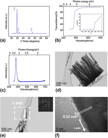
XRD spectrum from ZnO nanowires grown at 85 °C, for 3 h at an equimolar zinc acetate dihydrate and HTMA concentration of 0.02 M is shown in Fig. 1(a). The strong peak at 34.8° (2θ) corresponding to (002) spacing of the wurtzite structure [Joint Committee on Powder Diffraction Standards (JCPDS) Card No: 36–1451] revealed a preferential alignment of the nanowires on the substrate in their c-axis direction. Figure 1(b) shows the transmittance of the ZnO nanowires grown under the same conditions. Within the 3.17–6.2 eV photon energy range, almost constant and high transparency in the visible portion and a sharp absorption onset at 374 nm is observed. The band gap of the ZnO nanowires is estimated to be 3.27 eV from the Tauc plot considering the direct band gap, as shown at the inset of the graph in Fig. 1(b). Photoluminescence measurement shown in Fig. 1(c) revealed strong band edge emission at 3.3 eV without any detectable defect related emission. TEM analysis revealed further structural information. Figure 1(d) and 1(e) show bright-field (BF) images and the corresponding selected area electron diffraction (SAED) pattern [Fig. 1(e) inset] of ZnO nanowires grown using the same growth conditions at relatively low magnifications. SAED pattern from a single nanowire reveals the single crystalline nature of the ZnO with (0002) crystal planes extending along the growth direction. Further HRTEM analyses, Fig. 1(f), from the same single crystals, clearly indicates the growth of ZnO nanowire in [0001] direction. The lattice spacing along [0001] was measured as 0.52 nm and matches up with the lattice parameter of wurtzite structure across the c-axis.
(a) X-Ray diffraction pattern for ZnO nanowires grown on silicon substrates in an equimolar 0.02 M solution of zinc acetate dihydrate and HMTA for 180 min (b) UV-VIS transmission pattern of ZnO nanowires grown on quartz substrates under the same conditions. Inset shows the Tauc plot showing the change in (αhv)2 with respect to energy. (c) Photoluminescence spectra from ZnO nanowires grown on silicon substrates. (d) BF TEM image showing a group of ZnO nanowires at relatively low magnification. (e) BF TEM image and corresponding SAED pattern (inset) taken from single crystal ZnO. (f) HRTEM image of a single ZnO nanowire showing the lattice fringes along the [0001] growth direction.

A. Effect of the time on the growth process
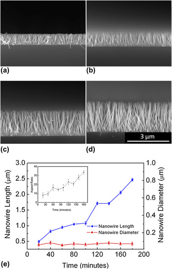
Figures 2(a)–2(d) shows the cross-sectional SEM images of ZnO nanowires that are grown at 85 °C for 40, 80, 160 and 180 min, respectively. Plot in Fig. 2(e), on the other hand shows the change in diameter and length of the nanowires with time. The graph at the inset of the plot in Fig. 2(e) reveals the change in AR of the nanowires with time. An equimolar solution of 0.02 M zinc acetate dihydrate and HMTA was used to determine the effect of growth time. As shown in Fig. 2(e), lengths of the nanowires increase steadily during the reaction period, whereas their diameters remain almost constant. At the end of 180 min, perpendicularly aligned nanowires with high AR (up to 35) were obtained. It was reported by Xu et al.Reference Xu, Adiga, Ba, Dasgupta, Wu and Wang20 that adding acetate ions to a solution of zinc nitrate hexahydrate and HMTA lead to highly responsive capping effect for growing nanowires with high AR compared with other capping agents, such as sodium dodecyl sulfate and ethylenediamine. Therefore, we attribute constancy of nanowire diameter during growth process to the capping effect of the acetate ions. Furthermore, Zhang et al.Reference Zhang and Yanagisawa21 have reported that low Zn+2/OH− concentration ratio is necessary for the growth of ZnO nanowires with high AR. We believe this condition also plays an important role in this study.
Cross-sectional SEM images of ZnO nanowires that are grown for (a) 40, (b) 80, (c) 160 and (d) 180 min. All scales are the same. (e) Variation of nanowire diameter and length with reaction time. Inset shows the variation of AR of the samples. Lines are for visual aid.

B. Effect of temperature on the growth process
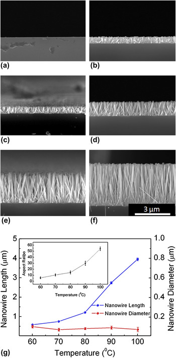
Temperature of the growth solution is another factor that has a direct influence on nanowire length and diameter. Figures 3(a)–3(f) show the cross-sectional SEM images of ZnO nanowires that are grown at 50, 60, 70, 80, 90 and 100 °C, respectively. These nanowires were grown for 3 h. Plot in Fig. 3(g) shows the change in the diameters and lengths of ZnO nanowires as a function of temperature. Lengths of the nanowires increase steadily with temperature, whereas their diameters are found to be almost constant around 80 nm. Nanowire growth was not observed for the sample kept at 50 °C. Short and stubby ZnO nanowires were observed when growth process was conducted at 60 °C. This indicates that a temperature in between 50 and 60 °C initiates the growth of ZnO nanowires in this method. It is evident that higher temperatures increase the kinetics of the reaction favoring the quick precipitation of ZnO; therefore, resulting in longer and high AR (up to 55 for the growth at 100 °C for 180 min) nanowires. This means that as the temperature of the reaction increases, the capping effect of acetate ions is getting more prominent. In addition, the resulting decrease in the concentration of Zn+2 and the Zn+2/OH− ratio in the solution due to increase in reaction kinetics may also contribute to keep the diameters of the nanowires constant.
Cross-sectional SEM images of ZnO nanowires that are grown at (a) 50 °C, (b) 60 °C, (c) 70 °C, (d) 80 °C, (e) 90 °C and (f) 100 °C. All scales are the same. Insets in (d) and (e) show the top view SEM images of the nanowires. (f) Variation in the diameter and length of ZnO nanowires with temperature. Inset shows the variation of AR of the same samples. Lines are for visual aid.

C. Effect of the concentration ratios on the growth process
Figures 4(a)–4(e) show the cross-sectional SEM images of ZnO nanowires that are grown at HMTA and zinc acetate dihydrate solution concentration ratios of 3:1, 2:1, 1:1, 1:2 and 1:3, respectively. Nanowires were grown at 85 °C for 3 h. The effect of different concentration ratios on the diameters and lengths of ZnO nanowires as a function of concentration ratios of HMTA and zinc acetate dihydrate is plotted at in Fig. 4(f). The reactions that are taking place during the ZnO nanowire growth areReference Xu, Adiga, Ba, Dasgupta, Wu and Wang20:



Cross-sectional SEM images of ZnO nanowires that are grown with solution concentration ratios of ([HMTA]/[zinc acetate dihydrate:(ZAD)]) (a) 3:1, (b) 2:1, (c) 1:1, (d) 1:2 and (e) 1:3. All scales are the same. (f) Graph showing the effect of different solution concentration ratios of HMTA and zinc acetate dihydrate on the diameter and length of ZnO nanowires. Lines are for visual aid.

From these reactions, it appears that the formation of 1 mol of ZnO product requires one-half mol of (CH2)6N4 and 1 mol of Zn(O2CCH3)2(H2O)2 which is equivalent to [(CH2)6N4]/[(Zn(O2CCH3)2(H2O)2] ratio of 1/2. So, one may expect to obtain longest ZnO nanowires using this ratio. However in our study, longest ZnO nanowires were obtained at a HMTA/zinc acetate dihydrate ratio of 1. Excess amount of (CH2)6N4 provides sufficient amount of OH− ions for the growth of ZnO nanowires in the solution, where actual concentration of NH3 is less than the nominal concentration. In this respect, our results are similar to the ones obtained during ZnO nanowire growth using zinc nitrate hexahydrate.Reference Wang, Tseng, Wang, Wang, Lu and Shih19 On the contrary to nitrate growth, we have not observed a change in the alignment and nucleation density of the nanowires with HMTA/zinc acetate dihydrate ratio at least for the nanowire morphology.Reference Wang, Tseng, Wang, Wang, Lu and Shih19 When the ratio of the concentration of zinc acetate dihydrate is higher, the structure of ZnO deviates from nanowires to a thin film-like form. This condition is related to an increase in Zn+2/OH− concentration ratio, which in turn decreases the length and AR of ZnO nanowires yet increases their diameter. On the other hand, higher HMTA ratios in comparison with zinc acetate dihydrate led to an increase in the AR of ZnO nanowires. This is due to the higher availability of OH− ions that leads to the precipitation of more ZnO compared with other concentration ratios.
D. Effect of solution concentration on the growth process
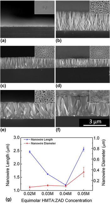
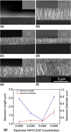
Figures 5(a)–5(f) shows the cross-sectional SEM images of ZnO nanowires grown in an equimolar ratio of zinc acetate dihydrate and HMTA solution which has zinc acetate dihydrate and HMTA concentrations of 0.01 M, 0.02 M, 0.03 M, 0.04 M, 0.05 M and 0.1 M, respectively. The effect of different concentrations on the diameters and lengths of ZnO nanowires as a function of equimolar concentrations of HMTA and zinc acetate dihydrate is plotted in Fig. 5(g). Nanowires were grown at 85 °C. Only a few nanowires are observed on the silicon substrates for the samples grown at a solution concentration of 0.01 M. It is clear that the growth of these nanowires was not originated from the seeds on the silicon substrates and they get attached to the substrate during precipitation. Thin and long nanowires were observed for a solution concentration of 0.02 M. With the increase in solution concentration to 0.05 M, an evident increase in the nanowire diameter was observed. This is a result of existence of more Zn+2 ions compared with OH− ions in the growth solution which influences the growth of the nanowires from the side planes. A film-like morphology was observed for the nanowires grown at a solution concentration of 0.1 M. Nanowire features and more prominently hexagonal facets of ZnO can still be seen within the thin film morphology, which clearly indicates that the capping effect of acetate ions have been impeded. Optimum concentration was then determined to be 0.02 M leading to the growth of high AR ZnO nanowires.
Cross-sectional SEM images of ZnO nanowires grown in solutions for 180 min containing equimolar (a) 0.01 M, (b) 0.02 M, (c) 0.03 M, (d) 0.04 M, (e) 0.05 and (f) 0.1 M zinc acetate dihydrate (ZAD) and HMTA. All scales are the same. Inset shows top view SEM images of the samples grown at indicated concentrations. (g) Graph showing the effect of different equimolar solution concentrations of HMTA and zinc acetate hexahydrate on the diameter and length of ZnO nanowires. Lines are for visual aid.

Although using highly basic growth solutions with sodium hydroxide (NaOH) and zinc nitrate hexahydrate yields high AR nanowires (AR of 15 within 60 min),Reference Lee, Sounart, Liu, Spoerke, McKenzie, Hsu and Voigt27 this may introduce impurities to nanowires. Capping agents like acetate ions or sodium oxalate can be used for the growth of high AR ZnO nanowires, but similarly, they could introduce impurities. In addition, longer reaction times were found to be necessary for the growth of the ZnO nanowires with capping agents. For instance, an AR of 20 was obtained in 36 h when acetate ions were added to the growth solution,Reference Xu, Adiga, Ba, Dasgupta, Wu and Wang20 whereas an AR of 120 in 24 h were obtained through the addition of sodium oxalate (Na2C2O4).Reference Li, Yang, Yu, Chen, Ma, Zhang, Song and Gao22 On the contrary, the use of zinc acetate dihydrate, as described in this paper, leads to the formation of ZnO nanowires in short reaction times without impurities and eliminating the need for using extra capping agents. This is evident with the obtained AR of 55 for the growth conducted at 100 °C for 180 min. Full control over the lengths and diameters of the nanowires with the synthesis parameters provided herein would facilitate the realization of ZnO nanowire-based electronic and optoelectronic devices in short reaction times without impurities.
IV. CONCLUSIONS
To conclude, ZnO nanowires have been grown using zinc acetate dihydrate as the zinc salt and the effect of growth parameters such as time, temperature, solution concentration and concentration ratios of the precursor chemicals have been determined. The use of zinc acetate dihydrate, which has acetate ions, enhances the capping effect and leads to the growth of high AR ZnO nanowires. The lengths of the nanowires were found to be controlled through the growth time and solution concentration. On the other hand, the diameters of the nanowires were found to be controlled by the precursor concentration ratio and solution concentration. Thin film morphology was obtained through the growth conducted with a high zinc acetate dihydrate concentration as compared with HMTA and at high solution concentrations. The results reported in this article establishes the basis for the growth ZnO nanowires via hydrothermal growth using zinc acetate dihydrate as the zinc source.
ACKNOWLEDGMENTS
This work was supported by the Scientific and Technological Research Council of Turkey (TUBITAK) under Grant No. 109M084 and 109M487 and the Distinguished Young Scientist Award of the Turkish Academy of Sciences (TUBA).