I. INTRODUCTION
L10-FePt small grain having high magnetic anisotropy is one of the promising candidates for the ultrahigh density magnetic or heat-assisted magnetic recording. Epitaxial c-axis oriented FePt nanoparticles were synthesized on Si(100) using TiN intermediate layer as a template.Reference Trichy, Chakraborti, Narayan and Prater1 From a detailed analysis of structure–magnetic property correlations, it was shown that individual nanoparticles in a single domain state have larger coercivity than continuous thin film. Magnetic multilayers on nanospheresReference Albrecht, Hu, Guhr, Ulbrich, Boneberg, Leiderer and Schatz2 and the template-directed self-assembled magnetic structuresReference Kappenberger, Luo, Heyderman, Solak, Padeste, Brombacher, Makarov, Ashworth, Philippe, Hug and Albrecht3 have been reported.
We have already reported that isolated FePt crystal grains having 7 nm average diameter can be fabricated directly on flat SiO2/Si substrate by rapid thermal annealing (RTA)Reference Itoh, Aoyagi, Tsukamoto, Nakagawa, Itoh and Katayama4 with out any intermediate layers. It is also reportedReference Itoh and Tsukamoto5 that nanodent array (NDA) made by using the polymer micelles technique is effective for increasing the grain density of FePt fabricated on it.
This paper describes the method of fabrication for the single layer of self-assembled silica nanoparticles (SASP) having small diameter silica spheres, as small as 18 nm. It also reports in detail that the grain density N p of FePt can be fabricated on the different substrates. The comparison of the value of N p for FePt and FeCuPt fabricated on the different substrates such as flat SiO2, NDA, and SASP has been shown. The results of the electron diffraction measurements and magnetic hysteresis loops are also shown.
II. FABRICATION OF SASP
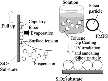
Figure 1 shows the method of making the monolayer particle array. The toluene solution includes silica particles and polymethylphenylsilane (PMPS). The role of the PMPS is to reinforce the adhesion between the silica particles and the thermally oxidized Si substrates. After dip coating, the film is exposed to ultraviolet rays (365 nm) for 90 s. Finally, a self-assembled silica particle layer was formed through an annealing process (423 K, 10 min).
Dip-coating method.

The speed of pulling the substrate up from the toluene solution is the major factor for making a fine SASP layer. The number of silica particles and the relative amount of PMPS in the solution are also important factors to achieve a mono layer of particles. The latter strongly affects the viscosity of the solution.
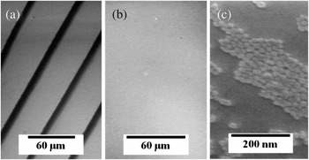
We tried to choose the optimum pulling-up speed. SEM images of the silica particles array made under a variety of pulling-up speeds are shown in Fig. 2. For the cases of 1 and 20 μm/s, the surfaces show a stepwise structure and a partial distribution of silica particles, respectively. When the pulling up speed was 10 μm/s, uniform distribution could be successfully obtained.
SEM plane view of silica particles prepared under the variety of pulling up speed. (a) 1 μm/s, (b) 10 μm/s, and (c) 20 μm/s.

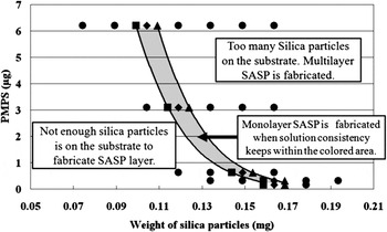
The viscosity of solution was adjusted. As mentioned previously, the total amount of silica particles in the solution is another important factor to achieve a monolayer of SASP.
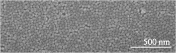
Figure 3 shows the alignment of silica particles as a function of PMPS and silica particles in 20 g of toluene solution. In the narrow shaded area shown in Fig. 3, the monolayer structure has been successfully obtained. On the other hand, other structures were obtained in two regions. A multilayer SASP was obtained in the high silica particle content region. In the low silica particle content region, there were not enough particles to fabricate the layer. The SEM plane image of obtained SASP monolayer is shown in Fig. 4.
Alignment of silica particles as a function of PMPS contents and silica particles in 20 g of toluene solution.

SEM plane view of SASP, prepared by pulling-up speed of 10 μm/s, 8.0 × 10⁻⁴ wt% of silica particles and 0.19 wt% of PMPS in toluene solution.

III. FABRICATION OF FePt GRAINS ON SASP
We deposited Pt/Fe double layer (total thickness T is 3.75 nm or 1.88 nm) by the direct current (DC) magnetron sputtering method. The base pressure of the sputtering chamber was 3.0 × 10⁻⁴ Pa. The sputtering gas is ArH (H: 3 vol. %), and the pressure was 1.8 × 10⁻¹ Pa. After deposition, Pt/Fe double layer was annealed by RTA to obtain L10-FePt crystalline by using 3 kW tungsten lamp with a heating up rate of 30 to 80 K/s. The base pressure of the annealing chamber was 5.0 × 10⁻⁴ Pa.
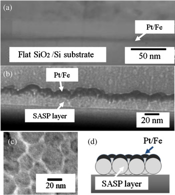
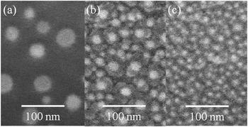
We found the differences in morphology of Pt/Fe with deposited double-layer films between SASP and flat SiO2 substrates. Figure 5 shows TEM images of Pt/Fe double layer on SASP and on the flat substrate. In these cases, T is 3.75 nm [Pt(2.02 nm)/Fe(1.73 nm)]. On the flat SiO2 substrate, the double layer is flat and continuous, as can be seen in Fig. 5(a). In contrast, with SASP, as seen in Figs. 5(b) and 5(d), the Pt/Fe double layer covers the top of every particle. The most distinguishing feature is that the double layer forms an island structure. Figures 6(a), 6(b) show the in-plane SEM images of FePt grains annealed by RTA on (a) flat SiO2/Si substrate and (b) on SASP, respectively. It is clear that SASP is effective to reduce the average grain size D a, and increase N p. D a and N p of FePt grains on SASP were 14.8 nm and 0.74 Tparticles/in.Reference Albrecht, Hu, Guhr, Ulbrich, Boneberg, Leiderer and Schatz2, respectively, while FePt grains on flat SiO2 substrate had D a = 29.6 nm and N p = 0.16 Tparticles/in.Reference Albrecht, Hu, Guhr, Ulbrich, Boneberg, Leiderer and Schatz2. When the thickness of initial bilayer was thinner—such as Pt (0.87 nm)/Fe (1.01 nm), T = 1.88 nm, on SASP—D a decreased to 5.1 nm, and N p increased up to 5.4 Tparticles/in.2, as shown in Fig. 6(c).
Cross-sectional TEM images of as-deposited Pt/Fe double layer on the (a) flat substrate and (b) SASP. (c) In-plane TEM image of (b). (d) Pt/Fe grown on SASP as island structure.

SEM plane views of FePt particles on (a) Flat SiO2 substrate (thickness of Pt/Fe: 3.75 nm), (b) SASP (thickness of Pt/Fe: 3.75 nm), (c) SASP (thickness of Pt/Fe: 1.88 nm).

IV. COMPARING GRAIN DENSITY OF FePt GRAINS ON NDA, FLAT SUBSTRATES, AND SASP
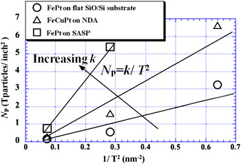
The influence of difference in nanostructure of substrates on N p was investigated in detail. The areal density b was defined as the total area of grains per unit area. FePt grains on different kinds of substrates show the same b and are not dependent on grain size and initial total thickness T. However, N p is strongly dependent on T and the substrate. Then, we assumed average grain radius D a is proportional to the T, namely D a = 2RT, where R is a constant and confirmed experimentally. Under the assumption of D a = 2RT, N p was derived as N p = k/T 2, where k is a constant. k shows the highest value with SASP, as shown in Fig. 7.
N p as a function of k/T 2. k shows the highest value for grains on silica particles.

V. XRD OBSERVATIONS OF FePt GRAINS ON SASP
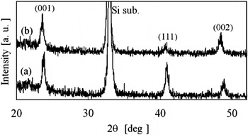
FePt (T = 3.75 nm) grains on SASP were measured by XRD and I R = I (001)/I (111), which reflects the degree of (001) crystal orientation, given in Fig. 8(a).
XRD profile for (a)FePt and (b)FeCuPt grains with the initial film thickness T = 3.75 nm.

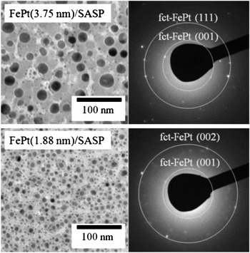
For the case of FePt grains of T = 1.88 nm, it was difficult to obtain clear peaks in the XRD profile because the grains were too small. Therefore, we tried to observe grains by electron diffraction method. Figure 9 shows plane-view bright-field TEM micrographs and selected area (300 nm diameter) electron-diffraction patterns. The patterns which corresponds to a mixture of ordered and disordered FePt crystalline have been found when T = 3.75 and T = 1.88 nm.
TEM bright-field images and diffraction spot patterns of FePt grains prepared on SASP with different initial Pt/Fe film thickness of (a) 3.75 nm and (b) 1.88 nm. Circles are guides to the eye.

VI. MAGNETIC MEASUREMENT OF Cu-DOPED FePt GRAINS ON SASP
Grain density N p shows the highest value for FePt fabricated on SASP. We reportedReference Itoh, Itoh, Nanba, Adachi, Motohashi and Tsukamoto6 that Cu doping is effective in raising I R of FePt grains on the flat SiO2/Si substrate prepared by RTA. Also on SASP, Cu doping is effective to raise I R, as shown in Figs. 8(a) and 8(b). The value of I R is 3.8 for FeCuPt, while it is 1.4 for the FePt.
High I R value results the high uniaxial magnetic anisotropy K u perpendicular to the film plane, and then it reflects to the magnetic hysteresis loops.Reference Weller, Moser, Folks, Best, Lee, Toney, Schwickert, Thiele and Doerner7, Reference Klemmer, Hoydick, Okumura, Zhang and Soffa8
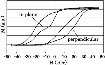
Figure 10 shows the magnetic hysteresis loops of FeCuPt [Pt(1.84 nm)/Fe(1.44 nm)/Cu(0.47 nm), T = 3.75 nm] on SASP measured by SQUID. H c is 20 kOe for the perpendicular direction, which is larger than the H c for the parallel direction (7.8 kOe). This corresponds to K u of FeCuPt grains on SASP, which has a perpendicular component to the film plane.
Magnetic hysteresis loops of FeCuPt after RTA of initial thickness 3.75 nm = Pt (1.84 nm)/Fe (1.44 nm)/Cu (0.47 nm), on SASP.

VII. SUMMARY
We investigated FePt grains fabricated on SASP and compared the grain density on NDA and flat SiO2.
(1) Monolayer SASP with small silica spheres, such as 18 nm in diameter, was successfully obtained by choosing the proper condition of solution and the speed of pulling the substrate up from it.
(2) The initial morphology of Pt/Fe double layer on the SASP is quite different from that on the flat SiO2 substrate.
(3) The experimental results show N p = k/T 2. FePt grains on SASP shows the largest k and N p and the smallest D a value among the three different substrates, such as SASP, NDA, and flat SiO2/Si.
(4) By the electron diffraction measurement, even in the smallest grain diameter of 5.1 nm obtained on SASP, we confirmed the existence of (001) oriented L10-FePt grains.
(5) Cu addition is effective to enhance the perpendicular magnetic anisotropy of FePt grain, and the square magnetic hysteresis curve was confirmed in FeCuPt on SASP.
These results show FePt and FeCuPt grains on SASP have great possibility for ultrahigh-density magnetic recording.
ACKNOWLEDGMENTS
This work is partially supported by a Grant-in-Aid for Scientific Research from MEXT in Japan, No. 21560368, and Storage Research Consortium, and Nihon University Strategic Projects for Academic Research.