I. INTRODUCTION
In multi-service and multi-band communication systems, a diplexer is an essential component, which isolates a power transmit stage from a sensitive receive stage sharing a common port (e.g. an antenna). With the booming of new commercial wireless and mobile communication systems, the demands for diplexers are increasing rapidly.
This paper presents the design and preliminary test results of a new type of a diplexer for next generation terrestrial radio-link telecommunications in E-band (71–76 and 81–86 GHz). At such frequencies, planar band-pass filters have resonators with unloaded Qs that are usually too low for most communication system requirements. Cavity- and coaxial-resonator filters offer very high Qs, but they are bulky and cannot be integrated with planar circuitry. On the other hand, micromachining technology is an attractive alternative combining high RF performance with tiny mass and volume. Qs above 1000 have been measured in micromachined Ka-band filters operating with the TE101 resonant mode [Reference Stickel, Kremer and Eleftheriades1–Reference Wang, Ke and Lancaster3]. Micromachined cavities have also been employed for low-loss band-pass filters at both lower and higher frequencies [Reference Papapolymerou, Cheng, East and Katehi4–Reference Pelliccia, Farinelli and Sorrentino8], allowing for easy surface-mountable integration. A further reduction of the filter footprint can be obtained with a multilayer approach by staking several cavities [Reference Harle and Katehi5, Reference Pelliccia, Farinelli and Sorrentino8]. Micromachining technology can be exploited for alternative resonator-cavity concepts as in [Reference Pelliccia, Farinelli and Sorrentino8]. Qs around 500, 8–10 times higher than with conventional substrates has been demonstrated in [Reference Blondy, Brown, Cros and Rebeiz9, Reference Chatras, Blondy, Cros, Vendier and Cazaux10] using bulk micromachining to remove the substrate and realize suspended-resonators. Ka-band filters have been developed in conjunction with substrate integrated waveguide (SIW) technology in [Reference Yuanwei, Yong and Jian11, Reference Khandelwal, Bansal and Rangra12]. Among all these micromachined solutions proposed in the literature, filter employing micromachined cavities with folded channel paths can be considered the best trade-off in terms of resonator unloaded Q (i.e. filter insertion loss) and footprint minimization. Surface mounting compatibility can be obtained by properly designing both the input and the output ports on the same layer. It is also worth noticing that micromachining technology presents manufacturing tolerances significantly lower than mechanical cavities fabricated using milling process. This allows for realizing tuneless cavity-resonators with high manufacturing yield leading to very robust filter response. Moreover, micromachining process, in the case of a mass production, can offer a significant cost saving with respect to milling process or other conventional fabrication approaches.
The diplexer here presented is a robust and low-cost solution using micromachined resonant cavities etched on silicon layers. The proposed manufacturing process provides a tuneless and compact device (<20 × 20 × 2 mm) without compromising the unloaded Q (roughly 1000) with respect to other solutions using mechanical waveguide technologies based on milling process. First the topology and architecture solutions are presented on the basis of the electrical requirements. Then, the design of the diplexer is introduced along with a brief description of the manufacturing process. The most of the details of the manufacturing process and test cannot be presented since they are owned by the funder institute of the project (Huawei Technologies Italia Srl, Milano) that is gratefully acknowledged for the permission of publishing the results here shown.
II. PROPOSED SOLUTION
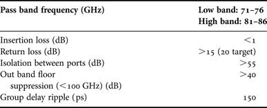
The evaluation and the study of filter specifications is the first step in a diplexer design. The electrical specifications on the desired diplexer are summarized and shown in Table 1.
Summary of the diplexer specifications.

The equiripple bandwidths of the two pass bands (low and high) are 6 GHz wide and they are centered at 73.5 and 83.5 GHz, respectively. The insertion loss (IL) in both the pass bands has to be less 1 dB and the target for the return loss (RL) is above 15 dB. In order to fulfill the diplexer isolation requirements (>55 dB) each filter consists of eight resonators implemented as TE101 mode cavities coupled together using inductive irises. The topology of the diplexer and its three-dimensional (3D) high frequency structural simulator (HFSS) model are shown in Fig. 1. The two filters are connected to the common input port by an E-plane T-junction. All ports are on the same side to simplify the interconnections with the other sections of the RF system.
Diplexer topology and diplexer 3D HFSS model.
As depicted in Fig. 1, the common T-junction is directly coupled to the waveguide common input and to the two filters. The T-junction is constituted by a step providing two E-plane bends allowing the 90° rotation of the EM field from the common port to the two filters. The advantages of using this topology are the higher isolation between channels (because they are physically separated) and the lower sensitivity to tolerances (the two filters independent one to the other). Since one of the most important goal is minimizing the overall diplexer footprint, the input and output interfaces (i.e. WR12 standard rectangular waveguides) are coupled directly to the last resonators of each filter as shown in Fig. 1, the sections of length of the junction for both the channels are minimized and the filter path is folded in an U-shape. The obtained overall footprint is less than 20 × 20 mm and the total filter height is 1.5 mm.
The design procedure begins with the design of the two filters independently; one of them meeting the desired performance in the low band (71–76 GHz) and the other desired performance in the high band (81–86 GHz).
Once the filter topology and geometry were identified, each filter has been designed separately as well known and explained in [Reference Cameron, Kudsia and Mansour13]. The pass bands of the filters have been designed a few larger so as to ensure the fulfillment of the requirements even in the case of temperature drifts. All the other design rules provided by the selected foundry have been carefully considered during the design procedure. For instance, the non-perfect verticality of the micromachined cavity side walls, due to the process, has been considered and included in the full-wave design.
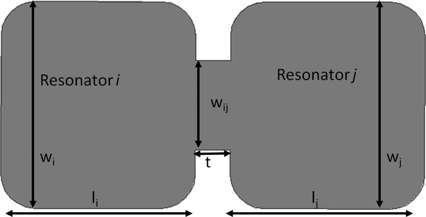
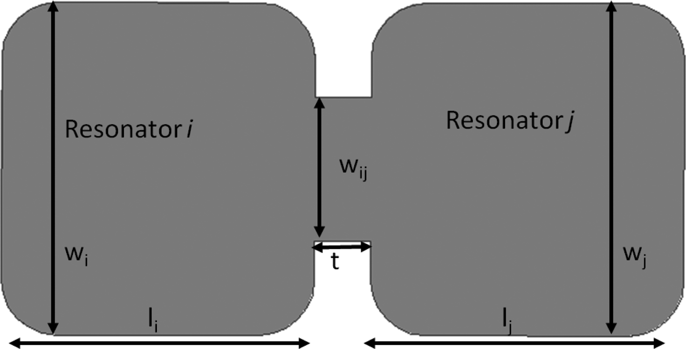
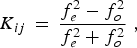
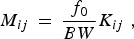
With respect to Fig. 2 the inductive inter-resonator coupling coefficient between resonators i and j (K ij) can be calculated as in (1) by varying W ij that is the width of the coupling iris between adjacent cavities, considering that the larger W ij, the larger the coupling; the coupling coefficient K ij is related to normalized coupling element M ij by (2):
Two coupled resonators.
 $${K_{ij}}\, =\, \displaystyle{{f_e^2 - f_o^2 } \over {f_e^2+f_o^2 }}{\rm \; \comma \; }$$
 $${M_{ij}}\, =\, \displaystyle{{{f_0}} \over {BW}}{K_{ij}}{\rm \; \comma \; }$$
Where the subscripts e, o refer to the even and the odd resonance, respectively. In the waveguide structures, the even and odd resonances are obtained by replacing the symmetry plane with a magnetic or electric wall, respectively. f 0 is the central frequency, BW is the equiripple bandwidth of the filter, and l i, l j that are the lengths of each adjacent resonator used in order to keep fixed the central frequency can be calculated as in (3); actually, as explained in [Reference Sorrentino and Bianchi14], those quantities are determined by the condition that the resonant frequency is equal to the center frequency f 0. Since the resonant mode is the TE101, such a condition leads to:
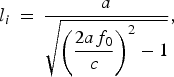 $${l_i}\, =\, \displaystyle{a \over {\sqrt {{{\left({\displaystyle{{2a{f_0}} \over c}} \right)}^2} - 1} }}\comma \;$$
where c = 1/√με is the phase velocity in the medium filling the waveguide (i.e. air).
In the design W i = W j and t are the same for each filter, so only W ij and l i, l j have been changed; the first one in order to achieve the desired level of coupling and the latest in order to keep the resonant frequency at the center frequency f 0. The distance t is the minimum feasible distance between two cavities according to the manufacturing constraints and is 0.2 mm.
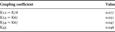
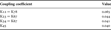
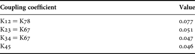
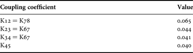
The coupling between two resonators is optimized so that the K ij is the same as that calculated starting from the low-pass prototype function, as presented in [Reference Sorrentino and Bianchi14]. K ij are shown in Tables 2 and 3, for the low band and the high band, respectively.
Summary of the diplexer specification for the low band.
Summary of the diplexer specification for the high band.
For each of these cavities, the unloaded Q at resonance is governed mainly by the height of the cavity itself. In this case a height of 0.750 mm has been chosen and the unloaded Q is ~1500. Such a value is considered enough to ensure the desired IL of both the pass bands below 1 dB. Gold-plated surfaces with a negligible roughness (<0.5 µm) are considered as internal surfaces of the etched cavities.
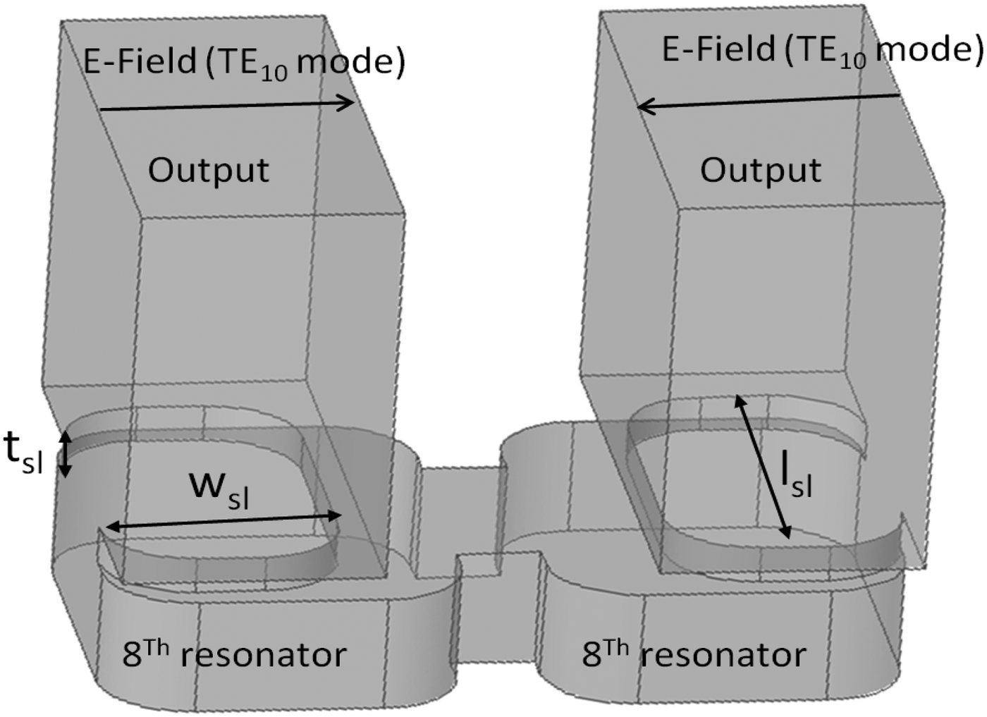
For the low band output and the high band output the couplings have been figured out, as shown in Fig. 3, by matching the S-parameters of an equivalent circuital model, based on only two ideal resonators and the desired coupling to the input/output waveguides, and the full-wave simulation in HFSS of the structure corresponding to the circuital model. The external coupling slots with rectangular WR12 waveguides have rounded corners (0.5 mm).
The structure used for the output simulation.
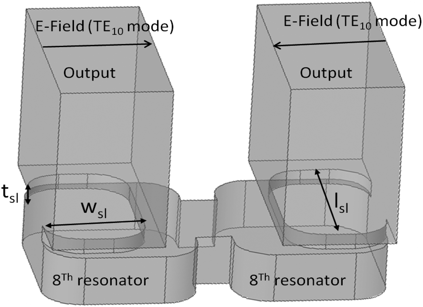
The input/output coupling element is a slot placed between the input waveguide and the 8th resonator. The width and the length of the slot, wls and lsl, respectively, are changed in order to reach the desired level of matching. As an example the case of low band filter is shown in Fig. 4.
Comparison between circuital and full-wave simulations value for the low band filters output.
The details of the E-plane T-junction are shown in Fig. 5. The step sizes are controlled and chosen in order to allow the E-plane T-junction to work in the entire E-band, i.e. from 71 to 86 GHz, as shown in Fig. 6. Once the two filters and the T-junction have been separately completed, they are united in a single full-wave design. The waveguide distances between the first-irises of each filter and the T-junction step are optimized to ensure the desired RL in the pass bands. During the final optimization of the whole diplexer also the width of the first irises and cavities of the filters have been used as degrees of freedom and varied in order to match the requirements.
Common T-junction with direct coupling to waveguide input.
Full-wave simulated performance for the common T-junction.
III. FABRICATION
The TE101 mode micromachined cavities constituting the filters of the diplexer are realized by etching two staked silicon wafers. After the etching, the wafers are gold-plated and finally staked together. The micromachined cavities are not etched perfectly vertically but with a minimum angle to guarantee a good adhesion of the seed layer for gold plating. The adopted micromachined process allows for very low manufacturing and assembly tolerances, thus the manufacturing yield of the component is expected to be very high. The manufacturing tolerances along x and y axis (cavity sizes) are different from the z dimension (cavity depth): the tolerance on the photolithography, assembly procedure as well as on the etching angle mainly affects the planar dimensions (x and y), whereas the initial wafer thickness mainly affects the cavity thickness. The resulting total tolerance for each dimensions are however below 5 µm. The measured errors are most times systematics for the full production lot, even though few parameters could vary between the center and the external sides of the circular wafer as it is in most micromachined processes.
The low manufacturing tolerances make the present technology a good candidate for high-frequency applications, even above 100 GHz. However, since at high frequency the cavity dimensions are pretty small, the devices could be very sensitive even to very small tolerances and in some cases a manual tuning could be implemented. Finally, since in this design the RF signal does not travel on the substrate but only on fully metalized cavity, the Silicon substrate does not introduce any loss, allowing the use or such technology even at very high frequency.
The waveguide flanges of WR-12 are connected on the top silicon layer using properly customized interconnections. A photograph of the realized diplexer from top view is shown in Fig. 7.
Fabricated diplexer photograph.
IV. RESULTS
The experimental results of the first samples are shown in Fig. 8. A small frequency shift (<0.5 GHz) of the response toward the lower frequency have been identified for all the samples in both the pass bands and this to be ascribed to a systematic error in the fabrication process. Such an error could not be well predicted before the realization and test of the first samples, but now it can be easily compensated in an updated design.
RF measurements (dotted lines) versus HFSS simulations (solid lines).
In Fig. 8, the experimental results are compared with the HFSS full-wave simulations of the design where the systematic error is introduced. Except for the central frequency of the pass bands, excellent agreement with the simulations is obtained and the response is demonstrated to be robust to the very small fabrication tolerances of the micromachined and assembly process. The fractional bandwidths for two bands are 8.8 and 7.8% at 73.5 and 83.5 GHz, respectively, as wanted. The components have also been proved robust to environmental test (i.e. temperature variations from −30 to 75°C and standard environmental mechanical tests). The insertion loss is better than 0.7 dB for both two filters (corresponding to resonator unloaded Q > 1000), with better than 55 dB isolation, as required. Tens of diplexer samples have been fabricated and tested, and the excellent repeatability and the high yield of the proposed manufacturing process have been demonstrated.
V. CONCLUSIONS
A solution based on micromachining process for a coupled-resonator waveguide diplexer operating in frequency range 71–86 GHz has been here introduced. It is based on a micromachined process using two stacked silicon wafers with a total height below 1.5 mm. The diplexer consists of a two filters combined to common port via an E-plane T-junction, and it has been designed using HFSS full-wave simulator and the design rules provided by the selected foundry.
Except of a systematic error in the micromachining process, that can be easy compensated for in the next fabrication run, which causes a 0.5 GHz down shift in frequency of the response, the experimental results of the first samples are good and very promising for future commercialization. The insertion loss is below 0.7 dB in both the filters with better than 55 dB isolation. The diplexer response is robust to the very small and almost negligible tolerances of the manufacturing process and to environmental tests.
The diplexer is already very compact (<20 × 20 mm), but the next step of the activity will be a further minimization of the overall diplexer footprint of at least 40% so as to hold down cost of fabrication by increasing the number of samples achievable in the silicon wafer area.
Valeria Nocella received her Laurea degree from Università di Perugia in Electronic Engineering in May 2012. In 2011–2012, she carried out her thesis research with Ericsson AB, Mölndal, Sweden, where she was involved with the design of innovative transitions at high frequencies. In May 2013, she joined the Department of Electronic and Information Engineering (DIEI) of University of Perugia (Italy) under the advice of Prof. Roberto Sorrentino. She is currently working as RF and Microwave Engineer and her research activities include: the design of innovative and compact microwave waveguide filters and diplexers, tunable and reconfigurable band-pass filters, and RF sensors. In December 2013, she passed Ph.D. exam and officially become a Ph.D. student at the University of Perugia.
Luca Pelliccia was born in Foligno, Italy, in 1984. He received his Master Laurea degree (with distinction) in Electronic Engineering from the University of Perugia, Italy, in April 2009. In 2008–2009, he carried out his master thesis research in Ericsson AB, Mölndal (Sweden), where he was involved with the design of innovative concepts of waveguide filters for microwave applications at E-band frequencies (71–86 GHz). In November 2012, he received his Ph.D. degree under the advice of Prof. Roberto Sorrentino. He is currently working at RF Microtech (Perugia) as a Microwave Engineer. His research activities include the development and design of new solutions for high-Q tunable filters, micromachined filters and miniaturized waveguide filters, and diplexers.
Paola Farinelli was born in Assisi, Italy, on September 19, 1978. She received her Laurea degree (with distinction) and the doctoral degree in Electronic Engineering from the University of Perugia, Italy, in 2002 and 2006, respectively. Her research activity focuses on the electromagnetic modeling and design of reconfigurable RF MEMS components and circuits. She has been involved in different European projects as (ESA projects, Network of excellence, FP7 projects) which enabled close collaborations with many industrial and academic research institutes. She is currently leading the RF MEMS Research and Development unit at RF Microtech (Perugia).
Roberto Sorrentino is a Professor at the University of Perugia, Italy. His research activity deals with the analysis and design of microwave and millimeter-wave circuits and antennas. He is the author or co-author of more than 150 technical papers in international journals, 300 refereed conference papers, and 3 books. Roberto Sorrentino is an IEEE Fellow (1990), recipient of the MTT-S Meritorious Service Award (1994), the IEEE Third Millennium Medal (2000), and Distinguished Educator Award from IEEE MTT-S (2004). He was the Editor-in-Chief of the IEEE Microwave and Guided Wave Letters (1995–1998) and was among the founders and President of the European Microwave Association (1998–2009).
Mario Costa received his Electronic Engineering degree with specialization in Transmissions and Communication from Politecnico of Milan, Italy in 1993. He has been working in Huawei Technologies Italy since 2008 as Product Development Manager. His research interests include integrated millimeter wave circuits and RF MEMs device.
Dai Yufeng received his Bachelor degree in Electronic Engineering from the University of Electronic Science and Technology of China, in 2001. He has been working in Huawei Technologies Ltd. since 2001, and focus on RF and microwave components reliability and innovation. He is currently leading Huawei Component Analysis Laboratory.
Zhou Yanzhao received his master degree in Shaanxi University of Science and Technology of China, in 2005. He has been working in Huawei Technologies Ltd. since 2010, and focus on RF and microwave components reliability and innovation. He is currently responsible for Europe Board Design Engineering Department and leading Europe 5 G in RF component project.