Introduction
Power devices are key candidate electronic components for future reduction in global energy consumption. Power devices fabricated in wide-bandgap semiconductors are increasing their share of this market and are poised to play a significant role over a wide range of power requirements in applications now dominated by silicon devices and in areas where the latter devices cannot compete. An example of a power device structure for radio frequency (RF) and high-voltage applications is the AlGaN/GaN high-electron-mobility transistor (HEMT) (please see the review of the reliability of these and other GaN-based devices in the article by Hilt et al. in this issue). These devices possess a two-dimensional electron gas with a high carrier density and a very high saturated electron drift velocity, which allow high-saturated current densities, a reduction in transistor area, and high watts per unit gate periphery. They exhibit both low ON-resistance and high-blocking voltages and can operate in severe environments.
The required processing conditions for these devices are possibly amenable for use in Si processing lines and co-integration with Si electronics on the same chip. These devices also have the potential for surpassing the limits of both Si and SiC power devices, as indicated by Baliga’s figure of merit for power semiconductor devices operating in high-frequency circuits.Reference Baliga1
Lateral AlGaN/GaN discrete RF power HEMTs fabricated on either sapphire or SiC substrates have been available as off-the-shelf devices for several years (see Reference 2). Within this time frame, extensive research and commercial development of thin film growth of chemically stable and electrically viable HEMT heterostructures on silicon substrates have been ongoing (please see article by Semond et al. in this issue). Commercial success of these latter devices operational up to 600 V for >106 h has been achieved. Devices operational up to 800 V have been demonstrated in the laboratory.Reference Wu3
GaN-based pure vertical Schottky diodes that are essentially an electronic junction between a metal and a semiconductor and lateral metal oxide semiconductor field-effect transistors (MOSFETs), wherein an oxide layer such as SiO2 separates a metal gate electrode from the current carrying channel of the semiconductor, and hybrid MOS-HEMT high-voltage power devices have also been extensively investigated. Depletion MOSFETs, in which the electrically conducting channel is normally ON and an applied voltage is required to turn it OFF, and enhancement-mode MOSFETs, in which the electrically conducting channel is normally OFF and an applied voltage is required to turn it ON, fabricated on silicon substrates are now commercially available. At least one book on the subject has been published.Reference Lidow, Strydom, de Rooij and Reusch4 However, the reliability and performance of these devices remains limited due to the high density of dislocations and other defects that cause large ranges in electrical properties and a reduction in manufacturing yields.
Despite the present commercial push to design and fabricate Group III-nitride power devices on silicon substrates and to surmount the even greater challenge of making them compatible with silicon-based complementary MOS processing, significant advances have also been made in (1) bulk crystal growth processes that enable increased availability of GaN and AlN substrates and the growth of device structures with lower defect densities, and (2) the chemistries and procedures that allow higher purity films and heterostructures to be grown at faster rates. For the possibility of Group III-nitride devices on GaN or AlN substrates to become competitive with devices based on silicon substrates, the following issues need to be overcome: First, the costs of these substrates per unit area and, therefore the cost of the associated devices, need to be reduced via the development of less expensive process routes. Second, the growth of larger diameter materials is necessary. Third, the excellent properties of these devices need to be maintained and subsequently improved. The subsequent sections address the technology and current state of the art of GaN and AlN substrates and the process routes used to grow GaN-based films and device heterostructures.
Current status of GaN materials growth technology
Gallium nitride and aluminum nitride substrates
The largest obstacle to continued development of lateral Group III-nitride-based devices on nitride substrates is the substrate. Slow but steady progress has been achieved in the growth of Group III-nitride substrates. These efforts have been bolstered by truly significant and cogent device results such as those of near theoretical avalanche breakdown behavior in GaN-based vertical power devices grown on GaN substrates.Reference Disney, Nie, Edwards, Bour, Shah and Kizilyalli5
Several methods of producing sufficiently thick bulk GaN crystals from which at least one-to-five wafers can be diced have been under investigation for many years, resulting in limited commercial development and use including (a) high nitrogen pressure solution growth at high temperatures (≤1700°C) and high pressures (≥20,000 atm. (≥2.027 GPa) from a GaN seed contained in molten Ga through which a saturated percentage (∼1 at.%) of N2 gas is caused to diffuse, (b) solvothermal growth using supercritical ammonia (and therefore referred to as ammonothermal growth), GaN powder, and a GaN seed held in a molten mineralizer under conditions of high pressure and moderate temperature, and (c) hydride vapor-phase epitaxy (HVPE) wherein HCl vapor is passed over molten Ga to form a vapor stream of GaCl that flows to a heated substrate where it reacts with NH3 that is introduced very close to the substrate (sapphire or GaN) surface.Reference Cich, Aldaz, Chakraborty, David, Grundmann, Tyagi, Zhang, Steranka and Krames6 The last two techniques are currently considered most likely to result in commercially viable substrates on a large scale, if the cost of production can be substantially reduced.
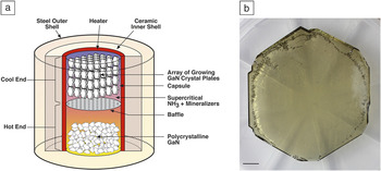
The ammonothermal technique is analogous to the hydrothermal process for the simultaneous growth of many large quartz crystals per run at low cost; thus, it has the potential for becoming the lowest cost route to producing GaN crystals. However, the initial cost is high due primarily to the need for noble metal components and the long learning curve to achieve initial crystals of viable size and purity, and several significant technical hurdles including the very slow growth rate range of 10–30 μm/hr must be surmounted before this achievement is realized. A schematic of the internally heated growth system and a photo of a two-inch diameter crack-free, as-grown bulk crystal are shown in Figure 1a and b, respectively.Reference D’Evelyn, Ehrentraut, Jiang, Kamber, Downey, Pakalapati and Yoo7,Reference Jiang, Ehrentraut, Downey, Kamber, Pakalapati, Yoo and D’Evelyn8 In general, the growth procedure involves the placement of GaN seed crystals in the top of the chamber and the use of a polycrystalline GaN nutrient, a mineralizer having a positive solubility coefficient for GaN (e.g., NH4Cl) and ammonia contained inside a sealed capsule. A heater, a ceramic shell that provides thermal insulation, and an externally cooled steel outer shell for mechanical confinement successively surround the capsule. The operating temperature and pressure ranges are 650–750°C and 100–600 MPa, respectively.Reference D’Evelyn, Hong, Park, Lu, Kaminsky, Melkote, Perlin, Lesczynski, Porowski and Molnar9 The crystals typically are n-type with carrier concentrations in the mid-1016 to mid-1018 cm–3 range and dislocation densities in the 5 × 104 cm–2 to 5 × 106 cm–2 range that is two–four orders of magnitude lower than in HVPE grown crystals (see below). Investigators at Ammono S.A. in Warsaw, Poland, have reportedReference Dwiliński, Doradziński, Garczyński, Sierzputowski, Puchalski, Kanbara, Yagi, Minakuchi and Hayashi10,Reference Dwiliński, Doradziński, Garczyński, Sierzputowski, Kucharski, Zając, Rudziński, Kudrawiec, Serafińczuk and Strupiński11 the ammonothermal growth of polar, non-polar, and semi-polar crystals with diameters of one and two inches and dislocation densities as low as 5 × 103 cm–2.
(a) Schematic of high-pressure ammonothermal crystal growth apparatus employed at Soraa for growth of GaN single crystals (from Reference 7). (b) As-grown nominal two-inch diameter GaN(0001) crystal produced using the ammonothermal method (from Reference 8). Bar = 0.25 in. In this process, either polycrystalline GaN or evaporated Ga and N are dissolved in the solvent mixture of supercritical ammonia and a mineralizer (commonly either NH4Cl or NaNH2) in a hotter region of a sealed container. The saturated solution is transported to the cooler upper zone by convective motion. The solution becomes supersaturated, and deposition of GaN continuously occurs on the small crystals of GaN suspended in the vessel prior to closure.

If the size of the boules and wafers derived from this technique can be substantially increased in the manner of the evolution of the growth of ever-larger quartz crystals, sufficient cost reduction may be realized to meet the increasing need for chemically similar substrates that contain a very low density of dislocations.
At the time of this writing, the HVPE technique coupled with laser-induced liftoff of GaN boules grown on sapphire substrates is the most widely investigated technique and has become a commercial process for a few companies. Wafers derived from boules produced by this method became the substrate of choice for GaN-based lasersReference Uchida, Agatsuma, Hashizu, Yamamoto and Ikeda12 and are currently used by Soraa to grow high-performance GaN-on-GaN light-emitting diodes.Reference Cich, Aldaz, Chakraborty, David, Grundmann, Tyagi, Zhang, Steranka and Krames6
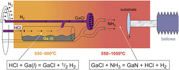
A schematic of an HVPE apparatus and the basic chemistry involved in the growth of GaN boules is shown in Figure 2. At present, the number of useful wafers that can be commonly gleaned from a single boule is in the range of 2–6, as there are multiple challenges in the growth of boules thicker than 10 mm. An example of a GaN boule grown via HVPE that is essentially the state of the art, and the associated crystallography of the edge and top regions is shown in Figure 3. The yield is often low due to crack formation either during growth and/or on cooling or during removal from the sapphire substrate; therefore, the cost of each wafer is very high. These factors coupled with a relatively high density (106–107 cm–2) of threading dislocations that act as vertical current leakage paths and reduce the maximum voltage of vertical devices limit their usefulness for power switches. These factors and the high cost of wafers with a low pinhole density have presently tempered interest in this approach in favor of new and less costly GaN and AlN template films grown on sapphire. Perhaps, ammonothermal growth of low defect density substrates in tandem with subsequent homoepitaxial HVPE of boules from which many wafers can be diced will be the next step in acquiring low defect density bulk GaN boules and wafers with different orientations. An in-depth review of the status and characteristics of GaN substrates grown by this technique and a comparison with other techniques for growth of GaN boules in polar and nonpolar orientations has been published.Reference Paskova and Evans14
Schematic of hydride vapor-phase epitaxy apparatus, process route, and growth chemistry for the growth of GaN crystals. In this process, hot gaseous GaCl is formed by passing hot HCl gas over liquid Ga. The GaCl then reacts with ammonia gas (NH3) to form GaN that deposits and grows on a heated substrate. All reactions are achieved in a temperature controlled quartz furnace. Courtesy D.R. Clarke.

(a) Plan and (b) oblique views of freestanding bulk GaN crystal grown by hydride vapor-phase epitaxy at 1010°C for 55 h with a thickness of 5.8 mm and diameter of 52 mm. Cross-sectional schematic images of the bulk GaN crystal for (c) {11 $\mathop 2\limits^ - $0} and (d) {10
 $\mathop 1\limits^ - $0} planes (from Reference 13). Dashed line in (c) indicates the top of the ∼3 mm distance on the crystal face.

Research on the growth of AlN single crystals has been conducted for decades. Recently, freestanding AlN substrates have been fabricated by sublimation,Reference Miyanaga, Mizuhara, Fujiwara, Shimazu, Nakahata and Kawase15 physical vapor transport (PVT) (sublimation-recombination technique),Reference Kumagai, Yamane and Koukitu16,Reference Dalmau, Moody, Schlesser, Mita, Xie, Feneberg, Neuschl, Thonke, Collazo, Rice, Tweedie and Sitar17 flux methods,Reference Yano, Okamoto, Yap, Yoshimura, Mori and Sasaki18 and solution growth.Reference Kamei, Inoue, Shirai, Tanaka, Okada and Yauchi19 The two most promising techniques are PVT and solution growth. PVT has the advantage of being a simpler process with simpler equipment, with the potential for mass production and lower cost. It involves the sublimation of a sintered polycrystalline AlN platen or AlN powder onto a substrate such as AlN(0001) or SiC(0001) at temperatures up to ∼2300°C in N2 near atmospheric pressure. The process is commonly conducted in a refractory container such as tungsten. The distance between the AlN and the substrate varies between being directly adjacent and ≥10 cm. Growth rates normally range from 150–170 μm/hr, which is slow and will keep the retail cost per wafer high. The dislocation density in material grown on AlN crystals is often non-uniform and in the range of 102–105 cm−2. The grown crystals are commonly amber colored because of the deficiency of nitrogen. This will be a problem for the transmission of ultraviolet light from light-emitting diodes and lasers. The material grown on SiC commonly contains microcracks, which form on cooling due to the mismatch in the coefficients of thermal expansion between the AlN crystal and the substrate.
The solution growth method currently takes two forms. Materials may be grown in refractory carbide crucibles at temperatures as high as 2200°C; however, the as-grown materials are usually contaminated with C and other elements due to out diffusion from the crucible. The slow cooling in a thermal gradient from 1600°C of a molten Cu66Al31Ti3 alloy solvent contained in a carbon crucible containing a SiC(0001) seed has been used in various ways to grow AlN films with a thickness of several micrometers.Reference Kamei, Inoue, Shirai, Tanaka, Okada and Yauchi19 The initial application of AlN substrates has been primarily for ultraviolet optoelectronic devices.Reference Grandusky, Chen, Gibb, Mendrick, Moe, Rodak, Garrett, Wraback and Schowalter20 However, high-power and high-frequency devices will certainly be produced and characterized in the near future as the demand for these devices continues to grow.
Homoepitaxy of GaN and related films
Informative literature regarding the historical and current techniques and process routes that have been and are being used for the growth of Group III-nitride-based thin films and device structures have been published.Reference Strite, Lin and Morkoç21–Reference Davis, Bhattacharya, Fornari and Kamimura27 The following paragraphs briefly review the precursor chemistry, process procedures, and results obtained using organometallic vapor-phase epitaxy (OMVPE) for the growth of Group III-nitride thin films, as this is the commercially employed technique for this purpose. Note that the technique is also referred to as metalorganic chemical-vapor deposition.
The growth of thin films of Group III nitrides by OMVPE involves the gas phase transport of (a) vapors of organometallic liquid and solid precursors and associated carrier gases into the reactor chamber, (b) hydrides containing nitrogen, and (c) diluent gases including H2 and N2. The diluent gases prevent pyrolysis of the gas phase precursors prior to the precursors reaching the heated substrate. On the substrate, the reactants decompose and then the reaction products combine to grow the desired film.
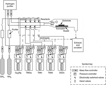
A schematic of a commonly configured OMVPE growth system is shown in Figure 4.Reference DenBaars, Keller, Pancove and Moustakas23The most common Group III organometallic sources are either liquids including trimethylaluminum (TMAl) ((CH3)3Al), trimethygallium (TMGa) ((CH3)3Ga), triethylgallium (TEGa) ((C2H5)3Ga), or solids such as trimethylindium (TMIn) ((CH3)3In). The stability of these molecules decreases from Al to Ga and to In. Thus, TMAl and TMIn are the most and least stable molecules, respectively. The ethyl radicals have a much lower reactivity than the methyl radicals. As such, the latter are a source of C incorporation into the nitride films during growth. The Al-containing precursors are also extremely reactive with C and O2, the latter commonly derived from the quartz walls of the reaction chamber and/or reaction with the OH– radical in H2O. This is the principal reason that significant oxygen concentrations are present in Al-containing nitride films. The bond dissociation energy of the triple bond of the dimer N2 molecule is 945 kJ/mole; thus, the molecule has very high thermal stability and can only be effectively used as a precursor for the deposition of AlN films above 1600°C. For OMVPE of this compound and all other III-nitride films within the normal growth temperature range from 600°C to 1100°C, the most common approach is to use ammonia (NH3). The common donor and acceptor dopant sources are the Si-containing hydride gases (SiH4 and Si2H4) diluted in H2 and the organometallic solid of bis-cyclopentadienylmagnesium (Cp2Mg), respectively. The metals contained in these dopants enhance the electronic conductivity of the nitride films and the solid solutions made from the binary compounds.
Schematic of horizontal-type inductively heated organometallic vapor-phase epitaxy reactor for the deposition of Group III-nitride thin films and device heterostructures (from Reference 23). In this process, the vapors of the metalorganic (MO; referred to in the text as organometallic) sources become entrained in hydrogen flowing through each of the bottles at the bottom of the figure, flow to the deposition chamber, mix with the ammonia, and undergo decomposition and reaction with each other on a substrate to form a Group III-Nitride film. Note: Cp2Mg, bis-cyclopentadienylmagnesium; TMAl, trimethylaluminum; TMGa, trimethygallium; TMIn, trimethylindium; DEZn, diethylzinc.

The organometallic sources are contained in the temperature-controlled bubblers shown in Figure 4 through which a carrier gas (H2 for TMGa, TEGa, and TMAl, and N2 for TMIn) is flowed to entrain the vapor of each of these species and transport it into the growth chamber and onto the heated substrate contained within. The substrates are normally seated on or recessed into a sample platter that has been purified in a Cl atmosphere at 2100°C to remove residual metals and coated with very high purity SiC to prevent C incorporation into the growing film. The sample platter rests on a graphite disk, which is heated either resistively or via the magnetic field produced in a water-cooled coil connected to a RF generator and either surrounding the chamber or residing underneath the graphite disk. Decomposition of the organometallic sources occurs via endothermic reactions (i.e., the input of heat induces this reaction). As such, the sidewall of the growth chamber is commonly an annulus composed of two concentric quartz walls between which cold water is flowed to prevent these reactions that would coat the inside wall and cause a change in the temperature of the substrate.
Thermodynamic analysis of the equilibrium dissociation rate of ammonia via the reaction
 $$N{H_{3\,}} = 1/2{N_2} + 3/2{H_2}$$
indicates that the hydride should be fully decomposed even at temperatures as low as 400°C. However, the kinetics of this reaction are sufficiently slow that the equilibrium state is never even approached in practice. In fact, only a small fraction (≤ 4%) of the ammonia is decomposed up to 950°C. The equilibrium N2 pressure over GaN for example is hundreds of atmospheres under the growth conditions commonly used in OMVPE, and decomposition of GaN into gaseous N2 and Ga droplets on the growth surface according to the reaction
 $$GaN = Ga(1) + 1/2{N_2}$$
would occur if this were the reactant source of nitrogen. However, the conditions commonly obtained in an OMVPE reactor are described by the combination of Equations 1 and 2, namely,
 $$N{H_3} + Ga(1) = GaN + 3/2{H_2}.$$
This equation describes the stabilization of the GaN surface via the reaction of liquid Ga with ammonia to continually form solid GaN. In other words, the presence and decomposition of ammonia is preventing the decomposition of the GaN surface.
In practice, significant partial pressures of ammonia are required to stabilize the surface for all nitrides, especially GaN, InN and solid solutions of these compounds. The growth of Group III-nitride films is commonly conducted using high Group V(NH3)/Group III (e.g., TEGa) ratios (e.g., ≥2000:1). As such, the formation of intermediate adducts in the gas phase between Group III and Group V precursors is likely even when they are diluted with H2 or a N2 diluent in the reactor. The formation of a strong adduct can readily occur because the Group III organometallic species are electron acceptors (Lewis acids) and ammonia is an electron donor (Lewis base). For example, the growth of AlN from a mixture of TMAl and NH3 is believed to occur by the initial formation of the intermediate gas phase adduct compound, trimethylaliummonamine (CH3)3Al:NH3, followed by the elimination of one methane (CH4) molecule near the surface of the hot substrate.
Surface chemistry studies using Fourier transform infrared and x-ray photoelectron spectroscopy of mixtures of TMAl and NH3 adsorbed on Al2O3 at room temperature revealed the co-adsorption of (CH3)3Al and NH3 and the formation of a surface adduct species (CH3)2AlNH3 together with adsorbed NH3.Reference Liu, Bertolet and Rogers28 Raising the substrate temperature above 320°C caused the appearance of vibrational bands corresponding to AlN and indicated the emergence of extended (Al–N) networks in the form of Al(NH2)2Al species. Molecular hydrogen was eventually eliminated from these molecules to yield AlN.
As noted above, H2 is used as a diluent gas for transporting the reactants to the substrate surface during the growth of Al- and Ga-containing Group III-nitride films. The presence of hydrogen, especially in the atomic state derived primarily from the sequential decomposition of NH3, can lead to significant etching of all nitride films at the temperatures of growth and above and can affect the growth rate and microstructural character of the deposited films. This is especially true for films containing In, as its incorporation is readily reduced when H2 is used as the diluent. As such, N2 is the diluent of choice in the growth of In-containing films.
Summary
Recent progress in the development and employment of different techniques for the growth of GaN and AlN substrates for the growth of GaN-based lateral and vertical power device heterostructures has been presented. The nature and use of organometallic precursors and ammonia reactants as well as the diluents commonly used for the growth of thin films and device structures on these and other substrates have also been discussed. To become competitive with silicon devices, OMVPE grown, Group III-Group V power structures on Group III-nitride substrates will require higher yields of larger diameter wafers at a lower cost. Slow but steady progress has been made along several growth routes; however, all current processes are challenging in that the dislocations densities in the thin film and device products remain high, the growth of substrates for homoepitaxial deposition of films is slow and expensive, and device yield with the desired properties remains low. Much more remains to be achieved.