Introduction
A perovskite with a chemical formula of ABX3 is a crystal structure having corner-sharing octahedral AX6 and face-sharing cubo-octahedral BX12. The organometal halide RMX3 (R = methylammonium or foramidnium, M = Pb or Sn, X = Cl, Br, I, or mixed halide) is a key material for perovskite solar cells (see the Introductory article in this issue of MRS Bulletin). Three-dimensional (3D) lead and tin methylammonium halides were first reported in 1978, Reference Weber1,Reference Weber2 where their color changed from colorless to black as the halide would change from chloride to iodide due to a decrease in the bandgap. Layered 2D organotin halides were reported to show an insulator-metal transition when modulating the number of inorganic layers in the (C4H9NH3)2(CH3NH3) n–1Sn n I3n+1 perovskite, Reference Mitzi, Feild, Harrison and Guloy3 which received attention because high-temperature superconducting properties were possible from organic–inorganic perovskite materials.
Contrary to the 2D materials, little attention has been paid to the photovoltaic ability of 3D organic–inorganic halide perovskite materials due to their poor optoelectronic properties. In 2009, the Miyasaka group first used MAPbI3 (MA = CH3NH3) as an inorganic sensitizer in dye-sensitized liquid junction-type solar cells, Reference Kojima, Teshima, Shirai and Miyasaka4 yielding a power-conversion efficiency (PCE) of ∼4%. However, this paper was not cited for two years because it reported a much lower PCE as compared with ruthenium-based dyes, which was the most commonly used molecular-type sensitizer in dye-sensitized liquid-type solar cells.
In 2011, Park’s group reported a MAPbI3 perovskite-sensitized solar cell with an improved efficiency of 6.5%. Reference Im, Lee, Lee, Park and Park5 Although their report described more advanced technology for higher efficiency through the utilization of a spin-coating method using an optimized precursor solution, this result was not cited until the development of a long-term stable perovskite solar cell in 2012 by Park’s group, Reference Kim, Lee, Im, Lee, Moehl, Marchioro, Moon, Humphry-Baker, Yum, Moser, Grätzel and Park6 overcoming the instability of MAPbI3 in a polar liquid electrolyte. Research on perovskite solar cells has been triggered by the discovery of the long-term durable solid-state perovskite solar cell. Reference Kim, Lee, Im, Lee, Moehl, Marchioro, Moon, Humphry-Baker, Yum, Moser, Grätzel and Park6 The number of research papers related to perovskite solar cells has changed from 1 in 2009, 1 in 2011, 4 in 2012, and 56 in 2013, to 460 in 2014.
As a result of subsequent intensive research, the National Renewable Energy Laboratory certified a PCE of 20.1%, fabricated by the Korea Research Institute of Chemical Technology, at the end of 2014. 7 Such a high photovoltaic performance is mainly attributed to high-quality MAPbI3 material, whose quality depends significantly on the fabrication method used. MAPbI3 can be prepared by either a one-step spin-coating procedure or a sequential two-step deposition technique. The morphology and optoelectronic properties were found to be better controlled by a two-step method. In this article, two-step deposition technologies for high-efficiency perovskite solar cells are described in detail.
Device structure
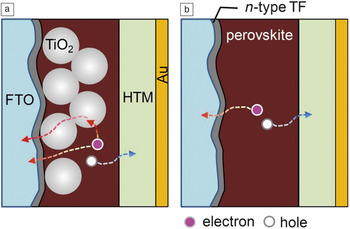
Perovskites were initially used as a sensitizer in the dye-sensitized solid-state solar cell structure, in which photogenerated electrons in the perovskite were injected into TiO2. The balanced electron and hole diffusion lengths observed in MAPbI3 Reference Xing, Mathews, Sun, Lim, Lam, Grätzel, Mhaislkar and Sum8,Reference Stranks, Eperon, Grancini, Menelaou, Alcocer, Leijtens, Herz, Petrozza and Snaith9 allow this material to be used in a p-n or p-i-n junction structure, for which a mesoscopic nanostructure ( Figure 1a) and a planar structure (Figure 1b) have been studied. Both structures contain a thin compact TiO2 layer, but the mesoscopic structure possesses a mesoporous oxide layer.
(a) Mesoscopic perovskite solar cell employing a mesoporous TiO2 layer and (b) planar structure without a mesoporous oxide layer. The thin film (TF) on fluorine-doped tin oxide (FTO) is an electron collecting n-type semiconductor. HTM represents hole transporting material. Flows of an electron and a hole are represented by arrows. Reprinted with permission from Reference 10. © 2015 Wiley.

In the mesoscopic structure, sometimes a perovskite capping layer forms on the mesoporous oxide layer. Therefore, in contrast to the planar structure, the mesoscopic structure has two different morphologies: the nanocrystalline perovskite formed in the pores of the oxide film and the bulk perovskite formed in the capping layer. There is no doubt that the perovskite provides electron and hole pathways in the planar structure, whereas electrons can be transported both in the oxide layer and in the perovskite layer for the mesoscopic structure. It should be noted that although the working mechanism might be different depending on the device structure, the photovoltaic performance is mainly dependent on the quality of the perovskite regardless of the device structure.
Perovskite fabrication methods
Solution process: One-step versus two-step coating
MAPbI3 can be readily formed by a solution process via a spin-coating technique. Two procedures have been proposed—one-step and two-step deposition methods. For one-step spin-coating, a precursor solution is prepared by mixing MAI (or MACl) and PbI2 in polar aprotic solvents such as N,N-dimethylformamide (DMF) or gamma-butyrolactone (GBL). Reference Kojima, Teshima, Shirai and Miyasaka4–Reference Kim, Lee, Im, Lee, Moehl, Marchioro, Moon, Humphry-Baker, Yum, Moser, Grätzel and Park6,Reference Lee, Teuscher, Miyasaka, Murakami and Snaith11 Spin-coating of the precursor solution is followed by drying and heating at mild temperatures (70°C∼170°C), where the spinning rate, drying process, and temperature are expected to affect the MAPbI3 morphology.
Mitzi’s group first proposed sequential two-step coating for overcoming difficulties with morphology control and choice of solvent involved with the one-step spin-coating technique in 1988. Reference Liang, Mitzi and Prikas12 A PbI2 film was first deposited on a substrate using vacuum evaporation or spin coating, either of which was followed by dipping in a MAI solution to form MAPbI3. Grätzel’s group used this technique for perovskite solar cells, where the dipping time and concentration of the PbI2 precursor solution were found to affect photovoltaic performance. Reference Burschka, Pellet, Moon, Humphry-Baker, Gao, Nazeeruddin and Grätzel13 A modified two-step coating method without the dipping process was proposed, where the PbI2 solution was first coated on the substrate to form a layered PbI2 film, and then the 2-propanol solution of CH3NH3I was spun onto the TiO2 film. Reference Im, Kim and Park14,Reference Im, Jang, Pellet, Grätzel and Park15 Figure 2 shows schematics of the procedures for the one-step and two-step spin-coating methods. In the case of using a single solvent such as DMF or N,N-dimethylacetamide (DMA), one-step spin coating (average PCE = 7.5%) was found to be inferior to two-step spin coating (average PCE = 13.9%) in terms of photovoltaic performance due to significant differences in the morphology of MAPbI3. Reference Im, Kim and Park14
One-step and two-step coating procedures to deposit MAPbI3 perovskite films. The one-step coating procedure was conducted using a single precursor solution containing MAI (CH3NH3I) and PbI2, while the two-step coating method was performed by reacting the spin-coated PbI2 film with the MAI solution. DMA, DMF, and IPA represent N,N-dimethylacetamide, N,N-dimethylformamide, and isopropyl alcohol, respectively. Reprinted with permission from Reference 14. © 2014 AIP Publishing. Note: MA, CH3NH3.

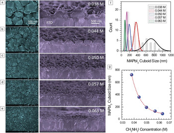
The crystal size of the perovskite can be readily controlled by the two-step spin-coating method. In this procedure, the size of MAPbI3 was found to be significantly altered by the concentration of MAI in the second step of spin coating. Reference Im, Jang, Pellet, Grätzel and Park15 Crystal size increased as the MAI concentration decreased, for instance, a 38 mM solution produced 700 nm-sized MAPbI3 crystals, but a 63 mM solution yielded a smaller size of approximately 90 nm, as seen in Figure 3 . The shape of MAPbI3 crystal was cuboid, irrespective of the MAI concentration.
(a–e) Plan-view and cross-sectional scanning electron microscopy images of MAPbI3 crystals, (f) size distribution (solid line indicates Gaussian distribution fitting), and (g) size of MAPbI3 cuboids depend on MAI (CH3NH3I) concentration. All the images in the respective columns were taken at the same magnification. The size of the MAPbI3 cuboid crystal increases for decreasing MAI concentration. Reprinted with permission from Reference 15. © 2014 Nature Publishing Group. Note: MA, CH3NH3; FTO, fluorine-doped tin oxide.

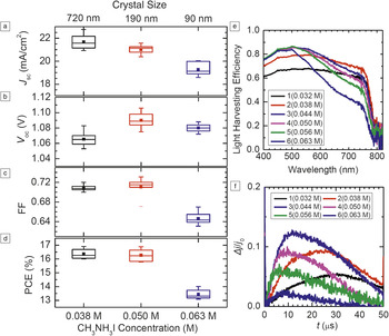
Besides morphological control by two-step spin coating via MAI concentration change, it is also important to note that photovoltaic performance is strongly influenced by the MAPbI3 size. Figure 4a–d compares photovoltaic parameters with respect to the MAPbI3 size. Reference Im, Jang, Pellet, Grätzel and Park15 Photocurrent density increased with increasing MAPbI3 size, while the photovoltage was the highest at an intermediate size of about 200 nm. Fill factor generally becomes higher with increasing MAPbI3 size. It was found that the increasing photocurrent with increasing size could be ascribed to the improved light harvesting efficiency, as can be seen in Figure 4e, as well as better charge extraction ability, as confirmed by photo-CELIV (photogeneration and carrier extraction by linearly increasing the voltage) in Figure 4f, in which photo-CELIV measured hole carrier extraction by linearly increasing the voltage under illumination using FTO/bl-Al2O3/mp-TiO2/MAPbI3/spiro-OMeTAD/Au assemblies (FTO = fluorine-doped tin oxide; bl = blocking layer; mp = mesoporous; spiro-OMeTAD = 2,2′,7,7′-tetrakis(N,N-di-p-methoxyphenylamine)-9,9-spirobifluorene). However, considering Δj/j 0 (Δj = extraction current, j 0 = capacitive displacement current) is proportional to the hole mobility, a slightly lower photovoltage for a crystal size of 700 nm is probably related to retarded hole mobility compared to the smaller crystals, as can be seen in Figure 4f, because slow hole mobility is likely to increase recombination. To attain high photovoltage along with high photocurrent and fill factor, it is necessary to manipulate the crystal size to yield fast mobility in order to minimize recombination and high charge extraction and light scattering to maximize the photocurrent.
Effect of MAI (CH3NH3I) concentration on (a) short-circuit current density (J sc), (b) open-circuit voltage (V oc), (c) fill factor (FF), (d) power-conversion efficiency (PCE), (e) light harvesting efficiency, and (f) photo-CELIV (charge extraction by linearly increasing voltage) transients. For each data point, the bottoms and tops of boxes indicate first and third quartiles, respectively. The PCE increases with decreasing MAI concentration. Light harvesting efficiency increases with decreasing MAI concentration until 0.032 M, while charge extraction becomes faster with increasing MAI concentration. In photo-CELIV spectra, the rise time of the Δj/j 0 curve is inversely proportional to the charge extraction rate, and the area under the curve corresponds to the total amount of extracted charge. The device configuration was FTO/bl-TiO2/mp-TiO2/MAPbI3/spiro-OMeTAD/Au for J–V measurements and FTO/bl-Al2O3/mp-TiO2/MAPbI3/spiro-OMeTAD/Au for the photo-CELIV study. Reprinted with permission from Reference 15. © 2014 Nature Publishing Group. Note: MA, CH3NH3; t, time; Δj, extraction current; j 0, capacitive displacement current; FTO, fluorine-doped tin oxide; bl, blocking layer; mp, mesoporous; spiro-OMeTAD, 2,2′,7,7′-tetrakis(N,N-di-p-methoxyphenylamine)-9,9-spirobifluorene.

Vacuum process
Perovskite films can also be prepared by the thermal evaporation method. Co-evaporation of MAI and PbCl2 led to a MAPbI3 phase, and uniformity of the film was much better than the solution-processed film. Reference Liu, Johnston and Snaith16 Since vacuum deposition uses two chemical sources, it can be regarded as a two-step coating process in a sense. Thus, MAI can be also deposited onto the PbI2 film by evaporation.
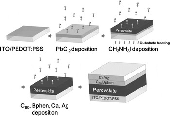
A vapor-assisted solution process was proposed to grow perovskite films via the in situ reaction of an as-deposited film of PbI2 with MAI. Reference Chen, Zhou, Hong, Luo, Duan, Wang, Liu, Li and Yang17 The perovskite film prepared by this method showed a well-defined grain structure with grain size up to the microscale, full surface coverage, and small surface roughness. A sequential two-step vacuum deposition method ( Figure 5 ) was applied to prepare planar structured perovskite solar cells, Reference Chen, Kang, Hsiao, Yang, Chiang and Lin18 where MAI was evaporated after PbCl2 evaporation onto an indium-doped tin oxide/poly(3,4-ethylenedioxythiophene) poly(styrene sulfonate)(ITO/PEDOT:PSS) substrate. In this process, the substrate was heated while depositing MAI vapor, and the substrate temperature was found to be critical for photovoltaic performance. For example, photovoltaic performance was better when the substrate was heated to 75°C compared to a substrate temperature of 65°C or 85°C.
Sequential two-step vacuum deposition using PbCl2 and MAI to fabricate a planar-structured perovskite solar cell. MAI (CH3NH3I) was evaporated onto a pre-evaporated PbCl2 film while the substrate was heated. Reprinted with permission from Reference 18. © 2014 Wiley. Note: ITO, indium tin oxide; PEDOT:PSS, poly(3,4-ethylenedioxythiophene):poly(styrene sulfonate); Bphen, Bathophenanthroline; MA, CH3NH3.

Two-step deposition of HC(NH2)2PbI3 (FAPbI3)
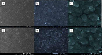
Although MAPbI3 exhibits superb photovoltaic performance, there are issues to be addressed, including the tetragonal–cubic phase transition at approximately 56°C. Reference Baikie, Fang, Kadro, Schreyer, Wei, Mhaisalkar, Grätzel and White19 This temperature is critical when taking into consideration the solar cell operates at temperatures up to 85°C. The band structure of MAPbI3 can be affected by the phase transition, which also has a negative influence on photovoltaic performance. HC(NH2)2PbI3 (FAPbI3) is an alternative to MAPbI3 because FAPbI3 is free from such a phase transition. FAPbI3 can be formed by a two-step deposition process, where the spin-coated PbI2 film is dipped in a HC(NH2)2I (FAI) solution, followed by a heat treatment at 150°C. Reference Lee, Seol, Cho and Park20 Similarly, FAPbI3 crystals were fabricated by a two-step deposition procedure, where the morphology was less influenced by the substrate. Figure 6 shows a similar FAPbI3 morphology regardless of the substrate type: with and without a compact TiO2 film.
Plan-view scanning electron microscopy images of FAPbI3 coated on (a–c) the compact TiO2 layer (planar structure without mesoporous TiO2 layer) and (d–f) the mesoporous TiO2 layer (mesoscopic structure). The scale bars on left, middle, and right images represent 1 µm, 1 µm, and 100 nm, respectively. Reprinted with permission from Reference 20. © 2014 Wiley. Note: FA, HC(NH2)2.

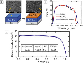
Fabricating an ultrathin layer of MAPbI3 on a FAPbI3 surface ( Figure 7a) compensates for pin holes formed on the FAPbI3 film surface and additionally increases the incident photon-to-electron conversion efficiency (or incident photon-to-current conversion efficiency) at the optical bandgap absorption, as indicated by the black arrow in Figure 7b. FAPbI3 formed by two-step deposition demonstrates a PCE of 16% and shows better photostability compared to two-step spin-coated MAPbI3.
(a) Plan-view scanning electron microscopy images of the FAPbI3 layer with and without the ultrathin MAPbI3 layer. Scale bars indicate 1 μm. (b) Incident photon-to-electron efficiency (IPCE) spectra of perovskite solar cells based on FAPbI3, MAPbI3, and FAPbI3 with thin MAPbI3, where the integrated J sc was calculated to be 19.57, 18.90, and 20.22 mA/cm2, respectively. (c) Current–voltage curve of the best performance FAPbI3 perovskite solar cell. J SC improved due to increased band-edge absorption after formation of a thin MAPbI3 layer on top of FAPbI3, as indicated by the black arrow in (b), which resulted in a PCE of 16.01%. Reprinted with permission from Reference 20. © 2014 Wiley. Note: FA, HC(NH2)2; MA, CH3NH3; FF, fill factor; J sc, short-circuit current density; V oc, open-circuit voltage; PCE, power-conversion efficiency.

Summary
A two-step deposition procedure was described to fabricate a RPbI3 (R = CH3NH3 or HC(NH2)2) perovskite layer on a substrate with and without a mesoporous TiO2 film. MAPbI3 could be formed by either dipping or spin coating the PbI2 film, where crystal size was controlled by varying the MAI concentration. The MAPbI3 crystal size significantly influenced photovoltaic performance. Instead of using the MAI solution, MAI could be evaporated onto the PbI2 film to form MAPbI3, which is expected to regulate MAPbI3 layer thickness and surface roughness. The evaporation method will be more beneficial for a tandem architecture. Although high photovoltaic performance was realized by the two-step spin-coating method, further efforts need to be devoted to developing a facile method for large-area coating to help facilitate scaling up the process.
Acknowledgments
This work was supported by National Research Foundation (NRF) of Korea grants funded by the Ministry of Science, ICT & Future Planning (MSIP) of Korea under contracts No. NRF-2012M1A2A2671721, 2012M3A7B4049986 (Nano Material Technology Development Program), and NRF-2012M3A6A7054861 (Global Frontier R&D Program on Center for Multiscale Energy System).