Introduction
An impedance transformer is one of the most important components widely used in radio frequency and microwave fields to match the impedance differences between different circuits or systems to achieve highly efficient signal transmission and maximum power transmission. Impedance transformers can be applied to power divider, couplers, antennas, filters, mixer, power amplifiers, and low noise amplifiers [Reference Roshani, Dehghani and Roshani1–Reference Wong, Arslan and Erdogan8]. There are many ways to realize multi-band components. A novel approach for designing dual-mode dual-band bandpass filters is proposed in [Reference Sung9]. They realize it by embedding a pair of slits in the square patch, and one transmission zero is introduced between the two passbands. An exact synthesis and design procedure is proposed in [Reference Zhang and Zhu10], which gives a class of wideband dual-band bandpass filters that can achieve both controllable in-band ripple factor and isolation between the dual passband. A mixed transmission zero embedded dual-band impedance transformer that operates at two uncorrelated frequencies in Chuang et al. [Reference Chuang, Wu, Tsai and Chang11] is presented. By deploying the cross-shaped structure, an impedance transformer that can significantly eliminate the line width limitation of traditional quarter-wave impedance transformer is proposed in Zhu et al. [Reference Zhu, Cheong, Ho, Tam and Choi12]. A novel design of ultra-wideband impedance transformers and power dividers with filtering capabilities is given in Cao et al. [Reference Cao, Liu, Liang and Majid13]. A design of an impedance transformer with wideband, maximally flat real-to-real impedance matching is proposed in Darraji et al. [Reference Darraji, Honari, Mirzavand, Ghannouchi and Mousavi14], with exact solutions for transmission lines’ parameters being derived in explicit form for any impedance transformation ratio being given.
With the development of complexity and miniaturization of device functions, the demand for components that meet the use of multiple frequency bands is increasing. A three-section transmission line transformer is proposed in Jones [Reference Chongcheawchamnan, Patisang, Srisathit, Phromloungsri and Bunnjaweht15], which can match real impedance at three arbitrary frequencies between assigned frequency  ${f_0}$ and its third harmonic. Then, a compact quad-frequency impedance transformer with a two-section coupled line is proposed in Schiek and Kohler [Reference Bai, Wang, Gao, Huang and Shi16], which can achieve an ideal impedance matching at four frequencies. To match a load at three arbitrary frequencies, a compact tri-band impedance transformer by utilizing stubbed coupled line is proposed in Chongcheawchamnan et al. [Reference Wang, Zhang, Xu, Bai, Liu and Shi17].
A novel type of transformer to match real impedance load at four frequencies is proposed in this paper. The transformer is composed of two sections of stubbed coupled line. We changed the short-circuit form in Chongcheawchamnan et al. [Reference Wang, Zhang, Xu, Bai, Liu and Shi17] into an open-circuit form to reduce the number of grounding holes and simplify the structure of impedance transformer, so the loss of manufacture could be reduced. In this paper, we derive and analyze the design equations carefully. In addition, we also deduce the range of frequency ratios analytically and numerically. We evaluated several cases to certify it is feasible and valid to realize impedance matching theoretically at four different frequencies. We choose the transformer’s working frequencies at 0.7/2.4/3.6/5.3 GHz to verify the validity of the proposed impedance transformer in the application. After fabricating and measuring, it turns out that the simulated results are in good agreement with the measured results.
Structure and design
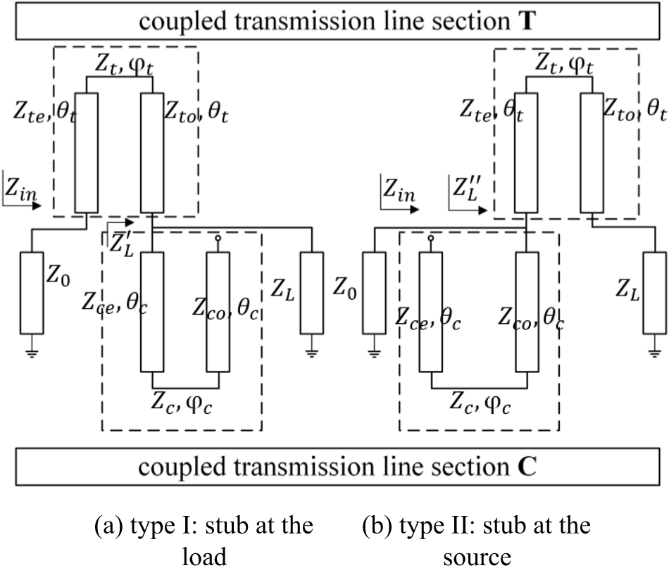
Figure 1 shows that the circuit structure of the proposed quad-band impedance transformer is simply composed of two sections of coupled line sections T and C, and section C is an open-circuit form. Section T is the coupled transmission line, and section C is the stubbed coupled line, respectively, in Figure 1(a) and Figure 1(b). The structures of two types are shown in Figure 1(a) and Figure 1(b).
Structure of the proposed quad-band transformer. (a) Type I: stub at the load. (b) Type II: stub at the source.

As shown in Figure 1, the odd and even mode characteristic impedances of T and C coupled transmission lines are  ${Z_{to}}$,
 ${Z_{te}}$,
 ${Z_{co}}$, and
 ${Z_{ce}}$ and the image impedance of T and C are
 ${Z_t}$,
 ${Z_c}$. The
 ${\varphi _t}$ and
 ${\varphi _c}$ are insert phases of the coupled transmission line sections T and C. With the equal electrical lengths
 ${\theta _t}$ and
 ${\theta _c}$ of the two modes, the odd and even modes, it is set to the same odd and even mode impedance ratio
 $\rho $
 $\left( {\rho \gt 1} \right)$ for transmission lines according to Jones’ theory in Bai et al. [Reference Jones18], so we can give the following equations:
 \begin{equation}\begin{array}{*{20}{c}}
{{Z_t} = \sqrt {{Z_{te}} \cdot {Z_{to}}} }
\end{array}\end{equation}
 \begin{equation}\begin{array}{*{20}{c}}
{{Z_c} = \sqrt {{Z_{ce}} \cdot {Z_{co}}} }
\end{array}\end{equation}
 \begin{equation}\begin{array}{*{20}{c}}
{\frac{{{Z_{te}}}}{{{Z_{to}}}} = \frac{{{Z_{ce}}}}{{{Z_{co}}}} = \rho }
\end{array}\end{equation}
 \begin{equation}\begin{array}{*{20}{c}}
{\cos {\varphi _t} = \frac{{\rho - {{\tan }^2}{\theta _t}}}{{\rho + {{\tan }^2}{\theta _t}}}}
\end{array}\end{equation}
 \begin{equation}\begin{array}{*{20}{c}}
{\cos {\varphi _c} = \frac{{\rho - {{\tan }^2}{\theta _c}}}{{\rho + {{\tan }^2}{\theta _c}}}}
\end{array}\end{equation}
The ratio parameter of the impedance transformer between source impedance and load impedance is defined as follows.
 \begin{equation}\begin{array}{*{20}{c}}
{K = \frac{{{Z_0}}}{{{Z_L}}} = \frac{{{Z_{in}}}}{{{Z_L}}}}
\end{array}\end{equation}
Type I: coupled line shunted at the load
We can give the input impedance  ${Z_{in}}$ of the two-section line according to the transmission line theory, as in the circuit structure shown in Figure 1(a).
 \begin{equation}\begin{array}{*{20}{c}}
{{Z_{in}} = {Z_t}\frac{{Z_L^{\text{'}} + j{Z_t}\tan {\varphi _t}}}{{{Z_t} + jZ_L^{\text{'}}\tan {\varphi _t}}}}
\end{array}\end{equation}
 \begin{equation}\begin{array}{*{20}{c}}
{Z_L^{\text{'}} = \frac{{\frac{{{Z_c}}}{{j\tan {\varphi _c}}} \cdot {Z_L}}}{{\frac{{{Z_c}}}{{j\tan {\varphi _c}}} + {Z_L}}}}
\end{array}\end{equation}
Substitute (8) into (7) and observe the real part and the imaginary part, respectively, we can get the following equations:
 \begin{equation}\begin{array}{*{20}{c}}
{\left\{ {\begin{array}{*{20}{c}}
{{Z_{in}}{Z_t}{Z_c} = {Z_t}{Z_c}{Z_L} - Z_t^2{Z_L}\tan {\varphi _c}\tan {\varphi _t}} \\
{j{Z_{in}}{Z_t}{Z_L}\tan {\varphi _c} + j{Z_{in}}{Z_c}{Z_L}\tan {\varphi _t} = jZ_t^2{Z_c}\tan {\varphi _t}}
\end{array}} \right.}
\end{array}\end{equation}
Equation (9) can be written as follows:
 \begin{equation}\begin{array}{*{20}{c}}
{\left\{ {\begin{array}{*{20}{c}}
{\tan {\varphi _c}\tan {\varphi _t} = \frac{{{Z_c}{Z_L} - {Z_{in}}{Z_c}}}{{{Z_t}{Z_L}}}} \\
{\frac{{\tan {\varphi _c}}}{{\tan {\varphi _t}}} = \frac{{Z_t^2{Z_c} - {Z_{in}}{Z_c}{Z_L}}}{{{Z_{in}}{Z_t}{Z_L}}}}
\end{array}} \right.}
\end{array}\end{equation}
Then, to simply the derivation process, let  ${\theta _t} = {\theta _c} = \theta $, therefore
 ${\varphi _t} = {\varphi _c} = \varphi $, and we can rewrite (9) in the following form:
 \begin{equation}\begin{array}{*{20}{c}}
{\left\{ {\begin{array}{*{20}{c}}
{{{\tan }^2}\varphi = \frac{{{Z_c}{Z_L} - {Z_{in}}{Z_c}}}{{{Z_t}{Z_L}}}} \\
{1 = \frac{{Z_t^2{Z_c} - {Z_{in}}{Z_c}{Z_L}}}{{{Z_{in}}{Z_t}{Z_L}}}}
\end{array}} \right.}
\end{array}\end{equation}
Let  $\alpha \equiv {\tan ^2}\varphi $. By solving (11), the following equation is derived:
 \begin{equation}\begin{array}{*{20}{c}}
{\left\{ {\begin{array}{*{20}{c}}
{{Z_t} = \sqrt {{Z_{in}}{Z_L} - \frac{{{Z_{in}}\left( {{Z_{in}} - {Z_L}} \right)}}{\alpha }} } \\
{{Z_c} = \frac{{\alpha {Z_t}{Z_L}}}{{{Z_L} - {Z_{in}}}}}
\end{array}} \right.}
\end{array}\end{equation}
Together with (4), (5), and (11), we can obtain:
 \begin{equation}\begin{array}{*{20}{c}}
{\left\{ {\begin{array}{*{20}{c}}
{\alpha = {{\tan }^2}\varphi } \\
{{{\tan }^2}\theta = \rho \frac{{1 - \cos \varphi }}{{1 + \cos \varphi }} = \rho {{\tan }^2}\frac{\varphi }{2}}
\end{array}} \right.}
\end{array}\end{equation}
We can obtain an expression about  $\theta $ by solving the equations above.
 \begin{equation}\begin{array}{*{20}{c}}
{\theta = m\pi \pm \arctan \left( {\sqrt \rho \tan \frac{{n\pi \pm \arctan \sqrt \alpha }}{2}} \right)}
\end{array}\end{equation}
Both  $m$ and
 $n$ are arbitrary integers, so we can get four unrelated solutions for
 $\theta $ from (14). Since
 $\theta \gt 0$ and a small size impedance transformer is what we want to realize. Therefore, (+) sign is chosen in (14) when
 $m = n = 0$ and (−) sign is chosen in (14) when
 $m = n = 1$. Considering the generality, we assume that
 ${f_1} \lt {f_2} \lt {f_3} \lt {f_4}$, and we can obtain the four fundamental solutions about
 $\theta $ from (14).
 \begin{equation}\begin{array}{*{20}{c}}
{\left\{ {\begin{array}{*{20}{c}}
{{\theta _1} = \arctan (\sqrt \rho \tan \frac{{\arctan \sqrt \alpha }}{2})} \\
{{\theta _2} = \arctan (\sqrt \rho \tan \frac{{\pi - \arctan \sqrt \alpha }}{2})} \\
{{\theta _3} = \pi - \arctan (\sqrt \rho \tan \frac{{\pi - \arctan \sqrt \alpha }}{2})} \\
{{\theta _4} = \pi - \arctan (\sqrt \rho \tan \frac{{\arctan \sqrt \alpha }}{2})}
\end{array}} \right.}
\end{array}\end{equation}
This means the impedance transformer can perfectly match impedance at four different frequencies. Furthermore, assuming  $0 \lt {\theta _1} \lt {\theta _2} \lt {\theta _3} \lt {\theta _4} \lt \pi $. The relationships between
 ${\theta _1}$,
 ${\theta _2}$
 ${\theta _3}$ and
 ${\theta _4}$ could be obtained from (15) as follows:
 \begin{equation}\begin{array}{*{20}{c}}
{\tan {\theta _1}\tan {\theta _2} = \sqrt \rho \tan \frac{{\arctan \sqrt \alpha }}{2}\sqrt \rho \tan \frac{{\pi - \arctan \sqrt \alpha }}{2} = \rho }
\end{array}\end{equation}
 \begin{equation}\begin{array}{*{20}{c}}
{\frac{{\tan {\theta _1}}}{{\tan {\theta _2}}} = {{\tan }^2}\left( {\frac{{\arctan \sqrt \alpha }}{2}} \right)}
\end{array}\end{equation}
 \begin{equation}\begin{array}{*{20}{c}}
{{\theta _1} + {\theta _4} = {\theta _2} + {\theta _3} = \pi }
\end{array}\end{equation}
According to the electrical length definition, we know
 \begin{equation}\begin{array}{*{20}{c}}
{\theta = \beta l = \frac{{2\pi f}}{c}l}
\end{array}\end{equation}
The  $l$ is the physical length of the single coupled line, and the
 $c$ is the velocity of light. If we fix the physical length of the single coupled line and determine it as
 ${l_0}$, we will obtain
 \begin{equation}\begin{array}{*{20}{c}}
{{\theta _i} = {\beta _i}{l_0} = \frac{{2\pi {f_i}}}{c}{l_0}\,\,\,\,\left( {i = 1,2,3,4} \right)}
\end{array}\end{equation}
A frequency variable  ${f_0}$ can be given from (18) and (20) as follows:
 \begin{equation}\begin{array}{*{20}{c}}
{{f_0} \equiv \frac{{{f_1} + {f_4}}}{2} = \frac{{{f_2} + {f_3}}}{2} = \frac{c}{{4{l_0}}}}
\end{array}\end{equation}
If frequencies  ${f_1}$,
 ${f_2}$,
 ${f_3}$ are given, the physical length of a single coupled line section
 ${l_0}$ can be calculated from (21) and we can write it as follows:
 \begin{equation}\begin{array}{*{20}{c}}
{{l_0} = \frac{c}{{4{f_0}}}}
\end{array}\end{equation}
Electrical lengths  ${\theta _i}$,
 $\rho $, and
 $\alpha $ can be calculated by
 \begin{equation}\begin{array}{*{20}{c}}
{{\theta _i} = {\beta _i}{l_0} = \frac{{\pi {f_i}}}{{2{f_0}}}}
\end{array}\end{equation}
 \begin{equation}\begin{array}{*{20}{c}}
{\rho = \tan \left( {\frac{{\pi {f_1}}}{{2{f_0}}}} \right)\tan \left( {\frac{{\pi {f_2}}}{{2{f_0}}}} \right)}
\end{array}\end{equation}
 \begin{equation}\begin{array}{*{20}{c}}
{\alpha = {{\tan }^2}\left( {2\arctan \sqrt {\frac{{\tan \left( {\frac{{\pi {f_1}}}{{2{f_0}}}} \right)}}{{\tan \left( {\frac{{\pi {f_2}}}{{2{f_0}}}} \right)}}} } \right)}
\end{array}\end{equation}
So far, the deduction of the design equations for the designed impedance transformer of type I has been completed.
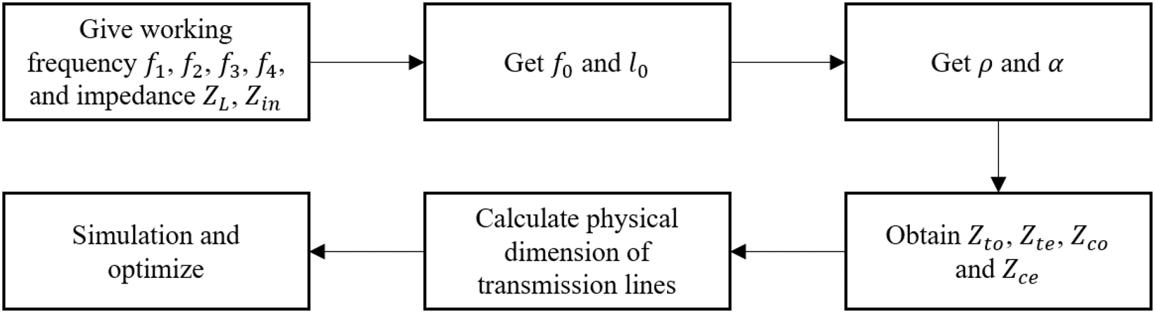
Design process is shown in Figure 2. If we give  ${f_1}$,
 ${f_2}$,
 ${f_3}$ and
 ${f_4}$ firstly,
 ${f_0}$ and
 ${l_0}$ can be calculated by (21) and (22). Second,
 $\rho $ and
 $\alpha $ can be calculated by (24) and (25). Third, we can know the image impedance
 ${Z_t}$ and
 ${Z_c}$ from (12). Then, according to (1), (2) and (3), the odd and even mode characteristic impedance
 ${Z_{to}}$,
 ${Z_{te}}$,
 ${Z_{co}}$, and
 ${Z_{ce}}$ can be obtained. Eventually, the basic parameters of the Quad-band impedance transformer can be determined.
Design process.

Type II: coupled line shunted at the source
As type II shown in Figure 1(b), with the stubbed coupled line section shunted at the source, the equations can be derived similarly. According to the transmission line theory, we can also give the input Impedance  ${Z_{in}}$ of two-section line.
 \begin{equation}\begin{array}{*{20}{c}}
{{Z_{in}} = \frac{{\frac{{{Z_c}}}{{j\tan {\varphi _c}}}{Z_L}^{{\text{''}}}}}{{\frac{{{Z_c}}}{{j\tan {\varphi _c}}} + {Z_L}^{{\text{''}}}}}}
\end{array}\end{equation}
 \begin{equation}\begin{array}{*{20}{c}}
{{Z_L}^{{\text{''}}} = {Z_t}\frac{{{Z_L} + j{Z_t}\tan {\varphi _t}}}{{{Z_t} + j{Z_L}\tan {\varphi _t}}}}
\end{array}\end{equation}
Similarly, the solutions are obtained by solving the equations as follows:
 \begin{equation}\begin{array}{*{20}{c}}
{\left\{ {\begin{array}{*{20}{c}}
{{Z_t} = \sqrt {{Z_{in}}{Z_L} - \frac{{{Z_L}\left( {{Z_L} - {Z_{in}}} \right)}}{\alpha }} } \\
{{Z_c} = \frac{{\alpha {Z_t}{Z_{in}}}}{{{Z_{in}} - {Z_L}}}}
\end{array}} \right.}
\end{array}\end{equation}
These two structures mirror each other, and the design process is the same as described in the case that the stubbed coupled line section C is shunted at the load end. To match real impedance load, it can be seen that in (12) that  ${Z_0}$ should be smaller than
 ${Z_L}$, however in (28),
 ${Z_0}$ should be larger than
 ${Z_L}$, which means that cases change with structures changing.
Analysis and simulations
The solutions mentioned above are elementary in nature and are in open-circuit form. However, not all frequencies are ideal for realizing the application, so we must consider the available ranges of frequency ratios. Thus, to describe the relationship between different frequencies better, we let  ${f_2} = p{f_1}$,
 ${f_3} = q{f_2}$,so
 ${f_3} = pq{f_1}$, where
 $p$,
 $q$ is the frequency-ratio and
 $1 \lt p \lt pq$. So we can rewrite (24) as follows by replacing frequencies.
 \begin{equation}\begin{array}{*{20}{c}}
{\rho = \tan \frac{\pi }{{p\left( {q + 1} \right)}}\tan \frac{{p\pi }}{{p\left( {q + 1} \right)}}}
\end{array}\end{equation}
Then, we obtain by (29) since  $\rho \gt 1$.
 \begin{equation}\begin{array}{*{20}{c}}
{\frac{{\sin \frac{\pi }{{p\left( {q + 1} \right)}}\sin \frac{{p\pi }}{{p\left( {q + 1} \right)}}}}{{\cos \frac{\pi }{{p\left( {q + 1} \right)}}\cos \frac{{p\pi }}{{p\left( {q + 1} \right)}}}} \gt 1}
\end{array}\end{equation}
We can get  $\cos \frac{\pi }{{p\left( {q + 1} \right)}} \gt 0$ and
 $\cos \frac{{p\pi }}{{p\left( {q + 1} \right)}} \gt 0$ since
 $1 \lt p \lt pq$. Equation (30) can be derived as follows after rearrangement and using trigonometric formula.
 \begin{equation}\begin{array}{*{20}{c}}
{\cos \frac{{\left( {p + 1} \right)\pi }}{{p\left( {q + 1} \right)}} \lt 0}
\end{array}\end{equation}
The solution of Equation (31) is
 \begin{equation}\begin{array}{*{20}{c}}
{\frac{{2 - p\left( {4n + 1} \right)}}{{p\left( {4n + 3} \right)}} \lt q \lt \frac{{2 + p\left( {1 - 4n} \right)}}{{p\left( {4n + 1} \right)}}}
\end{array}\end{equation}
Where  $n$ is an arbitrary integer. With
 $1 \lt p \lt pq$, (32) can be simplified as
 \begin{equation}\begin{array}{*{20}{c}}
{1 \lt q \lt \frac{{2 + p}}{p}}
\end{array}\end{equation}
Multiply by  $p{f_1}$, we obtain
 \begin{equation}\begin{array}{*{20}{c}}
{{f_1} \lt {f_2} \lt {f_3} \lt 2{f_1} + {f_2}}
\end{array}\end{equation}
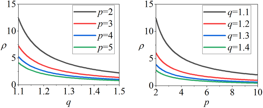
Figure 3 shows the relationships between the impedance ratio  $\rho $ and frequency ratio
 $p$ and
 $q$, we can obtain this conclusion that ratio
 $\rho $ is reducing with the increase of
 $p$ and
 $q$, which means ratio
 $\rho $ is reducing with the increase of designed frequency ratio.
Relationship between  $\rho $, frequency-ratios
 $p$ and
 $q$.

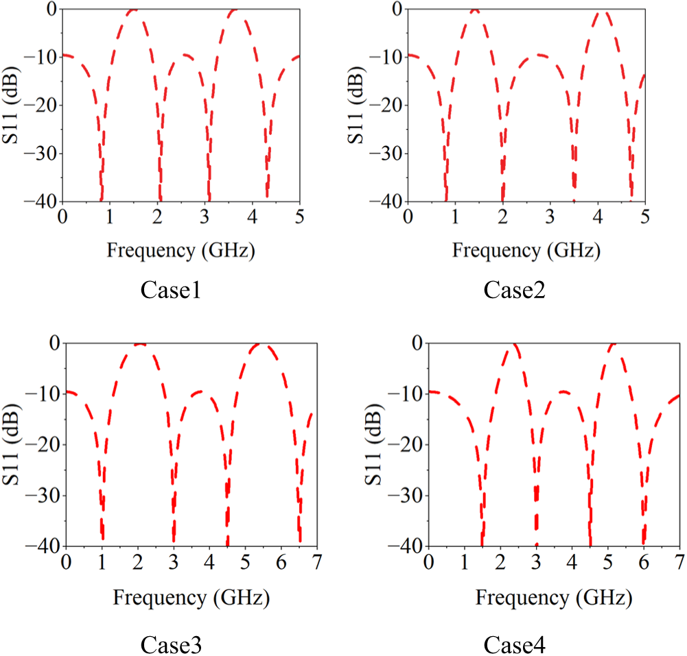
We give some examples under the condition that  $K = 0.5$, as listed in Table 1. Figure 4 shows the theoretic
 $\left| {{S_{11}}} \right|$ under the condition with fixed
 ${f_1}$,
 ${f_2}$ and
 $p = 2.5$ and fixed
 ${f_2}$,
 ${f_3}$ and
 $q = 1.5$. It can be seen that the
 $\left| {{S_{11}}} \right|$ is well-matched with designed frequencies.
Theoretic  $\left| {{S_{11}}} \right|$ under the conditions from Table 1.

Simulations on condition  $K = 0.5$ (
 $p = 2.5$ or
 $q = 1.5$)

Experiment results
Considering non-TEM behavior in microstrip realization in the application, a stepped impedance coupled line is used in model building [Reference Schiek and Kohler19].To verify the matching at the four frequency points, we choose F4BM-2 ( $tan{ }\delta \leqslant 0.0007$) with a relative permittivity of 2.55 and the thickness
 $h$ of
 $0.762mm$ as the dielectric substrate to fabricate a quad-band impedance transformer at 0.7/2.4/3.6/5.3 GHz, which could be applied to Power Divider, Coupler, Antenna, Filter, Mixer Power Amplifier, and LNA. Here we set
 ${Z_0} = 50{\Omega }$ and
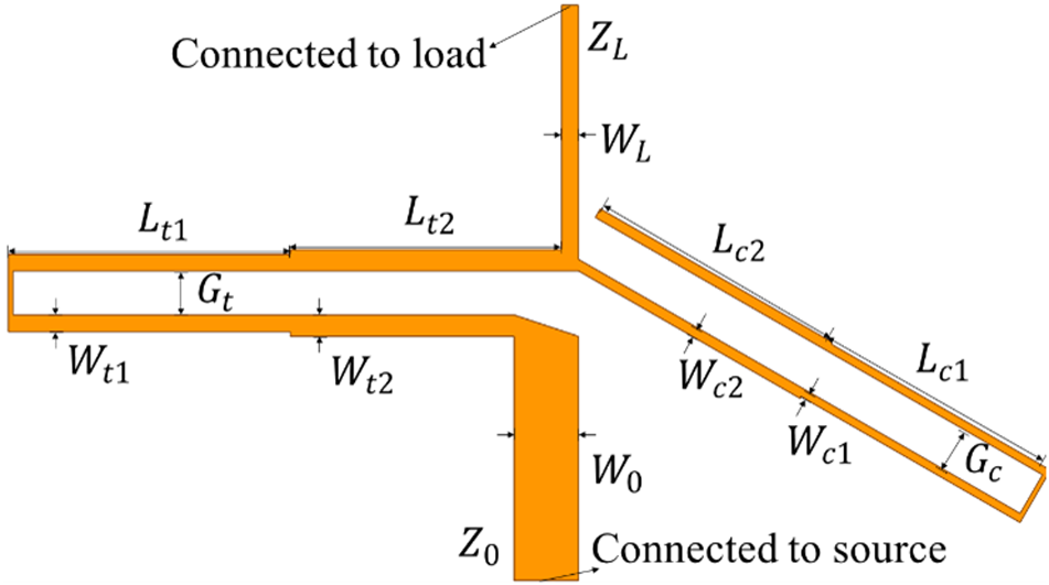
 ${Z_L} = 100{\Omega }$. The model of the designed impedance transformer with the dimension being labeled and the photo of it are shown in Figure 5 and Figure 6. The numerical results are calculated by MATLAB R2022b, and we obtain the simulated results by Advanced Design Systems (ADS).
The model of the designed impedance transformer with the dimension being labeled.

The photo of the designed impedance transformer.

By the equations above, we can calculate that  ${Z_{te}} = 102.19{\Omega }$,
 ${Z_{to}} = 86.50{\Omega }$,
 ${Z_{ce}} = 133.09{\Omega }$,
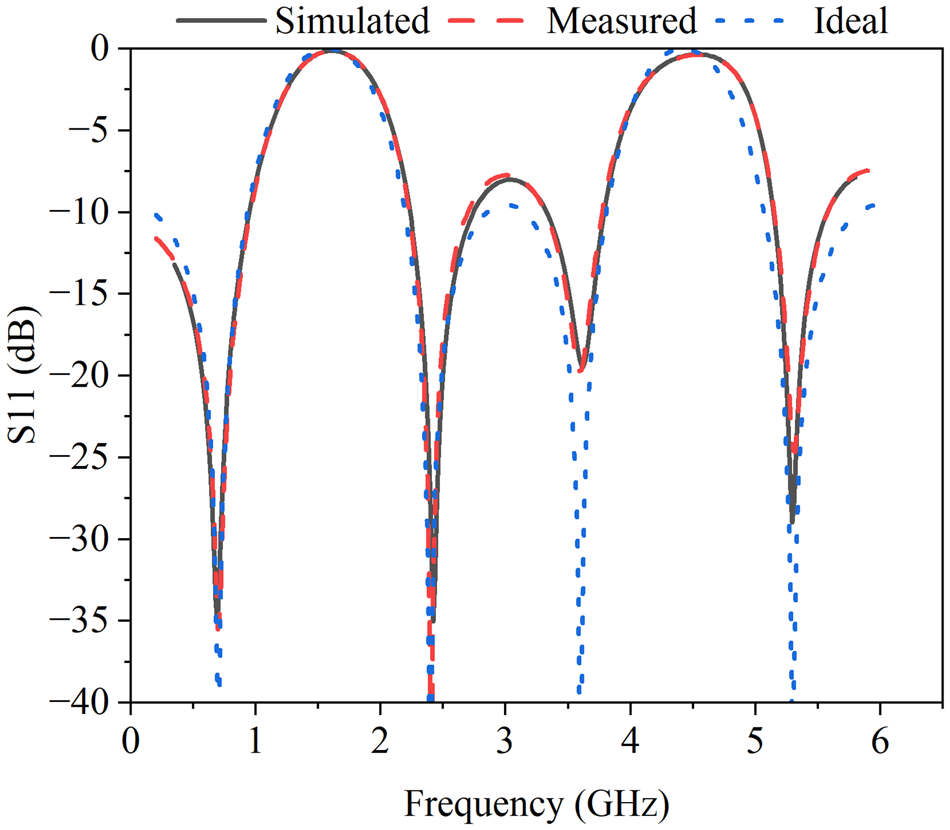
 ${Z_{co}} = 112.66{\Omega }$. Then, we optimize the result through simulation and final dimensions are listed in Table 2. It is shown in Figure 7 about the measured results of S-parameters for the magnitude of
 $\left| {{S_{11}}} \right|$ obtained from the Agilent N5230A network analyzer and the simulated results. We can directly see that the measured results of the
 $\left| {{S_{11}}} \right|$ are about −35.5 dB at 0.7 GHz, −35.8 dB at 2.4 GHz, −19.7 dB at 3.6 GHz, and −24.5 dB at 5.3 GHz. The two curves fit very well in Figure 7, which means that the measured results are in good agreement with the simulated results at four designed frequencies. The designed impedance is practicable. Compared with the result in Chongcheawchamnan et al. [Reference Wang, Zhang, Xu, Bai, Liu and Shi17], simulated and measured curves fit better in this paper. There are some small differences between measured and simulated results, these could be caused by material purity, manufacturing limitation, coaxial line connector welding, and measurement accuracy.
Simulated and measured  $\left| {{S_{11}}} \right|$ results of the designed impedance transformer.

Optimized dimensions (unit millimeter)

Conclusion
In this paper, we propose a novel quad-band impedance transformer. The proposed impedance transformer can match a real impedance load at four frequencies by using a stubbed coupled line and reduce the impedance transformer’s size. Firstly, we give and analyze two types of structures of the proposed impedance transformer and derive design equations logically, which validates the feasibility of the design theoretically. Then, considering the available ranges of frequency ratios, we derive them numerically and several cases are listed and evaluated to prove the feasibility of the application of the designed impedance transformer. The costs of manufacture could be reduced by reducing the grounding holes. Finally, a quad-band transformer working at 0.7/2.4/3.6/5.3 GHz is manufactured and measured to verify the consistency between simulation and application. Considering non-TEM behavior in microstrip realization in the application, a stepped impedance coupled line is used in model building to overcome it. It turns out that the measured results are in good agreement with the simulated results.
Acknowledgement
This work was supported by the Key Research and Development Program of Shaanxi Province under Grant 2020ZDXM5-01.
Competing interests
The authors report no conflict of interest.

Xinhuai Wang received the B.E. degree in electronic science and technology and Ph.D. degree in radio physics from Xidian University, Xi’an, China, in 2004 and 2010, respectively. Since 2010, he has been with the National Key Laboratory of Antennas and Microwave Technology, Xidian University, as a Lecturer. He has been an Associate Professor with Xidian University since 2014. He is currently a Professor and Doctoral Supervisor since 2020. His recent research interests are mainly in microwave circuits and smart antenna system design.

Kejiang Li was born in Chengdu, Sichuan, CHN in 1998. He received the B.E. degree in electronic information engineering from Xidian University, Xi’an, China, in 2022. He is pursuing a master’s degree in electronic and information from Xidian University. His recent research interests include flexible antenna, millimeter wave radar, and impedance transformer.

Yifan Hou was born in Hanzhong, Shaanxi, CHN in 2000. He received the B.E degree in electronic engineering from Xidian University, Xi’an, China, in 2022. He is pursuing a master’s degree in electronic and information from Xidian University. His recent research interests include RF circuits and systems, microwave device simulation and design, as well as smart antenna design.

Wen Wang was born in Xi’an, Shaanxi, CHN in 1998. He received the B.E degree from Northwestern Polytechnical University, Xi’an, China.in 2018, and the M.E degree from Nanjing Research Institute of Electronics Technology, Nanjing, China, in 2021. He is currently pursuing thePh.D. degree in electronic science and technology from Xidian University, Xian, China. His current research interests include wearable, antenna, and radio frequency technologies and applications.

Hongyang Xu was born in Jining, Shandong, CHN in 1997. He received the B.E. degree from Qingdao Agricultural University, Qingdao, China in 2020, and the M.E. degree in New Generation Electronic Information Technology from Xidian University, Xi’an, China in 2023. His current research includes microwave and radio frequency (RF) technology, millimeter wave radar signal processing, and embedded systems development.

Yin Xu received the B.E., M.E., and Ph.D. degrees from Xidian University, Xi’an, China, in 2006, 2009, and 2013, respectively. She is working at Xidian University as an Associate Professor. Her recent research interests are mainly in the electromagnetic field and microwave technology.

Xiaowei Shi received the B.E., and Ph.D. degrees from Xidian University, Xi’an, China, in 1982 and 1995, respectively. He is engaged in teaching and research in the field of electromagnetic field and microwave technology at the School of Electronic Engineering, Xidian University. His recent research interests include: computational electromagnetics, array antennas, smart antennas, radio frequency identification, and microwave circuits and systems.