I. INTRODUCTION
Transmission electron microscopy (TEM) with in situ ion irradiation can give invaluable insights into the response of materials to radiation. Traditional ex situ studies are inevitably limited to the study of end states and thus are unable to capture the dynamic evolution of microstructures. Although multiple irradiation steps can be performed with transfer to another instrument for characterization after each step, this process can be time consuming and the number of steps limited by the fragility and/or contamination of the sample. Furthermore, it can be problematic to maintain the same experimental conditions such as temperature throughout irradiation, transfer, and observation. In the case of a TEM sample, it can be difficult to return to exactly the same nanosized region especially given the morphological changes which can occur under irradiation. However, TEM with in situ ion irradiation can overcome these challenges by constantly following the same region of a sample from virgin to end-fluence whilst controlling variables such as temperature and minimizing the risks incurred during sample transfer.
In 1961, the creation of black-spot damage in gold samples under TEM observation was reported by Pashley and Presland Reference Pashley and Presland1 working at the Tube Investment Laboratories, Cambridge (UK). They suspected that these could “arise from bombardment by energetic negative ions emitted from the tungsten filament of the electron gun”. Reference Pashley and Presland1 To rule out electron beam effects, they used deflection coils mounted above the sample position in their Siemens Elmiskop I 100 kV TEM as a mass-selector to deflect the electrons away from the sample whilst not causing significant deviation of any ions. After an hour with the electron beam and coils turned on, a previously virgin sample was found to contain the same black-spot damage despite the electron beam having been deflected away by the coils. In another test, two gold samples were loaded above and below each other such that ions would be stopped in the top foil but with electrons able to pass through both foils. The objective lens could be used to form a TEM image of either the top or bottom sample. The radiation damage was observed in the top sample with very little in the bottom sample. Pashley and Presland concluded that the “direct observation of ion damage in the electron microscope thus represents a powerful means of studying radiation damage” Reference Pashley and Presland1 and the technique of TEM with in situ ion irradiation was born.
The story now moves to Canada and the Chalk River Nuclear Laboratories in the mid-1960s. Howe et al. Reference Howe, Gilbert and Piercy2–Reference Howe, McGurn and Gilbert5 used another Siemens Elmiskop I with an electron filament coated so as to enhance the flux of O− ions. Their experiments on radiation damage in copper, gold, and aluminum below 30 K were also the first experiments to combine low temperature and ion irradiation with in situ TEM. In another first, a Faraday cup was installed to allow measurement of the ion beam flux within the microscope column. Reference Parsons and Howe4
Later in the same decade came the first TEM to be interfaced with an external ion-accelerator in the laboratories of the Atomic Energy Research Establishment at Harwell (UK). Reference Thackery, Nelson and Sansom6,Reference Thackery and Nelson7 This instrument consisted of a JEOL JEM-6A connected to a 120 kV heavy-ion accelerator and featured electrostatic deflection on the outside of the TEM column to achieve an angle of 35° between the electron and ion beams. This facility was later upgraded to a JEOL JEM-200A in the early 1970s. Reference Whitmell, Kennedy, Mazey and Nelson8
Further systems were developed throughout the 1970s, including at the University of Virginia (USA), Reference Jesser, Horton and Scribner9 the Centre de Sciences Nucléaires et de Sciences de la Matière (CSNSM) Orsay (France), Reference Ruault, Lerme, Jouffrey and Chaumont10 and the University of Tokyo (Japan). Reference Ishino, Kawanishi and Fukuya11 In the 1980s and 1990s, there followed several facilities such as: the High Voltage Electron Microscope (HVEM) Reference Taylor12,Reference Taylor, Wallace, Ryan, Philippides and Wrobel13 and Intermediate Voltage Electron Microscope (IVEM) Reference Allen, Funk and Ryan14 both at Argonne National Laboratory (USA); the JEOL JEM-ARM1000 at the National Institute for Materials Science (NIMS) Reference Furuya, Piao, Ishikawa and Saito15 and JEOL JEM-ARM1300 at Hokkaido University Reference Hinks16 (both Japan); and more recently, the Joint Accelerators for Nano-science and Nuclear Simulation (JANNuS) facility at CSNSM Orsay (France), Reference Serruys, Ruault, Trocellier, Henry, Kaïtasov and Trouslard17 the Microscope and Ion Accelerator for Materials Investigations (MIAMI) facility at the University of Huddersfield (UK), Reference Hinks, van den Berg and Donnelly18 and the In situ Ion Irradiation TEM (I3TEM) facility at the Ion Beam Laboratory at Sandia National Laboratories (USA). Reference Hattar, Bufford and Buller19 The interested reader is directed to previous reviews on the technique of TEM with in situ ion irradiation. Reference Hinks16,Reference Ishino20–Reference Serruys, Ruault, Trocellier, Miro, Barbu, Boulanger, Kaïtasov, Henry, Leseigneur, Trouslard, Pellegrino and Vaubaillon26
A. Ion beam selection
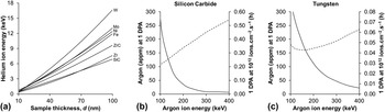
The choice of ion species and energy for an in situ TEM experiment needs to be made with attention paid to sample thickness, orientation, and composition as well as the phenomena to be investigated. Figure 1(a) shows the results of “detailed calculations with full damage cascades” performed using the Stopping Range of Ions in Matter (version SRIM-2013.00) Monte Carlo computer program Reference Ziegler, Ziegler and Biersack27 for helium irradiation of a selection of nuclear materials at normal incidence for a range of typical TEM sample thicknesses, d, from 10 to 100 nm. To achieve a projected range, R p, in the middle of a sample (i.e., R p = 0.5 d) to study, for example, helium accumulation in these materials requires just 3.3 keV for a 50 nm sample of silicon carbide but 16.8 keV for 100 nm of tungsten.
Results of SRIM Reference Ziegler, Ziegler and Biersack27 calculations for: (a) the helium ion energy required to achieve a projected range in the middle of a sample of various nuclear materials; and the amount of implanted argon (solid lines) and irradiation time (dashed lines) for 1 DPA with a flux of 1012 ions cm−2 s−1 in a 50 nm sample of (b) silicon carbide and (c) tungsten illustrating how higher energies can be used to minimize implantation in a TEM sample when investigating the effects of atomic displacements but at the cost of increased irradiation times. Note the order of magnitude difference in the irradiation times between (b) and (c).

Where the purpose of the experiment is to explore the accumulation of atomic displacements (measured in Displacements Per Atom (DPA)), then heavy inert gas ions or self-ions can be used. (At 1 DPA, every atom in the target has, on average, been displaced once from its lattice site.) However, when irradiating to high levels of DPA, the amount of implanted gas or additional interstitial atoms should be considered as these can become significant factors. Figures 1(b) and 1(c) show the Atomic Parts Per Million (APPM) per DPA averaged over a 50 nm target in the cases of silicon carbide (low Z) and tungsten (high Z) for a range of argon ion energies. As can be seen, the amount of implanted gas can be minimized by using higher energy ions which are more likely to travel all the way through a thin TEM sample. However, this can result in a lower number of atomic displacements as the exiting ion retains a proportion of its incident energy (rather than depositing it in the target) and the collision cross-sections of the target atoms decrease with increasing ion energy. Therefore, whilst it is possible to use higher energies to reduce the degree of ion implantation, a trade-off must be made with respect to the irradiation time required to achieve a given DPA level as shown in Figs. 1(b) and 1(c) for the example of the time to reach 1 DPA with a typical ion flux of 1012 ions cm−2 s−1.
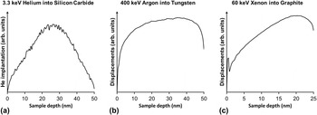
Another consideration, beyond the total number of implanted ions or atomic displacements, is the distribution of the ions and/or damage within the TEM sample. Selection of the appropriate ion energy can be used to put helium in the middle of the foil as shown in Fig. 2(a) for 3.3 keV helium implantation into silicon carbide or to achieve a relatively uniform distribution of damage across the sample thickness as shown in Fig. 2(b) for 400 keV argon irradiation of tungsten. This approach helps to ensure that the maximum helium is retained in the sample and that observations are made at the intended DPA levels, respectively. Failure to design an experiment appropriately could, for example, lead to excessive loss of an implanted species at a surface or give results distorted by a peak DPA level in a nonuniform damage profile. Alternatively, it may be desirable to deliberately skew a distribution within the sample. For example, graphitic materials are known to exhibit basal plane contraction under displacing irradiation with the degree of dimensional change being a function of the number of atomic displacements. Reference Perks and Simmons28,Reference Henson, Perks and Simmons29 By using 60 keV xenon ions to create an asymmetric damage profile similar to that shown in Fig. 2(c), it has recently been demonstrated that it is possible to induce significant strain within a sample due to the differential rates of basal plane contraction. Reference Hinks, Haigh, Greaves, Sweeney, Pan, Young and Donnelly30
Results of SRIM calculations showing: (a) a peaked implantation profile for 3.3 keV helium irradiation of silicon carbide; (b) a damage profile which is relatively flat over most of the sample depth for 400 keV argon irradiation of tungsten; and (c) a skewed damage profile for 60 keV xenon irradiation of graphite.

As well as species and energy, the ion beam flux is of course also a critical parameter. For many experiments, the main considerations will be the required end-fluence and timescale for the irradiation. However, some experiments such as those into rate effects or single-ion phenomena may be very prescriptive as to the flux required. To take the latter example, to have events happen neither too often nor too infrequently, it may be desirable to have a single ion arrive on average every 10 s in a 100 × 100 nm area requiring a flux of 109 ions cm−2 s−1 or in a 1 µm long-section of 50 nm diameter nanowire irradiated normal to its axis requiring 2 × 10⁸ ions cm−2 s−1.
Rather than selecting the species and energy to control the number of implanted ions or displaced atoms and/or their distributions, another approach to experimental design is to aim to create primary knock-on atoms (PKAs) within a particular energy range so that they are, for example, below an energy threshold required to cause atomic displacement or comparable to those created by neutrons.
B. Simulation of neutron irradiation
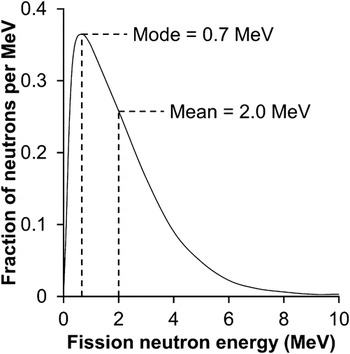
Once a PKA of a given energy has been created by an atomic displacement event, the subsequent processes such as the atomic collision cascade, thermal spike phase, and resulting point defect behavior are determined only by the physical properties of the sample which is under irradiation. It does not matter whether the PKA was displaced by an electron, proton, neutron or ion. In this sense, ion beams can be used to simulate neutron irradiation directly. A typical fission neutron energy spectrum peaks at around 0.7 MeV as shown in Fig. 3. At that energy, the maximum energy which can be transferred to, for example, an iron atom is about 48 keV assuming a purely elastic binary collision. That is the same maximum energy transferable to an iron atom by a 48 keV Fe or a 50 keV Ar ion and so these, or similar, ion species and energies can be used to produce PKAs of comparable energies to those created by neutrons in a nuclear fission reactor.
Energy spectrum of the prompt neutrons created by thermal fission of uranium-235.

However, there are important differences between ion and neutron irradiation which should be acknowledged. Ion beams do not recreate a fission neutron energy spectrum (and therefore recoil energy spectrum) as shown in Fig. 3 and can also be limited as regards the maximum energy which can be transferred to a PKA given the long high-energy tail of the neutron energy spectrum up to around 15 MeV. The fundamental stopping mechanisms are also different because of role of electronic energy loss processes in addition to nuclear stopping in the ion case. An ion which in theory has sufficient energy to create a PKA comparable to the neutron case when it enters the sample will inevitably have lost some of its energy by the time it experiences its first significant atomic collision. The ion beams normally used in TEM with in situ ion irradiation do not induce nuclear transmutation events and thus phenomena such as the introduction of fission gas products are not replicated directly.
There are several major advantages of using ion beams to simulate neutrons as compared to direct neutron irradiation. As mentioned above, the ion beams typically used in TEM with in situ ion irradiation do not cause nuclear transmutation events and so do not induce radioactivity in the materials under irradiation. This has clear benefits in terms of safety precautions, sample handling, and instrument contamination. In addition, using heavy-inert or self-ion irradiation, in just a few hours, it is possible to reach DPA levels comparable to the end-of-life for nuclear reactor core components. The cores of some Generation IV reactor designs are expected to expose structural materials to up to 200 DPA. Reference Guérin, Was, Zinkle and Editors31 For example, using a 100 keV argon flux of 5 × 10¹² ions cm−2 s−1, it is possible to achieve 200 DPA in a 50 nm sample of iron in 3 h, of tungsten in 2 h or of silicon carbide in 8 h of irradiation.
Of course, achieving such high damage levels in a few hours compared to the decades it would take in a nuclear reactor under normal operating conditions raises issues regarding dose rate effects (the interested reader is directed to Chapter 11 of Ref. Reference Was32). This, along with other effects such as the proximity of surfaces in a thin TEM sample, must be taken into consideration when designing and interpreting experiments with a view to understanding irradiation in nuclear environments.
C. Angle between the ion and electron beams
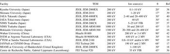
The angle, θ, between the ion and electron beams can be an important consideration in the design of in situ TEM facilities and experiments with smaller values of θ generally being more desirable. To reduce the chance of ion beam shadowing effects, it can be advantageous to bring the ion beam as close as possible to the electron beam to avoid shadowing of the ion beam by the internal surfaces of the microscope, the TEM-sample rod, and the support grid (if present) on which the sample is mounted. However, it is possible to successfully engineer around these challenges as demonstrated recently by both the JANNuS Reference Serruys, Ruault, Trocellier, Henry, Kaïtasov and Trouslard17 and I3TEM facilities. Reference Hattar, Bufford and Buller19
Sample sputtering is maximized when the ion beam makes an angle of about 30° to the surface at the point of incidence. Such effects may become significant at high fluences and in TEM foils are most easily observed as the loss of the thin edge regions. Sputtering yields can even be quantified if enough is known about the sample dimensions and geometry. Reference Greaves, Hinks, Busby, Mellors, Ilinov, Kuronen, Nordlund and Donnelly33 Even in facilities with large values of θ, this can be ameliorated by tilting the sample toward the ion beam. An additional benefit of this is to increase the projected range of the ions into the sample which can be an advantage in situations where the maximum ion energy available is a limiting factor. However, such sample tilting can increase the effective thickness of the sample in the direction of the electron beam and thus reduce the amount of usable electron-transparent area. A requirement to tilt toward the ion beam for the aforementioned reasons can unfortunately be restricting in terms of the crystallographic orientations which are available for achieving specific electron-diffraction conditions and in terms of the sample rod geometries which can be used without blocking the electron beam. Especially, for low-energy light-ion irradiation such as, for example, < 10 keV hydrogen or helium, an additional problem of large values of θ can be that the ions must traverse the strong magnetic field of the objective lens, B, at angles which result in the Lorentz force deflecting them away from the sample; although with appropriate ion beam alignment, this effect may be correctable so long as large changes of objective focus (and hence changes in B) are not required during the in situ irradiation experiment.
However, there are some potential benefits to large values of θ even up to 90°. Firstly, the connection of the ion accelerator to the TEM can be greatly simplified by introducing the ion beam via a side port on the microscope and then through the objective pole-gap to the sample position. Due to the construction of the lower-condenser and upper-objective sections of many TEMs, it can be difficult to bring in an ion beam over the top of the objective lens without expensive and complicated modifications to the upper objective pole-piece. Secondly, there are materials systems and experiments for which irradiation normal to the electron beam is not necessarily problematic or may even be desirable. For example, the surface of nanospheres and many other nanostructures do not form a single angle with the incident ion beam thus reducing the requirement to control sputtering through sample tilting and offering the possibility of observing the effects of irradiation on the incident and exit surfaces separately.
D. TEM sample design and preparation
TEM sample preparation must always be performed carefully with attention paid to the nature of the experimental work for which the samples are intended. However, in situ TEM techniques, and in particular the combination with ion irradiation, introduce additional factors which must be considered.
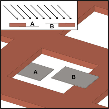
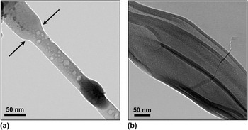
For samples requiring a support grid it is essential that the grid used does not block the ion beam as illustrated in Fig. 4. That said, it can sometimes be desirable to have some shadowing to preserve areas of a sample in the virgin state allowing direct comparison to the irradiated material after the experiment. A clear demonstration of this is shown in Fig. 5(a) where shadowing of a silicon nanowire by its support grid has preserved a section of the nanowire and enabled a necking structure to be engineered via ion beam sputtering of the exposed material. However, if the sample requires a mesh grid and such shadowing effects are not being sought, then as large as possible mesh hole size should be used to minimize the sample area which could potentially be shadowed from the ion beam. If a choice of grid thickness is available then thinner is better so long as this does not compromise the structural integrity of the sample and grid during the in situ experiment. Shadowing by the grid can often be avoided by ensuring that the sample is situated on the side of the grid on which the ion beam is incident. However, in some situations, this is not possible (for example when using oyster grids which enclose the sample in a mesh on both sides) and so the selection of mesh size and suitable sample orientation within the TEM become essential.
Schematic illustrating some geometric considerations when orientating a grid in the TEM with the ion beam incident in the direction indicated in the inset. Two samples are shown mounted on a typical mesh grid with A prone to shadowing and sputtering from the grid and with B more-suitably orientated.

TEM micrographs demonstrating the effects of: (a) shadowing of a silicon nanowire under 6 keV helium irradiation at 500 °C with boundary of shadowed region indicated by arrows and (b) curling of a thin region in a silicon carbide under 3.5 keV helium irradiation at 700 °C.

When commencing an experiment, the next step to avoiding shadowing is to select appropriate area(s) of the sample to observe. Typically, these will be regions a suitable distance from any part of the grid which could shadow the sample from the ion beam. It may also be necessary to select areas which are not only free from ion beam shadowing effects but also beyond the range of ion-beam-induced sputtering from the grid or other surfaces. These geometric considerations are illustrated in Fig. 4. Finally, it should also be noted that it is not just the ion beam which can be blocked. When approaching high degrees of sample tilt to avoid ion beam shadowing effects or to establish a specific orientation for the purposes of TEM characterization, the electron beam also has the potential to become shadowed. In these situations, mesh size, grid thickness, sample loading, and area-of-interest selection are all important factors with a good understanding of the experimental geometry and construction of the TEM being essential.
Similar considerations apply to the preparation and mounting of focused ion beam (FIB) milled samples onto lift-out grids. To avoid sputtering from the grid onto the sample during the in situ ion irradiation, it is important to position the sample level with the grid surface on which the ion beam will be incident in TEM. Then when loading the sample, the grid should be orientated so that the sample faces the ion beam with the grid behind it in the direction of the incident ions—similar to the orientation of sample B in Fig. 4.
As well as the grid and TEM sample holder, ion beam shadowing effects can also be caused by the sample itself. For example, in the study of nanostructures such as nanowires dispersed on support films, it is important that the specific structures being followed are not shadowed by their neighbors. When depositing nanostructures suspended in a solution, this can be assisted by the use of a suitably dilute mixture to reduce the areal density of the nanostructures on the grid. Other examples where self-shadowing can be problematic include crushed powders sprinkled directly on to support films or heavily wedged samples such as those prepared by the small angle cleavage technique (SACT) Reference McCaffrey34,Reference McCaffrey35 if not properly orientated with respect to the ion beam.
For in situ TEM experiments involving heating either intentionally through a heating holder (where heat is being supplied to the sample) or via the ion and/or electron beams themselves (where it may be necessary to remove heat from the sample), the thermal contact and conductivity between the sample, grid, and sample holder should be considered. In particular, support films such as carbon or Formvar do not necessarily offer adequate thermal conduction. The thermocouple of a TEM sample holder is normally connected to the furnace in which the sample is located so the temperature reading given by the control equipment is not necessarily the same as the temperature of a particular nanoscale region of the sample at the point of observation. The best approach to address this issue is inevitably application specific and careful thought should be given if precise knowledge of the temperature is required.
TEM samples with large electron-transparent regions are often ideal for traditional imaging and characterization. However, under in situ ion irradiation areas which are too thin may be prone to “curling” or “scrolling” resulting in the loss of not only those areas themselves but also areas which they obscure as they rotate as shown in Fig. 5(b). This can be a particular problem in samples produced using ion beam milling (IBM) preparation techniques which may feature extremely thin regions at the edges of samples. To mitigate the risk of sample curling in materials prone to this phenomenon, higher angles can be used for the final polishing stages of IBM to create a higher wedge angle featuring less of the thinnest material most likely to suffer this fate. The obvious cost of this approach is a reduced amount of electron transparent area available during the experiment. Once the sample is in TEM, the selection of region(s) to be followed during in situ ion irradiation should be made so as to avoid the proximity of material likely to respond to irradiation by curling.
Preparation techniques such as IBM and FIB which use ion irradiation to produce samples can of course introduce radiation damage themselves. For ex situ irradiation experiments, this can be a major issue as there can be ambiguity as to whether the radiation damage observed was caused exclusively by the irradiation conditions being studied and are not in some way related to the sample preparation technique. For in situ irradiation experiments, this can be less of an issue as the regions of interest can be characterized before, followed during and then characterized after irradiation. However, this does not means that pre-existing radiation damage is not an issue. For example, defects may be below the resolution limit of TEM or otherwise go undetected. The implantation of inert gases by IBM or gallium by FIB may not be immediately obvious but may influence the outcome of experiments. In situations where this is a concern, if possible it is advisable to perform additional experiments using alternative sample preparation techniques to confirm whether such effects are present.
E. Facilities around the world
There are currently 13 TEM with in situ ion irradiation facilities operating around the world as detailed in Table I. Since the publication of the last comprehensive review of such facilities in 2009, Reference Hinks16 two new facilities have been established at the Ion Beam Laboratory at Sandia National Laboratories (USA) Reference Hattar, Bufford and Buller19 and at the Centre de Recherche Public Gabriel Lippmann (Luxembourg).
TEMs with in situ ion irradiation operational in 2014.

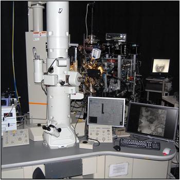
The I3TEM facility shown in Fig. 6 is located at Sandia National Laboratories (USA) and consists of a JEOL JEM-2100 coupled to a 6 MV tandem accelerator and a 10 kV Colutron ion source to provide a wide range of ion energies and species. Microfluidic and gas flow stages allow the in situ ion irradiation of systems such as metals undergoing corrosion opening up novel experimental possibilities not available previously in such facilities.
The recently established I3TEM at the Ion Beam Laboratory at Sandia National Laboratories (USA) Reference Hattar, Bufford and Buller19 (image courtesy of K. Hattar at SNL).

Another unique facility has recently been established at the Centre de Recherche Public Gabriel Lippmann (Luxembourg) and consists of an FEI Tecnai F20 fitted with a 35 kV gallium FIB. Reference Wirtza, Dowsetta, Vanhovea and Fleminga36 Although a TEM has previously been equipped with an in situ FIB at NIMS, Reference Tanaka, Furuya and Saito37 this new instrument is also equipped with a secondary ion mass spectrometer (SIMS) to analyze the atoms sputtered from precise regions using the FIB.
II. SUMMARY
TEM with in situ ion irradiation is ideally suited to study the dynamic processes of radiation damage. It makes possible the direct observation of the microstructure during bombardment whilst also allowing experimental variables such as temperature to be controlled and maintained. Through careful sample preparation and selection of ion species, energy, and flux, it is possible to tailor the experimental design to explore specific conditions and phenomena. The technique has been developing for over 50 years and there are currently 13 facilities in operation around the world. This is a field which will continue to grow to meet the challenges of developing new nuclear materials, of engineering nanostructures and of semiconductor processing as well as many other applications.