Introduction
Tools and their functionality often evolve through fusion of simpler instruments. Within the scope of nanotechnology, an evolution has resulted in the focused ion beam-scanning electron microscope (FIB-SEM) instrument. Gallium-based FIB systems, as we know them today, were developed in the 1980s and were quickly adopted by the semiconductor industry as a tool for analysis, repair of masks, and integrated circuit edit. Reference Melngailis, Musil, Stevens, Utlaut, Kellogg, Post, Geis and Mountain1,Reference Tao, Wilkinson and Melngailis2 In the 1990s, FIB and SEM columns were combined to form the two beam platform. Reference Gianuzzi and Stevie3 With further integration of a variety of detectors, a nano-manipulator and a temperature-controlled stage, FIB-SEMs became multifunctional tools that provide a myriad of unique characterization, fabrication, and sample preparation capabilities. Here, we review recent developments and applications of FIB-SEMs for in situ characterization and manipulation of material at the micro- and nanoscale.
In these applications, the sample may be mechanically or electrically excited, have material subtracted or added via ion milling or ion beam-induced deposition (IBID) or electron beam-induced deposition (EBID), Reference Utke, Hoffmann and Melngailis4 and have its temperature varied from above room temperature to cryogenic levels. Sample manipulation using nano-/microscale probes, which is often necessary to arrange the samples for their analysis or to construct a system, is a common theme across the reviewed FIB-SEM uses. Reference Gianuzzi and Stevie3 Mechanical, electrical, and/or thermal contacts between the nano-manipulators and the nano-/microscale objects of interest consist of localized welds made using EBID or IBID of carbon, metal, Reference Utke, Hoffmann and Melngailis4 electron-curable polymeric glues, 5 and, at cryogenic temperatures, ice deposition. Reference Antoniou, Graham, Hartfield and Amador6 Mechanical handling can also be achieved without any deposition through use of micro-grippers Reference Tuck, Ellis, Geisberger, Skidmore and Foster7 and, in some cases, just physical contact. Reference Antoniou8 This article describes the current state of the art of this experimental methodology, provides case studies in the areas of mechanical, electrical, and cryogenic characterization, and provides an outlook for new opportunities for in situ characterization and manipulation using FIB-SEMs.
Mechanical testing
Over the past decade, there has been tremendous growth in the use of two beam instruments to advance in situ mechanical test methodologies that operate on samples with micro- or nanometer scale dimensions. Characterization of the mechanical properties of a material at this scale is important because the deformation mechanisms are strongly affected by the sample dimensions. For this, FIB-SEMs are used in many aspects of the experiments, including preparation of the micromechanical test samples from bulk material, Reference Uchic, Dimiduk, Florando, Nix, Mills, Eggeler, George and Inui9–Reference Volkert and Minor11 transfer of the samples into the mechanical actuation device, Reference Gianola, Sedlmayr, Mönig, Volkert, Major, Cyrankowski, Asif, Warren and Kraft12 observing the sample deformation with the SEM, Reference Shade, Wheeler, Choi, Uchic, Dimiduk and Fraser13–Reference Kim and Greer15 characterization of local lattice rotation during the test, Reference Niederberger, Mook, Maeder and Michler16,Reference Kiener, Guruprasad, Keralavarma, Dehm and Benzerga17 preparation of TEM lamellae for dislocation substructure analysis, Reference Norfleet, Dimiduk, Polasik, Uchic and Mills18 and destructive 3D microstructural characterization after testing. Reference Shade, Groeber, Schuren and Uchic19
One of the most important applications for FIB-SEM technology is the localized preparation of micro- and nanoscale samples using a machining approach akin to those employed in abrasive water jet cutting. There has been significant growth in the use of this approach to manufacture miniature compression test samples in the last decade. Reference Uchic, Holzer, Inkson, Principe and Munroe20 The nearly universal milling ability of FIBs has resulted in the application of this micro-test sample fabrication methodology to a wide variety of materials, including pure metals, metallic alloys, metallic glasses, alkali halides, semiconductors, and biomaterials. Notably, utilizing advanced scripting capabilities to control both the ion beam and stage movement allows for complex machining strategies that provide for accurate control over the test sample geometry (creating samples with a uniform stress-state in the gage (active) region of the mechanical test sample) as well as automating the procedure for producing multiple samples. Reference Uchic and Dimiduk10,Reference Shade, Kim, Wheeler and Uchic21 Further advances are anticipated at the milli-to-mesoscale (i.e., characterizing samples that are many tens of micrometers or larger in dimension) with the advent of plasma FIB columns that can achieve orders of magnitude greater beam currents and material removal rates than the widely used gallium ion columns or through the use of other parallelized ion sputtering processes.
The recent maturation of in situ mechanical testing systems that operate within the two column systems has expanded the types of testing modes that can be accessed, notably tensile testing. Mechanical testing of other geometries, such as cantilever beam for bending Reference Motz, Weygand, Senger and Gumbsch14 and double shear, Reference Heyer, Brinckmann, Pfetzing-Micklich and Eggeler22 has also been demonstrated. The process of loading or attaching the sample to the test system grips is often non-trivial and can be greatly aided by live SEM imaging. In addition, for some experiments, the samples are freestanding such as in the case of nanowires, Reference Gianola, Sedlmayr, Mönig, Volkert, Major, Cyrankowski, Asif, Warren and Kraft12 and the two beam systems are used to transport samples into the test device. Manipulating small samples has not changed much in the past decade, and the state of the art remains the use of needle-tipped micromanipulators with EBID or IBID to “weld” the sample to the needle and eventually to the test frame. Using relatively large depositions, these structures are able to join the sample to test grips and provide a satisfactory hold while the sample is being loaded. Reference Gianola, Sedlmayr, Mönig, Volkert, Major, Cyrankowski, Asif, Warren and Kraft12 Improvements in non-adhesive-based methods such as micro-grippers and multi-axis manipulators should help simplify the process for assembling experiments in situ. Alternatively, samples can remain attached to a bulk substrate at one end, simplifying some of the micromanipulation challenges.
A variety of in situ mechanical testing systems are commercially available for use in FIB-SEMs, and similar technologies have been developed for TEMs. Smaller portable systems are directly mounted onto the FIB-SEM stage, while other systems are attached to the chamber. Initially, these test systems were used in conjunction with electron imaging to monitor the evolution of the sample during deformation. Current advancements have expanded the role of these systems for quantitative characterization of spatial heterogeneities associated with plastic flow using displacement image correlation methods Reference Gianola, Sedlmayr, Mönig, Volkert, Major, Cyrankowski, Asif, Warren and Kraft12,Reference Shade, Groeber, Schuren and Uchic19 and electron backscatter diffraction (EBSD) mapping. Reference Niederberger, Mook, Maeder and Michler16,Reference Kiener, Guruprasad, Keralavarma, Dehm and Benzerga17
One contemporary example of the use of two column instruments to enable in situ micromechanical testing can be found in the recent work of Shade et al., Reference Shade, Groeber, Schuren and Uchic19 who performed tension testing on pure Ni multicrystal samples. The objective of this study was to develop mechanical property data from samples that were comprised of about 200 grains in order to facilitate comparison to modern property simulation methods that utilize microstructural geometry and crystallographic orientation as an input. In this study, the capabilities of FIB-SEM systems were utilized in almost every step of the experiment.
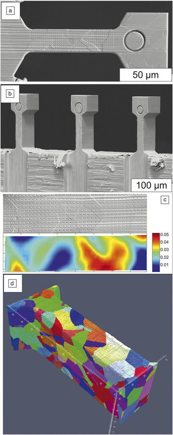
A composite image of the Shade et al. Reference Shade, Groeber, Schuren and Uchic19 study is shown in Figure 1 . Three mesoscale tensile samples were fabricated through coarse material removal using stencil masking and broad ion beam milling Reference Shade, Kim, Wheeler and Uchic21 followed by precise definition of the final sample dimensions using script-controlled automated FIB milling (see Figure 1a). In addition, low current FIB milling was used to define a submicrometer grid pattern of points on one surface of the sample to aid in local displacement mapping from one gage surface during testing.
Example of in situ mechanical characterization enabled by focused ion beam and scanning electron microscopes (FIB-SEMs). Reference Shade, Groeber, Schuren and Uchic19 (a–b) Tensile samples machined using a combination of broad ion beam and FIB methods. (c) SEM image and corresponding axial strain map calculated by displacement image correlation methods for a sample deformed to 2.5% axial strain. (d) 3D reconstruction of the grain structure from one of the tensile samples after in situ testing.

Subsequently, a custom micromechanical test frame Reference Shade, Wheeler, Choi, Uchic, Dimiduk and Fraser13,Reference Shade, Kim, Wheeler and Uchic21 was used to load the sample in tension, where the grip of the test frame was fabricated from a SiC fiber via FIB milling. Reference Wheeler, Shade and Uchic23 During the tests, high-resolution SEM images were collected throughout the loading cycle using a user-developed test control program that triggered secondary electron image collection at sequential levels of actuator displacement. These images were analyzed with custom software scripts to characterize the local surface strains throughout the test. A representative strain map for a sample experiencing ∼2.5% strain resulting from this analysis is shown in Figure 1c, and it highlights the local fluctuations in plastic flow for this multi-crystal sample. Note that while these specific in situ tensile experiments were performed in a single column SEM, similar experiments have been performed in two column instruments. In fact, the use of both columns can greatly aid the user when micro-manipulating the test sample into the testing system and may enable new approaches for 3D displacement mapping.
After the dynamic testing, the FIB-SEM was again employed to characterize the 3D grain structure of the sample by employing script-enabled serial sectioning and imaging experiments that included EBSD mapping at every section. This approach allowed the internal grain microstructure and local crystallographic orientation of the sample to be directly incorporated into crystal-plasticity finite element simulations. Reference Turner, Shade, Schuren and Groeber24 A 3D reconstruction of the sample described in the previous paragraph is shown in Figure 1d, and one can observe the high fidelity with which the grain structure from the entire gage volume can be quantified using FIB-SEM-based methods. From this brief example, one can envision new opportunities for in situ characterization of mechanical properties using the suite of capabilities provided by two beam systems.
Electrical testing and manipulation
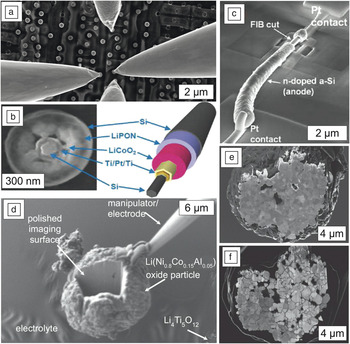
The FIB-SEM is used extensively in aiding nanoscale electrical characterization of integrated circuits as well as novel functional materials. The scaling down of integrated circuits, which makes access to and testing of individual components increasingly difficult, has been one of the primary industrial drivers for development and improvement of FIB-SEM technology. Reference Melngailis, Musil, Stevens, Utlaut, Kellogg, Post, Geis and Mountain1,Reference Tao, Wilkinson and Melngailis2 Within a two beam system, characterization and failure analysis can be performed even on an individual transistor. The transistor is isolated from its circuitry by using the FIB to first separate it from its surroundings and then to drill access vias into each node. Subsequently, landing pads for electrical probes are created by filling the via with a conductive metal using either EBID or IBID. Reference Song, Loh, Zheng, Neo and Oh25 While challenging in the past, all of the above steps can be currently performed in situ using a commercially available nanoprober with just a few electrical feed-through wires into the vacuum chamber (see Figure 2 a). Different failure sites of integrated circuits, whether “opens” or “shorts,” can also be revealed through selective electrical connections and excitation of the circuit imaged using voltage contrast SEM. Reference Goldstein, Newbury, Joy, Lyman, Echlin, Lifshin, Sawyer and Michael26,Reference Rosenkranz and Werner27
In situ electrical and electrochemical characterization and experiments. (a) In situ probing of a circuit using four electrodes. (b) A scanning electron microscope (SEM) image of a focused ion beam (FIB) cut cross-section and a schematic of a multishell nanowire core lithium ion battery (NWLIB). (c) SEM image of NWLIB on a Si/SiO2 substrate with the inner component locally exposed via FIB cutting and wired for electrical cycling with electron beam-induced deposition platinum electrodes. Reference Ruzmetov, Oleshko, Haney, Lezec, Karki, Baloch, Agrawal, Davydov, Krylyuk, Liu, Huang, Tanase, Cumings and Talin29 (b–c) Reprinted with permission from Reference 29. © 2011 American Chemical Society. (d) A microscale battery consisting of a single cathode oxide particle attached to a nanomanipulator probe that is used to immerse or partially immerse it into a liquid electrolyte droplet covering an anode material. (e–f) SEM images showing microstructure evolution of FIB-cut cathode material in setup shown in (d) prior to (e) and after three complete charge/discharge cycles. Reference Miller, Proff, Wen, Abraham and Bareño32 (d–f) Reprinted with permission from Reference 32. © 2013 Wiley.

Extensive research in the last two decades resulted in a bonanza of novel functional 1D, 2D, and 3D nanostructures such as nanotubes or nanowires, individual or stacked single atom sheets, and 3D nanoporous structures. These novel materials are often thought to have superior electrical properties, however, accurate measurements of these properties can be quite challenging due either to a complex architecture or large electrical contact resistance between the structure and the electrode material. Reference Leonard and Talin28 FIB-SEM provides a unique platform to test electrical properties of such materials. EBID and IBID are commonly used to reduce electrical contact resistance between nanotubes or nanowires aligned between two microfabricated electrodes or even to make the electrode patterns themselves. Reference Utke, Hoffmann and Melngailis4 Alternatively, conductive nanoprobes can be directly placed on the nanostructures to measure their electrical properties. This approach facilitates testing of nanostructures with non-planar geometries, for example vertically grown nanowires. The electrical contact resistance between the nanoprobe and the nanostructure is also reduced via EBID or IBID.
For electrical testing of complex multi-component nanomaterials, FIB-milling is also utilized for electrical test sample preparation. For example, Ruzmetov et al. Reference Ruzmetov, Oleshko, Haney, Lezec, Karki, Baloch, Agrawal, Davydov, Krylyuk, Liu, Huang, Tanase, Cumings and Talin29 recently used FIB milling to reveal, and EBID to wire, the inner components of a solid-state nanowire core-multishell Li-ion battery to prepare it for electrical cycling inside a high vacuum TEM (see Figure 2b–c). FIB-SEM is also used to integrate different nanostructures in-between two electron transparent membranes, often referred to as liquid cell, to enable in situ TEM imaging during electrical cycling in a liquid electrolyte. Reference Unocic, Adamczyk, Dudney, Alsem, Salmon and More30,Reference Gu, Parent, Mehdi, Unocic, McDowell, Sacci, Xu, Connell, Xu, Abellan, Chen, Zhang, Perea, Evans, Lauhon, Zhang, Liu, Browning, Cui, Arslan and Wang31 In turn, Miller et al. Reference Miller, Proff, Wen, Abraham and Bareño32 recently developed an alternative FIB-SEM-based method for imaging microstructure evolution of an Li-ion battery cathode material that was too thick to be imaged in the TEM. In particular, the authors imaged the microstructural evolution of a Li(Ni0.8 Co0.15Al0.05)O2-based cathode by attaching a microparticle of this material to the tip of a nanoprobe and dipping it in a low-vapor-pressure liquid electrolyte to connect it to the solid Li4Ti5O12 anode. Figure 2d–f shows that in order to reveal the microstructure, the inner parts of the cathode material were exposed via FIB milling. We expect that in the future, the FIB-SEM will continue to be used not only for sample preparation but also as a platform for novel in situ electrical and electrochemical studies, as exemplified by the work of Miller et al. Reference Miller, Proff, Wen, Abraham and Bareño32
Cryogenic FIB-SEM
While cryopreservation in combination with cryofracturing and cryo-ultramicrotomy have been used for decades to prepare samples for cryogenic electron microscopy Reference Echlin33,Reference Dubochet34 incorporation of a cryostage and cryo-vacuum transfer system onto a FIB-SEM is a much more recent advancement. Reference Heymann, Hayles, Gestmann, Giannuzzi, Lich and Subramaniam35–Reference Marko, Hsieh, Schalek, Frank and Mannella37 This approach is an alternative to room-temperature FIB-SEM characterization of porous and soft materials, which has been used to image polymers, Reference Bassim, De Gregorio, Kilcoyne, Scott, Chou, Wirick, Cody and Stroud38,Reference Bailey, Geurts, Stokes, de Jong and Barber39 geological, Reference Wirth40 and biological specimens. Reference Felts, Narayan, Estes, Shi, Trubey, Fu, Hartnell, Ruthel, Schneider and Nagashima41–Reference Bushby, P’ng, Young, Pinali, Knupp and Quantock44 Cryogenic processing avoids potential artifacts due to chemical fixation and heavy metal staining of cells, minimizes thermal damage induced by SEM imaging and FIB milling, Reference Bassim, De Gregorio, Kilcoyne, Scott, Chou, Wirick, Cody and Stroud38 and is also particularly attractive for imaging hydrated samples. Examples of cryo-FIB-SEM characterization of hydrated samples include imaging of unstained cells, Reference Heymann, Hayles, Gestmann, Giannuzzi, Lich and Subramaniam35,Reference Wang, Strunk, Zhao, Gray and Zhang45–Reference Edwards, Fay, Anderson, Scotchford, Grant and Brown50 determination of clay porosity at different moisture levels Reference Lubelli, de Winter, Post, van Hees and Drury51 and brine distribution in grain boundaries in halites, Reference Desbois, Urai, Burkhardt, Drury, Hayles and Humbel52 identification of a variety of nanomaterials in food Reference Dudkiewicz, Tiede, Loeschner, Jensen, Jensen, Wierzbicki, Boxall and Molhave53 and other consumer products, Reference Scott54 as well as drop, Reference Rykaczewski, Landin, Walker, Scott and Varanasi55 frost, Reference Rykaczewski, Anand, Subramanyam and Varanasi56 and ice Reference Subramanyam, Rykaczewski and Varanasi57 formation and adhesion mechanisms on nanoengineered superhydrophobic and lubricant-impregnated surfaces.
It was recently demonstrated that cryo-FIB-SEM can also be beneficial to the characterization of non-hydrated samples, for example, by reducing gallium poisoning of some inorganic materials such as compound semiconductors. Reference Antoniou, Graham, Hartfield and Amador6 The cryo-FIB-SEM processing procedure has been facilitated by improvements to the cryo-FIB milling procedure introduced by Hayles et al., Reference Hayles, Stokes, Phifer and Findlay58 who demonstrated that a protective organometallic coating can be deposited without the aid of ion or electron beams. In particular, this coating can be made by exposing the sample to a few-seconds pulse of the organometallic precursor gas, which rapidly freezes onto the cold surface. Subsequently, the ion beam is used to “cure” the frozen organometallic layer to increase its electrical conductivity.
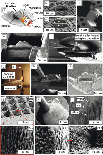
The improved quality of cryo-FIB milling and quantification of the Ga+ beam damage to the vitreous ice Reference Marko, Hsieh, Moberlychan, Mannella and Frank36,Reference Marko, Hsieh, Schalek, Frank and Mannella37 enabled two routes of using the cryo-FIB-SEM as an alternative to cryo-ultramicrotomy for preparation of high-quality samples for cryo-TEM. Reference Marko, Hsieh, Moberlychan, Mannella and Frank36,Reference Marko, Hsieh, Schalek, Frank and Mannella37,Reference Rigort, Bäuerlein, Villa, Eibauer, Laugks, Baumeister and Plitzko59–Reference Hayles, Matthijs de Winter, Schneijdenberg, Meeldijk, Luecken, Persoon, de Water, de Jong, Humbel and Verkleij61 In the first route, a frozen sample located either at a wedge-shaped end of a pre-trimmed tube Reference Hayles, Matthijs de Winter, Schneijdenberg, Meeldijk, Luecken, Persoon, de Water, de Jong, Humbel and Verkleij61 or on a TEM grid Reference Rigort, Bäuerlein, Villa, Eibauer, Laugks, Baumeister and Plitzko59 is FIB-milled to a thin film. Rigort et al. Reference Rigort, Bäuerlein, Villa, Eibauer, Laugks, Baumeister and Plitzko59 developed a clever variation of this technique, whereby a sample grown on a TEM grid is frozen and milled at an angle using cryo-FIB. After transfer under cryogenic and vacuum conditions, the resulting angled lamella can be tilted and imaged in the TEM (see Figure 3 a–e). The second route mimics room-temperature site-specific sample preparation but with an actively cooled lamella lift-out probe (Figure 3f–i). Reference Rubino, Akhtar, Melin, Searle, Spellward and Leifer60 In order to attach the sample to the lift-out probe and later to the lift-out TEM grid, a pulse and freezing of the organometallic gas or water vapor can be used. While cryo-lift-out is primarily intended for biological samples, Antoniou et al. Reference Antoniou, Graham, Hartfield and Amador6 demonstrated that it is also beneficial for anhydrous samples, such as GaAs and InN.
In situ manipulation and experimentation using a cryo-focused ion beam and scanning electron microscope (FIB-SEM): (a) cartoon, (b) before, and (c) after FIB view, and (d) top-down SEM view of TEM-lamella made using angled FIB-cut out of amoeba. (a–d) Reprinted with permission from Reference 59. © 2012 National Academy of Sciences of the United States of America. (e) Side-view of another angled lamella made using cryo-FIB; (f–i) cryo-lift-out system and procedure: (f) example of lamella attachment using ice rather than typical platinum deposition. (g) The tip of the nanomanipulator has been modified to be insulated (gray portion) from the rest of the assembly and thermally connected to the cooled anti-contaminator by Cu braids. (h) Extracted FIB-cut frozen lamella attached to the nanomanipulator tip using freezing of the platinium precursor gas. (i) Final lamella all prepared under cryogenic conditions after nanomanipulator removal and FIB-thinning. (f–i) Reprinted with permission from Reference 60. © 2012 Elsevier. (j–l) In situ directional frost growth on hierarchical superhydrophobic nano-pillar surface: (j) time sequence of SEM images at various magnifications showing nucleation and directional nano-icicle growth, (k) SEM image of the inserted water vapor GIS nozzle above the cooled substrate used to grow ice shown in (j), and (l) FIB-cut sections of the grown ice-nanostructure interface. Reference Rigort, Bäuerlein, Villa, Eibauer, Laugks, Baumeister and Plitzko59 (j–l) Reprinted with permission from Reference 63. © 2012 Cambridge. MTOC, microtubule-organizing center.

Applications of the cryo-FIB-SEM platform to nanofabrication and dynamic experiments are also emerging. Bresin et al. Reference Bresin, Toth and Dunn62 recently demonstrated that localized EBID of organometallic gas under cryogenic conditions not only increased the deposition speed by several orders of magnitude but also provided unique 3D nanostructure fabrication capabilities. In particular, selective electron beam-induced curing of the frozen organometallic layer combined with evaporation triggered via sample temperature increase can be used to make unique 3D structures with incorporated gaps. Reference Bresin, Toth and Dunn62 Rykaczewski and Scott Reference Rykaczewski and Scott63 used the cryo-FIB-SEM for in situ imaging of frost nucleation and growth on hierarchical superhydrophobic coatings. The unique advantages of performing this experiment in the cryo-FIB-SEM rather than in the typically used environmental SEM Reference Rubino, Akhtar, Melin, Searle, Spellward and Leifer60 are the capability of sample exposure to water vapor from various directions using a gas injection system, and imaging of ice-nanostructure interfaces revealed via FIB-milling at various frost growth stages (see Figure 3j–l). The previous examples illustrate the utility of cryo-FIB-SEM not only for cross-sectional and 3D imaging but also for cryo-lift-out and for in situ fabrication and experimentation.
Summary
Commercially available FIB-SEM instruments provide a unique combination of experimental capabilities—high resolution imaging, localized milling and deposition, and micro-manipulation—that when coupled with custom probe stations or stages, enable a suite of truly novel experimental methodologies. This article is focused on three common forms of external stimuli (mechanical, electrical, and temperature) that we consider to be most enabling, but note that there are other examples of innovative in situ FIB-SEM experiments that have not been covered. We anticipate that continued advances in the FIB-SEM platform such as novel ion beam sources, additional analytical detectors, and more precise actuation stages and micromanipulation technologies will enable further creative in situ measurements and experimentation. These developments will greatly aid the study of materials processes and properties at the nano- and microscale.
Acknowledgments
K.R. acknowledges funding from the Ira A. Fulton Schools of Engineering at Arizona State University. M.D.U. acknowledges support from the Materials & Manufacturing Directorate of the Air Force Research Laboratory. N.A. acknowledges funding from the Center for Nanoscale Systems (CNS), a member of the National Nanotechnology Infrastructure Network (NNIN), which is supported by the NSF (under Award No. ECS-0335765). CNS is part of Harvard University.