Introduction
When a low observable platform is designed, the antennas mounted over it are the major contributors of the overall radar cross section (RCS). Apart from shaping and using radar-absorbing materials and structures, antennas are made conformal to reduce the scattering effect. The RCS of low-profile antennas can further be reduced by an efficient design based on inclusion of defected ground plane, high impedance surface (HIS) elements, microwave absorber (MA), and superstrate [Reference Chen, Guo, Sang, Sun and Fu1–Reference Ramkumar, Chandrika and Rao5]. The main issue in design of low observable antennas is to achieve low RCS with desirable radiation performance parameters, viz., VSWR, antenna gain, angular coverage etc.
Initially, superstrates were used as a protective covering to low-profile antennas in severe environmental conditions. Then by using optimized design parameters of superstrate, the antenna performance was significantly improved, especially in terms of antenna gain and operating bandwidth [Reference Choi, Cho, Pyo and Choi6–Reference Zheng, Gao, Zhou, Cao, Yang, Li and Li9]. A superstrate essentially comprises of a dielectric layer of electromagnetic band gap (EBG) materials with frequency selective surface (FSS) elements or metasurfaces. It is placed at an optimum distance from the patch array toward maintaining desired antenna performance, but with low structural RCS. Furthermore, an FSS, single-substrate layer, broadband metamaterial absorber (MA) [Reference Sharma, Panwar and Khanna10–Reference Cheng, Ding, Peng, Feng and Liao12] can be included in the antenna array design to achieve low antenna RCS.
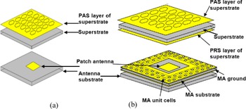
In this paper, a novel design of low RCS patch array with a HIS-based superstrate is presented. The superstrate layer consists of hexagonal-shaped unit cells, placed in a zig-zag pattern. This layer acts as a partially absorbing surface (PAS). Here, hexagonal element is selected in view of its advantage of having wider bandwidth [Reference Dorostkar, Islam and Azim13–Reference Meng, Li, Fan, Li, Xue, Chen and Wua15]. A rectangular-shaped slot element is introduced at the center of the unit cell in order to disturb the continuous surface current distribution, thereby improving scattering characteristics. These hexagonal aperture unit cells are arranged periodically on the superstrate. The configuration of superstrate consists of multilayered, viz., two-layered and three-layered structures (Fig. 1). In a two-layered structure, the antenna along with superstrate is designed where the superstrate composed of partially absorbing surface as upper layer. In three-layered structure, other than antenna and superstrate a metamaterial absorbing surface is introduced in the configuration. The superstrate comprised of partially absorbing surface (PAS) as upper layer and partially reflecting surface as lower layer (PRS). The PAS layer (upper) absorbs a part of incident out-of-band frequencies. The remaining out-of-band frequencies reaching PRS layer (lower) would get reflected. On the other hand, the in-band frequencies penetrate through the PRS layer and will be absorbed or diffracted in other directions by MA placed in the plane of patch antenna.
Schematic representation of superstrate configurations. (a) Two-layered structure: antenna with superstrate, (b) three-layered structure: antenna with superstrate and MA layer.

The PRS layer, the ground of MA and the antenna form a quasi Fabry−Perot resonant cavity [Reference Zheng, Gao, Zhou, Cao, Yang, Li and Li9]. Most of the reported superstrate designs are based on a single patch fed by a coaxial line. Modern ground-based and airborne radar systems employ large phased arrays unlike single patch antenna. These large phased arrays, comprising 1000−1500 elements have subarrays of 4−6 elements fed by properly designed feed. One needs to focus on the design of superstrate of such sub-arrays of 4−6 elements. In [Reference Chen, Guo, Sang, Sun and Fu1], a 2 × 2 patch array with superstrate has been reported with in-band RCS reduction. However, the proposed design has gain reduction of 0.7 dB, which would become substantial when used in large phased array. This paper focusses on the design and development of a superstrate-based antenna system that reduces the in-band radar cross section. In this paper, the superstrates are designed for a single patch antenna and a four-element linear patch array toward maintaining antenna radiation performance. In the work presented, the target frequency range of antenna operation is X-band, i.e., 8–12 GHz. More specifically, it is 9–10 GHz. The RCS reduction is also targeted for X-band, i.e., 8–12 GHz. The antenna array gain is targeted above 10 dB. The patch array is excited with a corporate feed network. The ground is the reduced ground plane and comprises of a combination of square patches and Jerusalem cross (JC) HIS elements. This arrangement helps in controlling antenna RCS [Reference Singh and Singh2]. The EM design and analysis has been carried out using full-wave simulation software (CST Microwave Studio). The obtained results are compared with the measurement results and are found to be in acceptable agreement. In most of the fighter aircraft, the antenna array used for various applications (e.g. fire control radar, seeker antenna array) consists of low-profile antenna/array such as patch array or folded dipole array or Vivaldi array as a sub-array of large phased arrays. The objective is to demonstrate RCS reduction in such sub-arrays, which would be automatically reflected in the case of large phased arrays made up of such low RCS sub-arrays. This paper consists of four sections. “Introduction” describes the need of a superstrate-based antenna configuration toward controlling antenna scattering and maintaining desired radiation characteristics. “Patch antenna/array with his-based superstrate” presents the details of the design configurations of the superstrate for both single patch antenna and patch array along with the radiation and scattering performance. “Patch array with superstrate” concludes the work presented.
Patch antenna/array with HIS-based superstrate
Here, a detailed description of EM design of patch antenna/array with HIS-based superstrate placed at an optimal height is presented. The superstrate consists of periodic arrangement of HIS elements, which can be a metallic patch or a slot. It is known that in a HIS element, metallic patch elements behave as stop-band filters for the impinging EM wave and hence poses a reflecting surface for specific frequencies. On the other hand, the slots like apertures exhibit the behavior of passband filters and hence act as a transparent surface to incident EM waves [Reference Sheng, Fan, Liu and Zhang16]. The proposed superstrate structure is made of dielectric with two different structures (hexagonal loop/circular loop) placed above and below it. Here, the loop structures are preferred due to their advantage of bandwidth enhancement. The upper surface is preferably designed with hexagonal loops. The proposed design of superstrate and antenna are categorized as two-layer and three-layer structures (Fig. 1). In a two-layer structure, only the upper surface of the superstrate consists of hexagonal loops. On the other hand, in a three-layer superstrate structure, different loops are placed on both upper and lower surfaces, referred to as absorbing (hexagonal loop) and reflecting surfaces (circular loop).
Design of unit cell of superstrate and MA layer
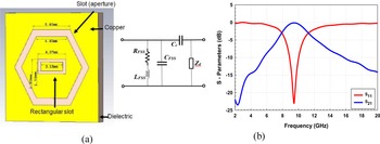
First, a hexagonal aperture loop-based unit cell is designed with a rectangular-shaped slot element at the center of the unit cell (Fig. 2(a)). This slot essentially disturbs the continuous surface current distribution and hence contributes to controlling scattering characteristics of the designed superstrate. Here, the substrate is RT Duroid 5880, with the dimensions 13.44 mm × 13.44 mm, and the thickness of 1.59 mm. According to the HIS specifications, the resonance can be achieved when the circumference (perimeter) of the loop is equal to the operating wavelength. The S-parameters of the unit cell is presented in Fig. 2b. The resonant frequency of the unit cell is 9.416 GHz with a reflection coefficient of −23.88 dB. The equivalent circuit of the unit cell is also included in the figure. Essentially it is a parallel RLC circuit [Reference Ghosh and Srivastava17] whose surface impedance is expressed as Zs = ZFSS II (Zd + 1/jωCc). Here, ZFSS = RFSS + jωLFSS + 1/jωC FSS; Zd includes the dielectric losses of the substrate, and Cc is the coupling capacitance of the hexagonal aperture loop and the rectangular slot. Further, it is well-known that metamaterial (MTM) can be used to design high-performance absorber with minimum possible thickness. The electric and magnetic resonances of MTM unit cell can be tuned by varying its dimensions. Further, the absorbance bandwidth of MTM can be enhanced by combining unit cell structures of different dimensions into a co-planar unit cell [Reference Lee and Lee18]. Likewise, in the proposed design, a unit cell for MTM layer is designed using a rectangular loop of four different sizes to achieve good absorption over wide frequency range, when inserted in the antenna design in lieu of multi-resonance effect.
Hexagonal aperture loop structure with rectangular slot: (a) unit cell, (b) S-parameters.

Design of superstrate
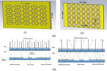
The designed superstrate, shown in (i) of Fig. 3(a) comprised of 5 × 5 array of unit cells designed on 67.2 × 67.2 × 1.59 mm substrate for a single patch antenna. Figure 3(a) (ii) presents a superstrate having 7 × 5 array of unit cells designed on 90 mm × 40 mm × 1.59 mm substrate for a 4-element linear patch array. The unit cells in the two cases are different, the details of which are explained in subsequent sections. The working mechanism of the superstrate has been explained in Fig. 3(b), where the incident and scattered EM wave are shown. The thick arrows in different grey scales represent impinging waves of different frequencies, whereas thin arrows represent the scattered/transmitted/refracted waves. It is to be noted that the incident wave of different frequency would have different scattering effect. A portion of out-of-band EM wave gets absorbed by the partially absorbing surface (PAS), which is the top layer of superstrate. Another portion is reflected back by partially reflecting surface (PRS) which is the bottom layer of the superstrate (only in three-layered configuration). The in-band EM waves would transmit through the superstrate and strike the patch antenna and MA layer (present only in three-layered configuration). These in-band frequencies will be absorbed or diffracted to other directions in MA layer. When patch antenna radiates, the radiated waves can undergo multiple reflections within the cavity formed by the antenna and superstrate layers, thereby contributing toward gain improvement. Further the HIS-based hybrid ground plane of the patch array also contributes toward out-of-band RCS reduction.
(a) Superstrate configurations: (i) for single patch antenna, (ii) for four-element linear patch array, (b) working principle of superstrate-based antenna: (i) incident EM wave, (ii) scattered/ radiated EM wave (reflection, refraction, transmission, absorption).

Single patch antenna with superstrate
Single patch antenna with superstrate (two-layered)
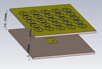
The dimension of the designed patch antenna is 9.07 mm × 11.86 mm. The antenna is fed by a coaxial feed, as shown in Fig. 4. The periodic structure-based superstrate (Fig. 3(a)) is placed over the patch antenna. The dimension of the superstrate is 67.2 mm × 67.2 mm × 1.59 mm, which is the same as the substrate of the antenna.
A single patch antenna with periodic structure-based superstrate (two-layered configuration).

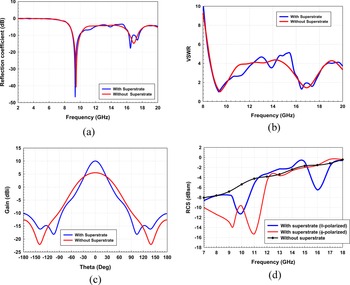
The superstrate has an upper layer designed with hexagonal aperture loops arranged periodically. It is noted that superstrate does not have PRS layer at the lower side. The distance between the superstrate and the antenna is optimized to 16.5 mm (greater than half-wavelength, f o = 9.47 GHz). Here, for a single patch antenna the superstrate consists of 5 × 5 array of unit cells. The inter-element spacing between the unit cells is 0.65 mm in the vertical direction and 1.2 mm in the horizontal direction. Rectangular loops have been introduced in the center of the unit cells. The outer and inner length of the loop is 4.07 and 3.15 mm, respectively. On the other hand, the outer and inner breadth of the loop is 1.8 and 1.1 mm, respectively. The overall comparison of the performance of a single patch antenna with and without superstrate is given in Table 1. It can be observed from Fig. 5 that the radiation as well as scattering characteristics of the patch antenna has improved when superstrate is included in the design. A single patch antenna was resonating at 9.47 GHz with reflection coefficient of −39.83 dB and VSWR equal to 1.02.
Performance of a single patch antenna with superstrate (two-layered): (a) reflection coefficient, (b) VSWR, (c) gain, (d) structural RCS.

Performance of a single patch antenna with superstrate.

On the other hand, the antenna with superstrate configuration resonates at 9.36 GHz with reflection coefficient of −46.6 dB, as shown in Fig. 5(a). The VSWR value of the antenna is 1.009 and 1.02, with and without superstrate at resonant frequencies, respectively (Fig. 5(b)). The gain of patch antenna without superstrate is 5.51 dBi, which increased to 10 dBi (Fig. 5(c)) when the superstrate is included in antenna structure. The structural mode RCS of patch antenna is reduced from −6.259 dBsm at f o = 9.47 GHz (without superstrate) to −8.63 dBsm at f o = 9.36 GHz (with superstrate) for θ-polarized plane wave and to −13.6 dBsm (with superstrate) for ϕ-polarized plane EM wave. The maximum reduction in RCS is observed at 11 GHz with structural RCS of −15.3 dBsm for ϕ-polarized plane wave incidence. In other words, the RCS of patch antenna is reduced by 11.4 dBsm, as shown in Fig. 5(d). In order to further improve the extent of RCS reduction, the three-layered configuration of the superstrate has been attempted.
A single patch antenna with superstrate (three-layered)
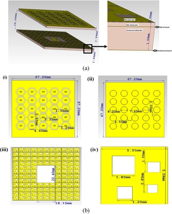
The three-layered structure consists of patch antenna, superstrate with PAS and PRS layers as upper and lower layers, respectively, and the MA. The PAS layer is the periodic arrangement of hexagonal aperture unit cells and the PRS layer is designed with a periodic arrangement of circular loops. The superstrate configuration is considered as the first layer. The distance between the superstrate and the patch antenna is optimized to 16.5 mm. The patch antenna is surrounded by a MA layer. It is noted that the ground plane of the MA is co-planar with patch antenna. The MA layer consists of rectangular-shaped metamaterial unit cells with slots, arranged periodically, which constitutes the second layer.
The single patch antenna (11.86 mm × 9.07 mm) is the third layer. The schematic of the configuration with dimensions is shown in Fig. 6. The significance of the PAS layer is to absorb the out-of-band frequencies and let in the in-band (X-band) frequencies, whereas the PRS layer is to reflect the part of out-of-band frequencies that penetrate through the PAS layer and also band-pass in-band frequencies [Reference Meng, Li, Fan, Li, Xue, Chen and Wua15]. The combination of all these layers, i.e., superstrate with PAS and PRS layers and patch antenna with MA contributes to partially reflecting and absorbing surface (PRAS) antenna. Therefore, the PAS and PRS layers will reduce out-of-band RCS and the MA contributes to reduce in-band RCS [Reference Mu, Wang, Wang and Huang4].
(a) A single patch antenna with superstrate (three-layered). (b) Details of superstrate: (i) PAS layer (upper part of layer 1), (ii) PRS layer (lower part of layer 1), (iii) MA (layer 2) co-planed on single patch antenna, (iv) unit cell of MA.

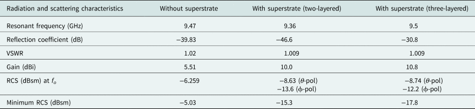
The comparison of the performance of a single patch antenna with and without periodic structure-based superstrate (three-layered configuration) is shown in Fig. 7. The single patch antenna resonates at 9.47 GHz and the reflection coefficient is −39.83 dB. On the other hand, when periodic structure-based superstrate (three-layered) is included in the antenna structure, the resonance frequency shifts to 9.5 GHz with a reflection coefficient of −30.8 dB (Fig. 7(a)). The VSWR of the patch antenna is 1.009 and 1.05 with and without superstrate at resonant frequencies, respectively (Fig. 7(b)). The antenna gain without superstrate is 5.51 dBi, and increases to 10.8 dBi at the resonant frequency when superstrate is added (Fig. 7(c)). It is noted that the gain of a single patch antenna has improved by 5.29 dB when periodic structure-based superstrate is included (three-layered configuration). The structural mode RCS of a single patch antenna is reduced from −6.259 dBsm at f o = 9.47 GHz (without superstrate) to −8.74 dBsm at f o = 9.5 GHz (with superstrate) for θ-polarized plane wave incidence. The maximum RCS reduction (~10 dB) is observed at 11 GHz for θ-polarized incidence. Almost similar trend (or even better) in RCS reduction is observed for ϕ-polarized incident EM wave. The minimum antenna RCS of −17.8 dBsm (ϕ-polarized) is achieved for this configuration. Further, the RCS reduction bandwidth has increased for a three-layered structure as compared to a two-layered structure. Table 1 presents the comparison of radiation and scattering characteristics of a single patch antenna without and with superstrate for both two-layered and three-layered configurations. It shows that the antenna performance is almost similar in both the cases. However, this is not the case when the four-element patch array is considered.
Performance of a single patch antenna with superstrate (three-layered): (a) reflection coefficient, (b) VSWR, (c) gain, (d) structural RCS.

Patch array with superstrate
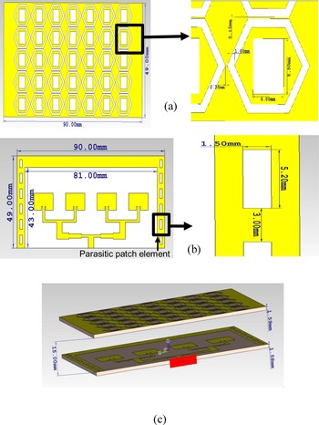
Next, a periodic structure-based superstrate is designed for four-element linear patch array. The dimension of each patch is 9.07 mm × 11.6 mm and the inter-element spacing between each element is greater than 0.5λ. The antenna is fed by a corporate feed network. The dimension of both the substrate and the superstrate is 49 mm × 90 mm × 1.58 mm. A rectangular slot (4 mm × 5.5 mm) is cut at the center of the unit cell. The superstrate is designed with 7 × 5 array of unit cells. The inter-element spacing in the vertical and horizontal direction in between the unit cells is kept 0.15 and 0.2 mm, respectively.
A four-element linear patch array with superstrate (two-layered)
The two-layered structure consists of patch array and superstrate. The superstrate is designed with the periodic arrangement of hexagonal aperture unit cells as the upper layer. The ground of the patch array is designed as the reduced ground plane having square patches and JC elements [Reference Singh and Singh2]. The distance between the superstrate and the antenna is optimized to 15 mm. Parasitic patch elements have been placed on the antenna substrate, i.e., coplanar to the patch array. The electromagnetic energy is coupled from the driven patch array to parasitic patch elements via both the space and the surface waves. The far-field radiation pattern of patch array gets improved on the addition of parasitic elements around the patch array elements [Reference Ta, Kedze, Chien and Park19]. The structure of the antenna with a periodic structure-based superstrate is shown in Fig. 8.
A four-element patch array with periodic structure-based superstrate in two-layer configuration: (a) PAS layer of the superstrate, (b) four-element linear patch array with parasitic patch, (c) patch array with superstrate.

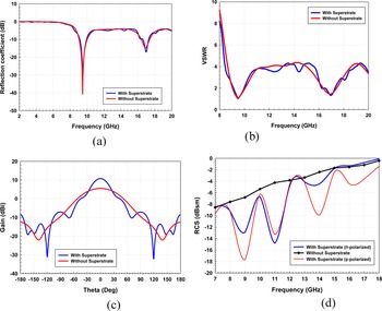
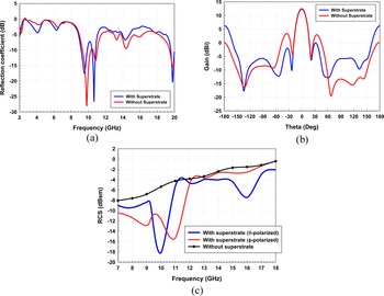
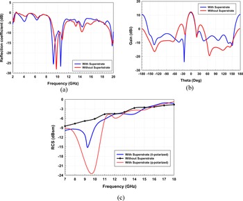
The radiation and scattering parameters of this configuration are compared with the conventional patch array in Fig. 9. The resonant frequency of the patch array with the conventional PEC ground plane is 9.787 GHz, with a reflection coefficient of −30.57 dB. On the other hand, patch array with periodic structure-based superstrate (two-layered configuration) resonates at 9.55 and 10.65 GHz with a reflection coefficient of −17.5 and −26.5 dB, respectively (Fig. 9(a)). The VSWR of patch array without superstrate is 1.09 at the resonant frequency, and for patch array with superstrate it is 1.13 at 9.55 GHz and 1.09 at 10.65 GHz. The gain of the patch array without superstrate is 12.3 dBi, which became 12.5 dBi at 9.55 GHz when the superstrate is used (Fig. 9(b)). However, there is an increase in backside radiation when superstrate is included. The backside radiation may be caused by the surface waves in periodic structures (used in superstrate design). This might degrade the antenna efficiency. The reported solutions for the backside radiation from antennas is inclusion of corrugations over the surface, or soft surfaces comprising of metal strips and grounded vias [Reference Ronglin, DeJean, Tentzeris, Papapolymerou and Laskar20, Reference Iglesias, Sánchez and Teruel21]. Further, it can be observed from Fig. 9(c) that the structural RCS of four-element linear patch array is reduced from −6.36 dBsm at f o = 9.787 GHz (without superstrate) to −10.54 dBsm at f o = 9.55 GHz (with superstrate) for θ-polarized plane wave incidence. The RCS reduction is well-evident even for ϕ-polarized incidence, similar to single patch antenna with two-layered superstrate (Fig. 5(d)). The maximum RCS reduction (12.13 dBsm) is observed at 10 GHz for θ-polarized incidence. The structural mode RCS of patch array with two-layered superstrate is −18.33 dBsm at 10 GHz for ϕ-polarized incident EM wave.
Performance of four-element linear patch array with superstrate: two-layered configuration, (a) reflection coefficient, (b) gain, (c) structural RCS.

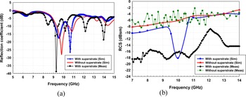
The designed four-element patch array with periodic structure-based superstrate (two-layered configuration) is fabricated using a PCB prototyping machine. The radiation and scattering performances of the fabricated antenna are measured (Fig. 10) and compared with the simulated results. Figure 11 presents the measured reflection coefficient and the structural RCS. The measured resonant frequencies of patch array with superstrate are 9.29 and 10.19 GHz with a reflection coefficient of −38.83 and −13.14 dB, respectively. The simulated VSWR of the patch array with superstrate obtained at 9.55 GHz is 1.3 and at 10.65 GHz is 1.09. On the other hand, the measured VSWR at 9.29 GHz is 1.02 and at 10.19 GHz is 1.16. The simulated gain of patch array with periodic structure-based superstrate at 9.55 GHz is 12.5 dBi, while the measured gain of patch array with superstrate obtained is 12.33 dBi.
Measurement setups for fabricated four-element linear patch array with superstrate (two-layered configuration). (a) Reflection coefficient and VSWR, (b) gain, (c) structural RCS, (d) fabricated superstrate and patch array.

Measured performance of four-element linear patch array with superstrate (two-layered): (a) reflection coefficient, (b) structural RCS.

In Fig. 11(b), the structural RCS (simulated and measured) of a superstrate-based patch array for θ-polarized plane wave incidence is compared with the patch array without superstrate. It can be observed that the measured structural RCS of the fabricated antenna is reduced significantly over the entire X-band which corresponds to the in-band frequencies of the antenna considered. The patch array dimension is relatively small (4.9 cm × 9 cm) compared to the measurement facility. Firstly, for such a small structure, the edges will scatter more than the antenna surface for even a slight variation in the azimuth plane. The scattering from the edges and the boundaries of the patch antenna array would be absorbed in the anechoic chamber, and thus shows smaller RCS as compared to the simulated one.
A four-element linear patch array with superstrate (three layered)
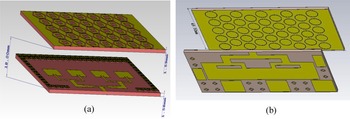
A four-element patch array with a three-layered superstrate has been designed. This configuration consists of superstrate (with upper PAS layer and lower PRS layer), MA layer and four-element linear patch array. The distance between the superstrate and the antenna is optimized to 18 mm. The MA layer consists of metamaterial unit cells, MA substrate and MA ground. The metamaterial unit cells comprised of two rectangular loops arranged periodically. The patch array (layer 3) is surrounded by this layer and shares the same plane with the ground of this second layer. The MA layer is placed at the edges of the patch array substrate. Care is taken in maintaining proper space for the patch array to achieve good radiation performance. Figure 12 shows the details of this configuration of four-element linear patch array with periodic structure-based superstrate (three-layered configuration).
Four-element patch array with periodic structure-based superstrate (three-layered configuration). The antenna array is surrounded by MA. (a) Top view of patch array and superstrate, (b) bottom view of patch array and superstrate.

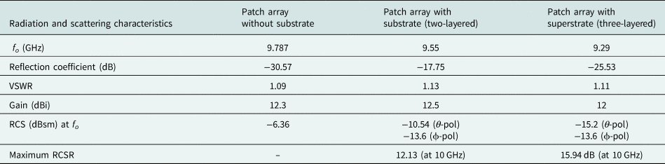
The comparison of the radiation and scattering performances of four-element patch array with and without periodic structure-based superstrate (three-layered configuration) is presented in Table 2. Figure 13 presents the comparison of the performance of patch array with and without superstrate. The resonant frequency of the configuration is 9.29 GHz with a reflection coefficient of −25.53 dB. The obtained VSWR and gain at the resonant frequency is 1.11 and 12 dBi, respectively. The structural mode RCS of patch array is −15.2 dBsm at 9.29 GHz for θ-polarized plane wave incidence. It can be observed that array RCS is reduced significantly at a resonant frequency of 9.29 GHz from −6.36 to −15.2 dBsm. In case of ϕ-polarized incidence, the minimum structural RCS is −22.2 dBsm at 10 GHz. The array RCS is reduced in entire X-band for both the polarizations, with optimum radiation performance in terms of the reflection coefficient, gain, and VSWR.
Performance of four-element patch array with periodic structure-based superstrate: three-layered configuration: (a) reflection coefficient, (b) gain, (c) structural RCS.

Performance of four-element patch array with superstrate.

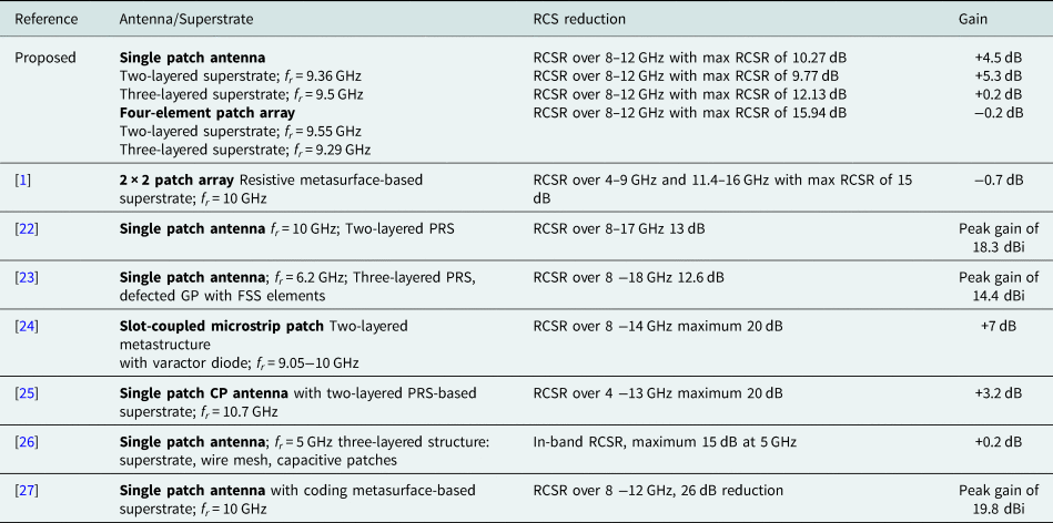
This configuration lags behind the two-layered configuration of superstrate-based patch array, in view of the complicated design and hence fabrication issues. The performance of two-layered superstrate-based patch array design is broadly good both in terms of radiation and scattering than the three-layered one. In addition, the configuration is simple to fabricate. Table 3 presents the comparison of the performance of the proposed configurations with that earlier reported in the open domain. It can be observed that most of the reported designs [Reference Jiang, Xue, Li, Ren and Cao22–Reference Zhang, Wan, Liu, Yin, Zhang, Wu and Cui27], are of single patch antenna with superstrate. It is true that these designs show significant RCS reduction with good radiation characteristics. However, actual airborne and ground-based radar systems have large phased arrays. Thus, study based on a single patch fed by a coaxial feed would not be helpful in controlling array RCS. Moreover, the superstrate needs to analyze for the array or at least sub-array configurations with appropriate feed structure. In many radar systems, four-element patch arrays are used as sub-array. In [Reference Chen, Guo, Sang, Sun and Fu1], it is reported that 2 × 2 patch array with superstrate shows RCS reduction but with gain loss. On the other hand, the proposed configuration in this paper has a four-element patch array with a superstrate. It shows RCS reduction for X-band frequencies without degrading the antenna performance.
Comparison of the performance of proposed configuration with the reported ones

Conclusion
The major challenge in designing low observable antennas is reduction in antenna scattering without any degradation in its radiation performance. A periodic structure-based superstrate is included in the design of four-element patch array in two-layered and three-layered configurations. The ground of the array is designed as a reduced ground plane having two types of HIS-elements in the form of patch and JC. In both configurations, the array gain of 12.5 dBi is maintained broadly with a reduction in structural RCS over the entire in-band frequencies of X-band. The reflection coefficient (~ −20 dB) and VSWR (~ 1.1) of the array are also maintained in an acceptable range. Moreover, in view of simplicity in fabrication, the two-layered configuration of the superstrate presents a better option for low RCS antenna array. The proposed superstrate-based patch array design shows a significant reduction of 12 dB (approx.) in in-band antenna RCS without any degradation in its radiation characteristics. Such low RCS configurations can be used as subarray of larger phased arrays in airborne, naval, and ground-based radar applications.
Acknowledgments
We express our thanks to Mr. K.S. Venu and Mr. Ajith Nair of CEM, CSIR-NAL for the antenna measurements. We would also like to thank Prof. Dharmendra Singh of ECE Department of IIT, Roorkee for RCS measurements. We are grateful to Aeronautics Research and Development Board (DRDO-AR&DB) of India for the financial support.
 S. K. Vyshnavi Das worked as project assistant in the Centre for Electromagnetics of CSIR-National Aerospace Laboratories, Bangalore, India. She obtained M.Tech. in electronics & communication engineering, Pondicherry Central University, India in 2018. She did her B.Tech in electronics and communication engineering from GECW, Kannur University, India in 2015. Her research areas include radar cross section (RCS) studies, and EM design and analysis of low-profile phased arrays.
 Avinash Singh is a research scholar in the ECE department of IIT Roorkee, Uttarakhand, India. He has obtained integrated B.Tech. and M.Tech. (electronics and communication) from Amity University, Jaipur, India in 2016. He worked as project assistant at the Centre for Electromagnetics (CEM) of CSIR-National Aerospace Laboratories, Bangalore. His research interests are RF devices/components, active RCS reduction, estimation and control of RCS of phased arrays, multi-layered radar absorbing structures (RAS), and millimeter wave antenna arrays. He has co-authored one book, one book chapter, 10 research papers, 25 technical documents, and test reports.
 Arti A. Gurap worked as project assistant in the Centre for Electromagnetics of CSIR-National Aerospace Laboratories, Bangalore, India. She obtained M.Tech. in microwave engineering, Pune Institute of Computer Technology, Savitribai Phule Pune University, India in 2018. She did her B.Tech in electronics and communication engineering from Vishwabharati Academy College of Engineering, Pune in 2016. Her research areas include low observable phased arrays and millimeter wave antenna arrays.
 Hema Singh is currently working as senior principal scientist in the Centre for Electromagnetics of CSIR-National Aerospace Laboratories, Bangalore, India. She was faculty in the EEE group of Birla Institute of Technology & Science (BITS), Pilani during 2001–2004. She obtained her Ph.D. degree in electronics engineering from IIT-BHU, Varanasi, India in 2000. Her active area of research is computational electromagnetics for aerospace applications, EM analysis of propagation in an indoor environment, phased arrays, conformal antennas, RCS studies including active RCS reduction. She is senior IEEE member and received an award of IEEE Women Technologist of the Year 2020 by IEEE Bangalore chapter. She was also awarded IETE Smt. Ranjana Pal award in 2018 for her contributions in the area of active RCS reduction. Dr. Singh has co-authored 15 books, two book chapters, seven software copyrights, and over 390 research papers and technical reports.