Introduction
The first 5th generation (5G) mobile network was rolled out in South Korea in 2019. Compared to the previous generations, 5G provides much higher capacity and lower latency to meet the requirements of ever-increasing data rate, number of connected devices, and emerging applications. To achieve this, wider bandwidth and more frequency bands have been assigned to 5G including sub-6 GHz bands and millimeter-wave (mm-wave) bands such as 26–30 GHz [Reference El-Halwagy, Nag, Hisayasu, Aryanfar, Mousavi and Hossain1, Reference Azim, Meaze, Affandi, Alam, Aktar, Mia, Alam, Samsuzzaman and Islam2]. Although mm-wave can provide a chunk of continuous bandwidth up to GHz, only a few countries have adopted it in reality; most deployed 5G networks are running at sub-6 GHz bands. One of the major challenges for deploying mm-wave 5G lies in the immature technology for frontends, causing low gain, low power efficiency, and high cost. Low-noise amplifiers (LNAs) are critical components in the frontend of all communication systems usually located at the first stage of the receiver after the antenna. Typical semiconductor technologies for LNAs are divided into two categories: silicon and III–V compound. The former includes complementary metal oxide semiconductor (CMOS), silicon germanium bipolar complementary metal oxide semiconductor (SiGe BiCMOS), and silicon on insulator which have the advantages of low power consumption, high integrability, low cost, and compact size but is poor with regard tonoise figure (NF) and gain [Reference Mendes, Vaz, Passos, Lourenço and Martins3, Reference Xu, Schumann, Ferschischi, Finger, Carta and Ellinger4]. The latter consists of conventional Indium phosphide (InP) [Reference Tang, Wadefalk, Morgan and Weinreb5] and gallium arsenide (GaAs) [Reference Wang, Chen, Liu, Mo, Chen, Wang and Yu6] high electron mobility transistors (HEMTs) which have lower NF and higher gain than the silicon technologies. More recently, gallium nitride (GaN) HEMTs have received great attention for their excellent performance in both low noise and high power [Reference Tong, Zhang, Zheng, Zhang, Xu and Wang7–Reference Kobayashi, Denninghoff and Miller9]. Compared with GaAs and InP, one of the significant advantages of GaN LNAs is their high-power handling capability which is preferable in complex electromagnetic environments, e.g., remote sensing in space or satellite communications, where additional measures, such as limiters, must be implemented to protect the receivers. In addition, the high-power tolerance ability is also desirable in signal detection and electronic countermeasure and multiple input multiple output communications [Reference Tong, Zhang, Zheng, Zhang, Xu and Wang7].
In this work, we demonstrate a three-stage monolithic integrated GaN LNA operating between 26 and 29 GHz for mm-wave 5G applications. Unlike GaN LNAs reported elsewhere [Reference Zheng, Zhang, Xu, Wang and Tong10, Reference Rudolph, Chaturvedi, Hirche, Wurfl, Heinrich and Trankle11], the LNA demonstrated here has three stages and is powered by a single power supply. Such a design simplifies biasing circuits and makes the whole circuit more compact. The measured gain and 1 dB compression point output power (P 1dB) are 30.5 ± 0.4 dB and 21 dBm, respectively. The NF is 1.65–1.8 dB in 26–29 GHz. The measured S 11 and S 22 are both below −10 dB across the whole band. The results show the proposed GaN LNA could be an ideal candidate for mm-wave 5G.
LNA design
The HEMT and its small-signal model
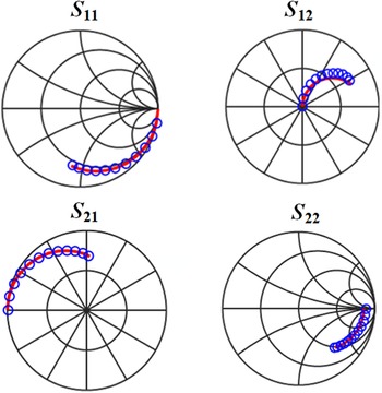
The GaN transistor used in this work is 2 × 30 μm and is developed using a 0.1 μm depletion mode. Figure 1 shows its small signal equivalent circuit. The initial bias conditions of the device were chosen to achieve the maximum value of fT × gm/IDS, where fT, gm, and IDS are transition frequency, transconductance, and source-drain current, respectively [Reference Schleeh12–Reference Teng15]. However, the ultimate optimal bias voltages at the gate, Vg, and the drain, Vd, are −2 and 15 V, respectively. They were decided as a compromise among matching loss, NF, gain, and stability. In order to match the input impedance (Zin) of the LNA to 50 Ω, an inductive degeneration was adopted, making the real part of Zin equal to 2πLseff + Rs, where Lseff is the effective source or emitter inductance and Rs is the source resistance. The measured S-parameters of the transistor are shown in Fig. 2 and extracted values of the small-signal equivalent circuit are shown in Table 1. The simulated results based on the model are in good agreement with the measured ones.
The small-signal equivalent circuit of GaN HEMT when being biased at Vg = −2 V and Vd = 15 V.

The measured (blue circle) and modeled (red line) S-parameters. The frequency range is from 0.2 to 60 GHz.

Extracted intrinsic small-signal parameters of the GaN HEMT

LNA design
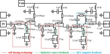
In this work, we used a common source cascaded three-stage architecture to achieve a minimum gain of 30 dB, which is higher than the state of art LNAs operating in the same frequency range, while keeping NF as low as possible as shown in Fig. 3. The overall NF in a cascaded system is determined by the well-known Friis equation

where NFx and Gx (x = 1, 2, 3) are NF and gain of the xth stage of the cascaded LNA in a linear scale. The gain and NF of the first stage are more important than those of the following stages. Since HEMTs are constructed in a common source topology and the same HEMTs are used for all stages, the main task is then focused on input matching for minimizing the NF and lowering the input return loss at the first stage. The final stage serves the purpose of maximizing gain, improving the flatness of the gain, and reducing output return loss. A series RLC negative feedback loop, highlighted in blue in Fig. 3, is applied between the gate and drain of the third stage to adjust the gain flatness and improve the stability. However, its contribution to the overall NF is very limited as seen in (1). The inter-stage is tuned to ensure noise, gain, and input and output standing wave ratio meet the overall goal. A feedback inductor was deployed at the source of the HEMT, to achieve minimum NF and low input return loss simultaneously as highlighted in green in Fig. 3. Adding this inductor at the first stage will rotate S 11 of the LNA close to the optimum reflection coefficient Гopt for noise [Reference Zheng, Zhang, Xu, Wang and Tong10] and achieve both optimal noise matching and input conjugate matching [Reference Axelsson and Andersson16]. Finally, the inductive source feedback can also improve the stability. Although the inductive degeneration does not have the same impact on the NF as resistive degeneration does, it still reduces the overall gain of the circuit.
Simplified schematic of the designed LNA.

Biasing circuit
A self-biasing technology is utilized to power all HEMTs conveniently through a single drain voltage, providing greater flexibility of biasing conditions [Reference Wang, Hou, Chen, Chen, Yan, Zhang and Hong17, Reference Qi and He18]. As highlighted in red in Fig. 3, the circuit contains a shunt resistor (R) and capacitor. The capacitor acts as a bypassing capacitor, helping to filter out noise contribution from the feedback resistor and improve the gain at the interested frequency range. The negative voltage on the resistor (R) is supplied to the gate through the grounded microstrip of the input matching circuit that, as part of source impedance matching, simplifies the input matching network, thus Vg can be expressed as −IDS × R. In the proposed LNA, IDS and R are 25.9 mA and 77 Ω, respectively, when it is biased at Vg = −2 V and Vd = 15 V. Although careful design and several iterations of process validation have been made, the process variation may still affect the self-biasing circuit. In fact, we implemented a laser trimming on the resistor for fine-tuning. It should be noted that, due to the presence of the capacitor, much more care should be taken for stability simulation. A quarter-wavelength stub with a resonant capacitor and a resistor in the drain bias line is used as a radio frequency (RF) choke for stability improvement at each stage. Furthermore, the whole circuit has only two bonding pads for the drain, which can largely ease bonding and packaging. The overall bias circuits are more favorable for practical applications.
Measurements and discussion
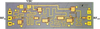
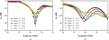
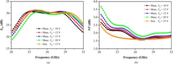
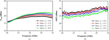
Figure 4 shows the fabricated monolithic microwave integrated circuit (MMIC) LNA that has an area of 0.8 × 2.4 mm2. Although −2 and 15 V are required for gate and drain of the HEMT, only 15 V was needed because a self-biasing technology was adopted. S-parameter measurements were made on chip with ground-signal-ground probes at room temperature and the results are shown in Figs 5 and 6. As can be seen, the measured S 11 and S 22 are below −10 dB between 26 and 29 GHz, indicating that both the input and output matching are good. Moreover, the measured gain is 30.5 ± 0.4 dB in the same frequency range. The simulated results are also plotted against the experimental results, and good agreements have been achieved. The cold source method was used to measure NF and both the experimental and simulated results are shown in Fig. 6(b). One can notice that the measured NF is between 1.65 and 1.8 dB in the band, and the discrepancy between the measurement and simulation is smaller than 0.3 dB. The linearity of the LNA was also investigated and the results are shown in Fig. 7. The measured P 1dB and third-order intercept point output power (OIP3) are approximately 21 and 27 dBm, respectively, which are much higher than GaAs and InP LNAs. Figure 8 shows the measured gain and output power versus input power at 28 GHz when the LNA is biased at Vd = 15 V. Note that the measured OIP3 and the results in Fig. 8 were obtained after the chip was packaged, which are slightly lower than the results obtained by on-chip measurements due to bondwire and packaging.
Photograph of the fabricated LNA.

Measured and simulated S 11 (a) and S 22 (b) of the LNA at different bias points.

Measured and simulated S 21 (a) and NF (b) of the LNA at different bias points.

Measured P 1dB (a) and OIP3 (b) of the LNA at different bias points.

Measured gain and output power versus input power at 28 GHz (Vd = 15 V, with RF and direct current (DC) pads bonded to the test board).

The analysis of the fabricated LNA is also performed at different bias points (10–20 V) as shown in Figs 5–7. It is observed that the device performs better in terms of return loss and gain at lower drain voltage and the gain ripple remains the same for all the cases. The designed LNA gives promising results to all four bias conditions. It is noticed that the LNA can accommodate a wide range of supply voltages from 10 to 20 V, which is preferred in radar systems in practice.
We compared the performance of the designed LNA with recently published LNAs using different semiconductor technologies for mm-wave 5G and the results are summarized in Table 2. We can observe that NF of this work is comparable with InP LNAs, even better than GaAs and CMOS. Moreover, it is noteworthy that the single power supply employed in this work can ensure a competitively excellent performance compared with the other works powered by dual sources using the same technique. It is known that the main drawback of the self-biasing technique is sacrificed gain and NF. In addition, this LNA has a relatively high and flat gain as well as a high P 1dB of 21 dBm compared to GaAs and InP LNAs. Meanwhile, the high linearity sacrifices the power consumption but is still much higher than LNAs using other technologies. The measured NF is slightly higher than that of other LNAs based on 0.1 μm GaN process due to the resistors in the self-biasing circuits. However, the adopted self-biasing structure simplifies external circuitry.
Comparisons of LNAs for mm-wave 5G using different semiconductor technologies

Conclusion
A GaN LNA based on 0.1 μm GaN MMIC process operating at 26–29 GHz is demonstrated in this work. The single powered LNA has a high and flat gain of 30.1–30.9 dB and good input and output matching. The NF is 1.65–1.8 dB in the band. The LNA has good linearity with P 1dB close to 21 dBm. Compared with the published LNAs, the LNA demonstrated in this work exhibits a competitive NF and a relatively high and flat gain as well as high linearity. In addition, this single powered LNA provides ease of use and simplifies the overall system on account of the powering method compared to that of the individually powered LNA. To our knowledge, the combination of NF, gain, and linearity performance represents the state of art of self-biased LNAs suitable for mm-wave 5G communications.
Acknowledgements
This work was supported in part by the National Natural Science Foundation of China (NSFC) under Grant 61804077, and in part by the Jiangsu Science and Technology Department under Grant BE2019116.
 Yi Wang is currently pursuing the Ph.D. degree with the Nanjing University of Science and Technology, Nanjing, China. From January 2019 to July 2019, she was a Visiting Researcher with the Department of Electromagnetic and Electrochemical Technologies at the National Physical Laboratory, Teddington, U.K., where she was involved in high-frequency electromagnetic measurement. From January 2021 to present, she is a Visiting Scholar with the Microwave and Terahertz Electronics Research Group at the University of Glasgow, working on the MMICs design. Her current research interests include high-frequency electromagnetic measurement, MMICs, and microwave and terahertz components.
 Tongde Huang received the Ph.D. degree from the Department of Electronic and Computer Engineer, Hong Kong University of Science and Technology, Hong Kong, in 2013. From 2014 to 2016, he was a Research Fellow with Chalmers University of Technology, Gothenburg, Sweden. From 2016 to 2017, he was a Researcher with the Microwave Electronics Laboratory, Chalmers University of Technology, Gothenburg, Sweden. Currently, he is an Associated Professor with the School of Electronic and Optical Engineering, Nanjing University of Science and Technology, Nanjing, China. His current research interests are GaN RF devices and MMICs.
 Saisai Jin received the M.S. degree from the University of Electronic Science and Technology of China, Chengdu, China, in 2019. He is currently working with Nanjing Guobo Electronics Co., Ltd, Nanjing, China. His research interests include RF and millimeter-wave integrated circuits for wireless communication systems.
 Chong Wang received the Ph.D. degree in circuits and systems from Southeast University, Nanjing, China, in 2016. From 2016 to 2018, he was an RFIC designer in the department of Monolithic circuits in CETC 55 Institute. Currently, he is an MMIC engineer in Nanjing GuoBo Electronics Co., Ltd, Nanjing, China. His current research interests include RF and millimeter-wave integrated circuits for wireless communications and phased-array systems based on Silicon and compound semiconductors.
 Dongdong Ma was born in Henan Province, China, in November 1989. He received the B.S. degree and the M.S. degree from Xinyang Normal University. He is currently working toward the Ph.D. degree with the Nanjing University of Science and Technology, Nanjing, China. His current research interests include microwave and millimeter-wave components, circuits, and measurement.
 Hongchang Shen received the B.S. degree from the University of Electronic Science and Technology of China, Chengdu, China, in 2002, and the M.S. degree from the Nanjing University of Science and Technology, Nanjing, China, in 2013. He is currently working with Nanjing GuoBo Electronics Co., Ltd, Nanjing, China. His research interests include RF and millimeter-wave integrated circuits, and phased-array transceiver design.
 Chong Li obtained his Ph.D. from the University of Glasgow in 2012. In 2011, he became a Post-Doctoral Research Associate with the University of Glasgow, working on the development of millimeter-wave signal sources and terahertz imaging systems. In January 2014, he joined the National Physical Laboratory (NPL), Teddington, U.K., as a Higher Research Scientist, where he contributed to and led several commercial projects and U.K. national and European research projects. He was the Measurement Service Provider (MSP) of the ultrafast waveform metrology service at NPL. He also led work on microwave and millimeter-wave on-wafer measurements. In August 2017, he returned the University of Glasgow, where he is a Senior Lecturer and currently leading the Microwave and Terahertz Electronics Research Group. He has published more than 80 journal and conference papers and 3 patents. His current research interests include MMICs, microwave and terahertz components, systems and metrology, and next-generation wireless communications.
 Yuehua Li was born in Jiangsu, China, in 1959. He received the B.S., M.S., and Ph.D. degrees in electronic engineering from the Nanjing University of Science and Technology, Nanjing, China, in 1982, 1989, and 1999, respectively. He is currently a Professor with the School of Electronic Engineering and Optoelectronic Technology, Nanjing University of Science and Technology. His research interests include target recognition, signal processing, and detection technology.
 Wen Wu received the Ph.D. degree in electromagnetic field and microwave technology from Southeast University, Nanjing, China, in 1997. He is currently a Professor with the School of Electronic Engineering and Optoelectronic Technology, Nanjing University of Science and Technology, where he is also the Associate Director with the Ministerial Key Laboratory of JGMT. He has authored or coauthored over 300 journal and conference papers and has submitted over 30 patent applications. His current research interests include microwave and millimeter-wave theories and technologies, microwave and millimeter-wave detection, and multimode compound detection. He was a recipient of the Ministerial and Provincial-Level Science and Technology Awards for six times.