I. INTRODUCTION
Nanocomposite films consisting of one amorphous phase and one or more nanocrystalline phases can exhibit very high hardness. This has been explained by hindering of dislocation motion by the thin amorphous matrix surrounding the crystallites.Reference Veprek and Reiprich1 Hard nanocomposites of several material systems have been studied, e.g., Ti–Si–N,Reference Veprek and Reiprich1, Reference Veprek, Niederhofer, Moto, Bolom, Männling, Nesladek, Dollinger and Bergmaier2 Ti–Si–C–N,Reference Ma, Ma and Xu3, Reference Guo, Ma and Xu4 Zr–Si–N,Reference Winkelmann, Cairney, Hoffman, Martin and Bendavid5 and Ti–B–N.Reference Mitterer, Losbichler, Hofer, Warbichler, Gibson and Gissler6, Reference Karvankova, Veprek-Heijman, Zindulka, Bergmaier and Veprek7 Such nanocomposites also retain their hardness at high temperatures since the grain growth is hindered by the amorphous matrix.Reference Männling, Patil, Moto, Jilek and Veprek8 Also two-phase nanocrystalline materials in the form of multilayers exhibit an increased hardness compared to their constituents due to the difference in elastic properties between the layers that hinder dislocation motion,Reference Koehler9 most clearly seen in nanoscale multilayers.Reference Helmersson, Todorova, Barnett, Sundgren, Markert and Greene10, Reference Söderberg, Odén, Molina-Aldareguia and Hultman11
The decomposition of metastable single-phase films can also act to improve the hardness at elevated temperature as a two-phase structure is formed. The most studied of these is the TiAlN system where age hardening upon annealing of thin films was first observed.Reference Mayrhofer, Hörling, Karlsson, Mitterer and Hultman12, Reference Hörling, Hultman, Odén, Sjölén and Karlsson13 In the TiAlN system, the metastable cubic solid solution undergoes spinodal decomposition during annealing into cubic domains enriched in TiN and AlN.Reference Knutsson, Johansson, Persson, Hultman and Odén14 The generated coherency strains between the domains and the difference in elastic properties between domains of different Al contentReference Tasnádi, Abrikosov, Rogström, Almer, Johansson and Odén15 hinder dislocation motion and thus increase the hardness. Following this example, age hardening during annealing has been observed for solid solution films of TiAlSiN,Reference Flink, Andersson, Alling, Daniel, Sjölén, Karlsson and Hultman16 TiSiCN,Reference Johnson, Rogström, Johansson, Odén and Hultman17 TiBN,Reference Mayrhofer, Stoiber and Mitterer18 and TiAlCrN.Reference Lind, Forsén, Alling, Ghafoor, Tasnádi, Johansson, Abrikosov and Odén19
The large miscibility gap of the ZrN–AlN system makes deposition of a solid solution possible only for low Al contents.Reference Hasegawa, Kawate and Suzuki20–Reference Rogström, Johnson, Johansson, Ahlgren, Hultman and Odén23 AlN contents higher than 50 at.% result in a film consisting of cubic, hexagonal, and amorphous parts. During annealing, these nanocomposite films decompose into the equilibrium phase cubic (c)-ZrN and hexagonal (h)-AlN.Reference Rogström, Johnson, Johansson, Ahlgren, Hultman and Odén22, Reference Rogström, Johnson, Johansson, Ahlgren, Hultman and Odén23 This yielded improved mechanical properties of the ZrAlN thin films due to the enhanced crystal quality and the microstructure formed during decomposition.Reference Rogström, Johnson, Johansson, Ahlgren, Hultman and Odén22 However, the structural evolution during annealing of nanocomposite ZrAlN thin films is not well understood. In this study, we use high-energy x-ray scattering techniques to follow the phase transformation and structural evolution of nanocomposite ZrAlN thin films as a function of annealing temperature. The observed structural evolution helps to explain the mechanical properties of the film.
II. EXPERIMENTAL DETAILS
Thin ZrAlN films were deposited using an Oerlikon Balzers RCS arc evaporation system (Oerlikon Balzers, Balzers, Liechtenstein). Two cathodes with a Zr:Al ratio of 50:50 were placed in a vertical row in the deposition chamber. Substrates of polished WC–Co were mounted facing the cathodes and were kept still during deposition. The depositions were performed in a N2 reactive gas environment, with a pressure of 2.5 Pa. A negative bias of 40 V was applied to the substrates. The temperature during deposition was approximately 250 °C and the deposition rate was ∼380 nm/min.
The composition of the as-deposited film was determined by elastic recoil detection analysis (ERDA) using a 40 MeV I+ beam. A fractured cross section was studied in a LEO 1550 FEG scanning electron microscope (SEM; Zeiss, Oberkochen, Germany). Polished and ion-milled cross-sectional samples of as-deposited and annealed films were studied in a FEI Technai G2 transmission electron microscope (FEI, Hillsboro, OR) using an acceleration voltage of 200 kV. Selected area electron diffraction (SAED) patterns were taken from an area with a diameter of 0.8 μm.
After deposition, samples were cut into 1 ± 0.01 mm thick slices and heat treated to different maximum temperatures. The heat treatments were performed in a He atmosphere with a heating rate of 20 K/min. The samples were heated up to the maximum temperature and then cooled with 20 K/min with no holding time at the maximum temperature.
Nanoindentation on as-deposited and annealed samples was performed on polished tapered cross sections using a UMIS 2000 system (Fisher-Cripps Laboratories, Forestville, Australia) and a maximum indentation depth of 300 nm. The data were analyzed using the method of Oliver and PharrReference Oliver and Pharr24 and reference measurements were performed in fused silica.
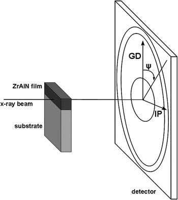
As-deposited and heat-treated samples were analyzed at beamline 1-ID at the Advanced Photon Source at Argonne National Lab using high-energy x-ray radiation with a wave length of λ = 0.1907 Å. The samples were placed with the film in the 10 × 10 μm2 beam with the growth direction (GD) vertical to the beam as schematically shown in Fig. 1. A two-dimensional detector (GE Angio, Billerica, MA) was placed at 1304 mm from the sample for detection of wide angle scattered (WAXS) diffracted intensity. A second two-dimensional detector (PI CCD; Princeton Instruments, Trenton, NJ) was placed at a distance of 4050 mm from the sample to detect the small angle scattering (SAXS). The sample-to-detector distance was calibrated using CeO powder. The WAXS exposures consisted of 10 summed 2-s snap shots and the SAXS exposures were taken for 20 s.
Schematic of the setup during x-ray scattering experiments. The tilt angle, ψ, and the film in-plane (IP) and growth (GD) direction are shown.

The two-dimensional WAXS diffraction patterns were transformed into 5°-wide azimuthal bins resulting in 72 one-dimensional line-outs. A pseudo-Voigt function was fitted to the diffraction peaks for each lineout to extract the plane spacing (d), the integrated intensity, and the integral breadth (Δ2θ).
The general contributions to peak broadening are

where  is the average microstrain and D is the crystallite size. The measured peak broadening is corrected for instrumental contribution where the integral breadth of the substrate peaks is used as a measure of the instrumental broadening. The contributions from size and microstrain to the peak broadening, Δ2θ, are separated by plotting the peak broadening as a function of sin(θ). The ZrN 111, 200, 220, 311, and 222 reflections are used and a linear function is fitted to the data. The two contributions are then separated by use of Eq. (1).
The average macrostrain in the film measured from the 200 reflection in the in-plane (IP), ψ = [80:100°], and GD, ψ = [−10:10°], is determined as  , where d 0 is the unstrained lattice parameter. d 0 was determined at a tilt angle of ψ = 30°, which is the orientation in these coatings where the lattice spacing is invariant as a function of internal strain. The invariant tilt angle is calculated through the Reuss modelReference Almer, Lienert, Peng, Schlauer and Odén25 using single crystal elastic compliances (S 11 = 1.73, S 12 = −0.243, and S 44 = 7.809 1/TPa) determined by ab initio calculations.Reference Brik and Ma26
The SAXS data were corrected for detector dark current and background scattering, e.g., air scattering. Transformation to one-dimensional line-outs at ψ = 45° was performed using 6°-wide azimuthal bins. The line-outs were then fitted to a size distribution function using the maximum entropy methodReference Jemian, Weertman, Long and Spal27 in the IRENA package for IGORReference Ilavsky and Jemian28 assuming spherical particles. The scattering contrast was estimated using the scattering contrast calculator in the IRENA package. The scattering species can be grains of c-ZrN, c-AlN, or h-AlN or amorphous domains with a different chemical composition than that of the matrix, why a mean value for the scattering contrast [(Δρ)2 = 100 × 1020 cm−4] was used. Since the value only changes the calculated volume of scattering particles, it is still possible to make qualitative comparisons of the size distributions. From the size distributions, the number of scattering particles and the mean particle diameter was extracted between 40 and 260 Å, where 40 Å corresponds to the smallest detectable particle size.
III. RESULTS
The composition of the as-deposited film determined by ERDA is Zr0.52Al0.48N1.11. The thickness of the film is 7.5 μm as determined from fractured cross sections studied in the SEM. The appearance of the film is glassy and no columnar structure can be observed (not shown).
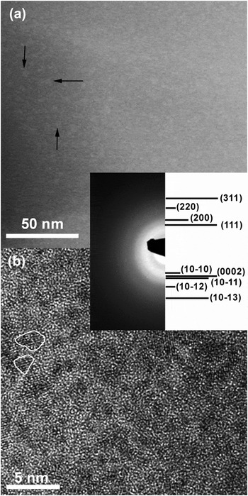
Figure 2(a) shows an elemental contrast scanning transmission electron micrograph (STEM) micrograph from the as-deposited film. Contrast from compositional variations can be seen in the micrograph with ZrN- and AlN-rich features that are 1–2 nm in diameter. Some of the bright contrast AlN-rich features are marked with black arrows in the figure. In the high-resolution transmission electron micrograph (TEM) micrograph, Fig. 2(b), small crystalline grains are observed with a size of the order of 2–5 nm. Between the grains, the structure is amorphous. The corresponding SAED pattern shows broad and diffuse diffraction rings. The diffraction rings can be assigned to a mixture of one cubic and one hexagonal phase.
(a) STEM and (b) high-resolution TEM micrographs with selected area electron diffraction pattern as inset of the as-deposited film. The arrows in (a) point at AlN-rich domains and the white lines in (b) show the outline of two grains.

Figure 3(a) shows an elemental contrast STEM micrograph of the film after annealing at 1250 °C. A stronger contrast is observed and the ZrN- and AlN-rich domains are larger in this case compared to the as-deposited film. In the high-resolution micrograph of the annealed film, Fig. 3(b), a larger part of the film is crystalline and the grains are larger than in the as-deposited case. The diffraction rings in the SAED pattern are better defined in this case and the rings with high intensity belong to a cubic structure. Low intensity diffraction rings from a hexagonal structure can also be observed.
(a) STEM micrograph of the ZrAlN film annealed at 1250 °C; and (b) high-resolution TEM micrograph with selected area electron diffraction pattern inset of the same sample.

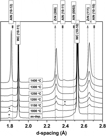
Figure 4 shows one-dimensional WAXS line-outs in the IP direction, ψ = [80:100°], of the as-deposited and annealed films. The diffractogram of the as-deposited film shows no diffraction peaks other than those arising from the substrate. The small peaks centered at d = 1.79 Å and d = 2.40 Å visible in some of the line-outs origin from ZrAl intermetallic macroparticles in the films.29, 30 After annealing at 1150 °C, small diffraction peaks from c-ZrN and h-AlN can be observed. Between 1200 and 1300 °C, the intensity of the c-ZrN diffraction peaks increases, while the peaks from h-AlN remain small. Annealing at 1400 °C causes the c-ZrN peaks to narrow and increase in intensity and also the intensity of peaks from the h-AlN phase increase.
Wide angle scattering line-outs in the film in-plane direction of the as-deposited and annealed films. Peaks labeled with * arises from ZrAl intermetallic macroparticles in the films.

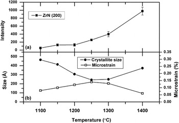
Figure 5(a) shows the integrated IP intensity of the c-ZrN (200) diffraction peak as a function of annealing temperature. The intensity increases slightly for annealing temperatures between 1050 and 1250 °C. After annealing at temperatures higher than 1250 °C, the increase is greater. A similar increase is observed in the film GD (not shown). Figure 5(b) shows the microstrain and crystallite size determined from the broadening of the c-ZrN diffraction peaks. Between 1100 and 1250 °C, the crystallite size decreases, while the microstrain increases. Between 1300 and 1400 °C, the reverse trend is observed.
(a) in-plane intensity and (b) crystallite size and microstrain derived from the c-ZrN 200 peak.

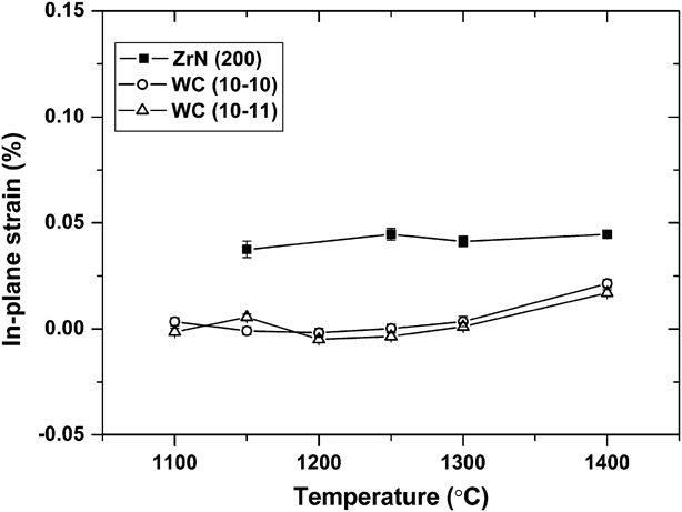
Figure 6 shows the IP macrostrain for c-ZrN and WC phases as a function of temperature. The c-ZrN strain is small, tensile, and does not change significantly with temperature. The strain in the WC substrate is close to zero at all temperatures, with a slight tensile component after the highest temperature anneal.
In-plane strain for the ZrN (200) planes and WC (10-10) and (10-11).
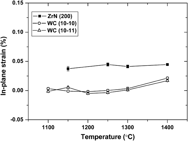
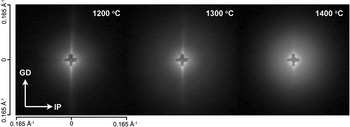
Figure 7 shows the detected SAXS signal for three annealing temperatures. The cross-shaped feature in the middle is the beam stop. Observed are also vertical streaks arising from scattering at the beam-defining slits. With increasing annealing temperature, the intensity of the SAXS pattern increases. After annealing at 1400 °C, the scattered intensity decreases at large angles and becomes higher at small angles due to an increased particle size.
Detected SAXS intensity at three temperature steps. The in-plane (IP) and growth direction (GD) are labeled.

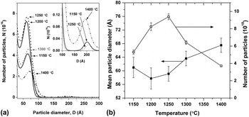
Figures 8(a) and 8(b) show the SAXS-derived particle size distribution and the extracted mean diameter and number of scattering particles, respectively. For annealing temperatures lower than 1150 °C, there is not enough scattered intensity to extract qualitative data. Between 1150 and 1250 °C, the maximum number of scattering particles is found around a diameter of 60 Å. Inserted in Fig. 8(a) is also a zoomed-in part of the size distribution for three temperature steps showing a second peak in the size distribution around a diameter of ∼200 Å. The size of this peak shows no changes with temperature below 1400 °C. For all annealing temperatures, there is also a tail in the size distribution toward higher diameters and smaller peaks centered at ∼320 and ∼430 Å. The number of scattering particles increases with temperature up to 1250 °C as can be seen in Fig. 8(b). At temperatures higher than 1250 °C, the maximum number of scattering particles is shifted to larger diameters. At 1400 °C, the distribution is also wider and the increase of the second small peak around 200 Å at this temperature is attributed to coalescence of smaller particles. In Fig. 8(b), the number of particles is observed to decrease for annealing temperatures above 1250 °C. The particle mean diameter decreases between 1150 and 1200 °C, increases at temperatures higher than 1250 °C, and reaches a maximum value of 67 Å after annealing at 1400 °C.
(a) size distribution and (b) size (filled symbols) and number (open symbols) of scattering particles as a function of temperature. Inserted in (a) is a zoomed-in part around 175 Å of the size distribution.

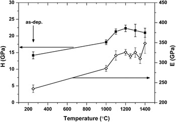
Figure 9 shows the hardness and elastic modulus as a function of annealing temperature. Both the hardness and elastic modulus of the as-deposited film are rather low, compared to ZrN, with H = 14.2 GPa and E = 235 GPa. After annealing, the hardness and elastic modulus increase. The hardness reaches a maximum of 22.4 GPa after annealing in 1250 °C, while the elastic modulus increases to its maximum value of 348 GPa at 1400 °C.
Hardness and elastic modulus as a function of annealing temperature.

IV. DISCUSSION
A. Structure of the as-deposited film
The as-deposited Zr0.52Al0.48N1.11 film has a nanocomposite structure with small grains surrounded by an coalescence or disordered matrix, see Fig. 2(b). As observed from the STEM micrograph, Fig. 2(a), some separation into ZrN- and AlN-rich domains has taken place already during deposition. No previous studies report a solid solution structure for such a high Al content for the ZrAlN system but a mixture of cubic, hexagonal, and/or amorphous regions has been observed.Reference Hasegawa, Kawate and Suzuki20–Reference Rogström, Johnson, Johansson, Ahlgren, Hultman and Odén22 The broad diffraction rings in the SAED pattern, Fig. 2, can be assigned to a two-phase structure with small c-ZrN and h-AlN grains, although the broadness makes the identification difficult. Deposition of two immiscible phases can result in hindered grain growth and causes renucleation during deposition,Reference Petrov, Barna, Hultman and Greene31 which is a strategy used to grow other nanocomposite films, see, e.g., Refs. Reference Diserens, Patscheider and Lévy32–Reference Sandu, Medjani, Sanjinés, Karimi and Lévy34.
In this study, the substrate holder was not rotated during deposition, wherefore the film is under constant ion flux during growth. This will increase the deposition rate and also the local temperature of the film during depositionReference Anders35 compared to depositions with substrate holder rotation but otherwise similar parameters.Reference Rogström, Johnson, Johansson, Ahlgren, Hultman and Odén22 Higher temperature would give the atoms in the growing film more energy for diffusion and thus higher possibility to find low-energy sites. In the present case, however, even smaller grains are observed compared to what was obtained in Ref. Reference Rogström, Johnson, Johansson, Ahlgren, Hultman and Odén22, which could be due to the larger amount of ion bombardment and higher deposition rate. The substrate bias is also lower here compared to earlier studies,Reference Rogström, Johnson, Johansson, Ahlgren, Hultman and Odén22, Reference Rogström, Johnson, Johansson, Ahlgren, Hultman and Odén23 which further limits the atom mobility.
The film has a nitrogen-to-metal ratio above one, which has previously been observed for nanocomposite ZrAlN thin films.Reference Rogström, Johnson, Johansson, Ahlgren, Hultman and Odén22 This is likely a result from limited adatom mobility during growth, which causes formation of vacancies on the metal sublattice as has been observed for ZrN thin films.Reference Yee, Cuomo, Frisch and Smith36, Reference Perry37 The amorphous phase present in the ZrAlN films here might also be able to accommodate a high nitrogen content.
B. Structure evolution during annealing
Further separation into ZrN- and AlN-rich domains has taken place after annealing at 1150 °C, as observed from the WAXS line-outs diffraction experiment in Fig. 4 and at 1250 °C as observed from the STEM micrograph in Fig. 3(a). The domains are larger than in the as-deposited state and the contrast between domains is higher. Differential scanning calorimetry (DSC) results for a similar film in Ref. Reference Rogström, Johnson, Johansson, Ahlgren, Hultman and Odén23 showed an exothermic reaction between the deposition temperature and ∼1050 °C, which based on related TiAlN system was assigned to defect annihilation and crystal recovery.Reference Mayrhofer, Hörling, Karlsson, Mitterer and Hultman12, Reference Knutsson, Johansson, Persson, Hultman and Odén14 Thus, the separation of diffraction peaks from c-ZrN and h-AlN at 1150 °C is assigned to growth and improved crystal quality of grains that may be present already in the as-deposited film.
The contrast in SAXS depends on differences in electron density within the material. These differences can arise due to differences in composition or crystal structure or due to voids or pores in the sample. As no voids are observed by TEM, the SAXS contrast arises from differences in composition and/or atomic arrangement. The contrast in STEM arises from differences in chemical composition and the observed size of the domains may be influenced by the projection of overlapping domains. The particle size as determined from SAXS can thus not be directly compared to the size of ZrN- and AlN-rich domains seen by STEM. The size of ZrN- and AlN-rich domains is, however, similar as seen by STEM, wherefore the SAXS-derived size distribution was used to qualitatively compare with diffraction data from the c-ZrN phase.
From the change of diffraction peak intensity of the c-ZrN phase in Fig. 5(a), two temperature regions during growth of c-ZrN can be discerned. Between 1100 and 1250 °C, only a small change in intensity is observed, while the increase is greater above 1250 °C.
In the first temperature region, between 1100 and 1250 °C, the number of scattering domains increases, see Fig. 8(b). The SAXS results also show a small decrease in mean particle diameter between 1150 and 1200 °C, see Fig. 8(b). This is due to the formation of particles with a smaller diameter that results in a broadening of the particle size distribution toward smaller dimensions, see Fig. 8(a). The crystallite size derived from the diffraction peak broadening [Fig. 5(b)] shows the same trend with decreasing crystallite size between 1100 and 1250 °C. There is a large difference between the mean diameter derived from SAXS and the crystallite size derived from the WAXS data. The mean diameter from the SAXS size distribution is a measure on the most commonly present diameter size in the sample. In the size distribution, it is observed that also particles with larger diameters are present. These particles are fewer but make up a relative large volume of the sample due to their size. The WAXS-derived average size is therefore largely influenced by the presence of these larger grains. Between 1250 and 1400 °C, the intensity of the c-ZrN diffraction peaks increases significantly. The WAXS-derived crystallite size shows that the average size increases between 1300 and 1400 °C, and the SAXS results show that the mean diameter is increased within this temperature interval. After annealing at 1400 °C, the number of larger particles has increased as seen in the insert in Fig. 8(b). The SAXS results further show that the number of scattering particles decreases for temperatures above 1250 °C suggesting that the existing grains coalesce and larger grains grow at the expense of the smaller grains.
The WAXS line-outs in Fig. 4 show that the intensity of h-AlN diffraction peaks remains constant below 1400 °C. Thus, during separation of ZrN and AlN, c-ZrN nucleates and grows in the ZrN-rich domains, while the structure of AlN-rich domains is still partly amorphous with only small h-AlN grains. The slower growth of h-AlN compared to c-ZrN during annealing of ZrAlN thin films was also observed in Refs. Reference Rogström, Johnson, Johansson, Ahlgren, Hultman and Odén22 and Reference Rogström, Johnson, Johansson, Ahlgren, Hultman and Odén23. h-AlN is a stoichiometric compound that can not dissolve nitrogen contents higher than 50 at.%, thus, the high nitrogen content in the film can hinder formation of h-AlN. As observed from DSC/thermogravimetry (TG) results in Ref. Reference Rogström, Johnson, Johansson, Ahlgren, Hultman and Odén23, nitrogen is lost from the film at about the same temperature as the formation of h-AlN. c-ZrNx is less sensitive for the nitrogen concentration and can form even with nitrogen contents higher than x = 1.Reference Dauchot, Edart, Wautelet and Hecq38–Reference Benia, Guemmaz, Schmerber, Mosser and Parlebas40 Further, the c-ZrN phase can dissolve small amounts of Al and form a metastable c-ZrAlN phase.Reference Lamni, Sanjinés, Parlinska-Wojtan, Karimi and Lévy21, Reference Spillmann, Willmott, Morstein and Uggowitzer41, Reference Ruan, Huang, Chen and Lii42 The observed ZrN phase can thus contain both a higher nitrogen content than 50 at.% and possibly some Al.
The macrostrain in the c-ZrN phase is small for all temperatures. The c-ZrN formed can be expected to have a smaller molar volume than the amorphous matrix. A smaller molar volume of the cubic phase would cause tensile strains in this phase, which is also observed. In addition, thermal strains should appear due to difference in coefficient of thermal expansion (CTE) between the substrate, c-ZrN, and the amorphous phase. The CTE of c-ZrN [7.24 × 10⁻⁶ °C−1 (Ref. Reference Toth43)] is higher than that of the substrate [∼5 × 10⁻⁶ °C−1 (Ref. Reference Uhrenius44)]. As the measurements are performed at a temperature lower than the formation temperature of c-ZrN, this would result in tensile stresses. The simultaneous effect of molar volume mismatch and thermal strains makes the two contributions not possible to separate in this case.
The microstrain changes with temperature and increases between 1100 and 1250 °C, connected to the nucleation of new grains as seen by the decreased particle size derived from the SAXS and WAXS data. Compositional fluctuations within the new grains are most likely the largest contribution to the microstrain. Further growth of the grains at temperatures between 1300 and 1400 °C causes the microstrain to decrease as the composition within the grains becomes more homogeneous.
C. Mechanical properties
Nanocomposite films consisting of an amorphous phase and one or more crystalline phases have previously been seen to exhibit very high hardness.Reference Veprek and Reiprich1, Reference Veprek, Niederhofer, Moto, Bolom, Männling, Nesladek, Dollinger and Bergmaier2 In the as-deposited ZrAlN films, however, the hardness is low compared to other nanocomposites. The hardness of arc evaporated ZrN is usually found in the range between 20 and 30 GPa.Reference Gruss, Zheleva, Davis and Watkins45, Reference Niu, Li, Lv, Chen, Feng, Fan, Yang and Yang46 At too small grain sizes, the hardness can decrease as has been observed for CrNReference Mayrhofer, Tischler and Mitterer47 and ZrN.Reference Tung, Huang, Tsai, Ai and Yu48 This has been explained by grain boundary sliding and an increased porosity due to the large amount of grain boundaries.Reference Siegel and Fougere49, Reference Schiotz, Di Tolla and Jacobsen50 In this case, there is a large amount of amorphous or disordered material in the as-deposited film. Thus, in addition to an increased fraction of grain boundaries due to the small grains, the amorphous phase might exhibit a low hardness.
During annealing, the hardness increases and is at all temperatures higher than for the as-deposited film. The maximum hardness is found for the film annealed at 1250 °C. At this temperature, the fraction of c-ZrN grains has increased as observed from the SAXS results, see Fig. 8(b). The mean grain size is, however, not larger than after annealing in 1150 °C. Thus, the maximum hardness is obtained as the film consists of small crystalline grains with a smaller amount of amorphous phase compared to the as-deposited film. For Ti–Si–N films, it has been observed that a maximum hardness is obtained when there is just enough amorphous phase to cover the crystallites.Reference Patscheider, Zehnder and Diserens33 It was found that when the amount of amorphous phase is too large, the lower hardness of this phase caused the hardness of the films to decrease, similar to the as-deposited film here.
Annealing in temperatures higher than 1250 °C causes the hardness to decrease slightly. This is connected to growth of the c-ZrN grains and at 1400 °C with the formation of h-AlN. Similar results were obtained for the mechanical properties as a function of annealing temperature for nanocomposite Ti–Si–C thin films.Reference Rester, Neidhardt, Eklund, Emmerlich, Ljungcrantz, Hultman and Mitterer51 In these Ti–Si–C films, the increased fraction of crystalline TiC increased the hardness, while at higher annealing temperatures, the increased size of TiC grains caused the hardness to decrease.
The elastic modulus of the ZrAlN film increases with annealing temperature and reaches its maximum after annealing in 1400 °C. KimReference Kim and Bush52 showed that the elastic modulus of a nanocrystalline material is dependent on both the grain size and the porosity. The increase can thus be related to both an increased grain size, decreased porosity, and decreased amount of the amorphous phase. This was also observed as the fraction of TiC increased and the amount of amorphous phase decreased in Ti–Si–C films.Reference Rester, Neidhardt, Eklund, Emmerlich, Ljungcrantz, Hultman and Mitterer51 The value for the ZrAlN film is after annealing at 1400 °C 348 GPa, between the values for c-ZrN (460 GPaReference Török, Perry, Chollet and Sproul53, Reference Perry54) and h-AlN (300 GPaReference Gerlich, Dole and Slack55, Reference Mortet, Nesladek, Haenen, Morel, D’Olieslaeger and Vanecek56).
V. CONCLUSIONS
Nanocomposite ZrAlN thin films consisting of nanometer-sized grains of c-ZrN and h-AlN embedded in an amorphous ZrAlN matrix were deposited using cathodic arc evaporation. The hardness of the as-deposited film is low due to the large amount of amorphous phase and the small crystallite size. Annealing of the film causes a phase transformation of the amorphous phase to the equilibrium phases c-ZrN and h-AlN. The transformation can be divided into three steps. First, for annealing temperatures between 1100 and 1250 °C, nucleation of c-ZrN grains is dominating with additional growth of the existing c-ZrN grains. In the second step, between 1250 and 1400 °C, growth of the c-ZrN grains occurs. Finally, growth of h-AlN grains is suppressed until a temperature of 1400 °C, which is assigned to the presence of Zr and a large amount of N in the AlN-rich domains at lower temperatures. The nucleation of c-ZrN improves the mechanical properties of the film, and a maximum hardness is obtained, while there is a minimized amount of amorphous phase in the nanocomposite before h-AlN growth.
ACKNOWLEDGMENTS
The Swedish Research Council (VR) Project and Linnaeus Grants as well as the VINNEX center of Excellence on Functional Nanoscale Materials (FunMat) are acknowledged for the financial support. Dr. Naureen Ghafoor, Linköping University, assisted with TEM work with instruments provided by the KAW Foundation. The use of the Advanced Photon Source was supported by the U.S. Department of Energy, Office of Science, Office of Basic Energy Sciences under Contract No. DE-AC02-06CH11357.