I. INTRODUCTION
With the continuous miniaturization of electronic devices, the solder joints are downsizing and the current density passing through them is increasing. The flip chip solder joints are approaching 50 μm in future. As a result, the average current density will be up to 104 A/cm2 even if a current of 0.2 A is applied. Under such a high current density, electromigration (EM) damage in ultrafine solder joints becomes a critical reliability issue.Reference Tu1 In the past years, several research groups studied the EM behavior of flip chip solder joints and found that EM-induced failure generally occurred in the current crowding region at the cathode due to the formation of pancake-type voids or the excessive consumption of under bump metallizations (UBMs).Reference Zhang, Ou, Huang, Tu, Gee and Nguyen2–Reference Lin, Lai, Lin and Kao7
Electroless Ni–P immersion gold (ENIG) is widely used as a pad finish for ball grid array (BGA) and flip chip packaging. The electroless Ni–P film is an excellent diffusion barrier in lead-free soldering, which can suppress the excessive growth of interfacial intermetallic compounds (IMCs).Reference Strandjord, Popelar and Jauernig8 However, the black pad is a potential reliability concern. To eliminate the black pad issue, the electroless nickel electroless palladium immersion gold (ENEPIG) has been developed as an alternative pad finish. In the ENEPIG system, the immersion Au layer provides oxidation resistance and better wettability between the solder and the pad; the electroless Pd layer improves the wettability and acts as a diffusion barrier as well as the electroless Ni–P layer.Reference Yen, Tsai, Fang, Lo, Hsieh and Lee9
The wetting reactions of lead-free solders on ENEPIG system have been studied. Peng et al.Reference Peng, Wu, Ho and Huang10 investigated the soldering reactions between an Au/Pd/Ni(P) trilayer structure and two solders (Sn–37Pb and Sn–3.0Ag–0.5Cu) and found that the Ni3Sn4 and (Cu,Ni)6Sn5 IMCs are formed at the interfaces, respectively. Yoon et al.Reference Yoon, Noh, Yoon, Kang and Jung11 also investigated the soldering reaction between Sn–3.0Ag–0.5Cu solder and ENEPIG substrate and found that the (Ni,Cu)3Sn4 is formed at the concave sites between the discontinuous (Cu,Ni)6Sn5 IMC with increasing reflow time. Wu et al.Reference Wu, Lin, Huang and Ho12 investigated the influence of Pd thickness on the soldering reaction between Sn–3.0Ag–0.5Cu and Au/Pd(P)/Ni(P) surface finish and found that with increasing Pd(P) thickness, the (Cu,Ni)6Sn5 IMC grew more slowly at the interface, whereas the Ni2SnP/Ni3P bilayer became predominant after the first reflow.
Furthermore, the reliability of solder joints with ENEPIG during EM has attracted much interest. Lu et al.Reference Lu, Tseng, Chang, Huang and Liu13 investigated the EM behavior in the ENIG/Sn/ENIG and ENEPIG/Sn/ENEPIG solder joints under a high current density of 104 A/cm2 at 120 °C and found that EM-induced Ni–P consumption and EM-enhanced diffusion of the interfacial Ni3Sn4 IMC layer could be effectively retarded by introducing an additional electroless Pd layer on the Ni–P layer. However, Kim et al.Reference Kim, Lee, Lee, Pai, Chen and Kuo14 investigated the EM behavior of eutectic Sn–Pb bumps with two substrates (Cu and ENEPIG) and found that EM life of Sn–Pb bumps on Cu pad was longer than that on ENEPIG finish.
It offers a challenge to apply lead-free solders for flip chip packaging due to the higher reflow temperature and the higher Sn content compared with those of Sn–Pb solders, which resulted in severe interfacial reactions with lead-free solders. The EM-induced interfacial reaction and the failure mechanism in lead-free solder/ENEPIG system need further investigation. The effects of EM on the growth behavior of interfacial IMCs and the consumption of ENEPIG finish in the Ni/Sn–3.0Ag–0.5Cu/ENEPIG flip chip packages, as well as the failure mechanism induced by EM, were investigated in the present work. Three-dimensional (3D) finite element simulation on current density and temperature was also carried out using ANSYS simulation software to better understand the current crowding and Joule heating in the flip chip packages.
II. EXPERIMENTAL PROCEDURES
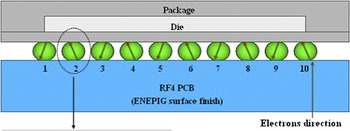
The test vehicles were flip chip packages, each involving a 6 × 6 mm2 silicon chip interconnected to an 18 × 18 × 1.8 mm3 RF-4 printed circuit board (PCB) with 84 BGA solder balls. Figure 1 shows the schematic configuration of the solder joints. The Ni UBM on chip side was 300 μm in diameter and 7 μm in thickness; the underneath Cu trace on chip was 240 μm in width and 25 μm in thickness. The Cu pad on PCB was 250 μm in diameter and 35 μm in thickness; the Cu trace on PCB was 60 μm in width and 35 μm in thickness; the surface finish of Cu pad on PCB was ENEPIG, which consisted of Ni–P, Pd, and Au layers of 5, 0.15, and 0.05 μm in thickness, respectively. The electroless Ni–P contained Ni-15 at.% P.
Schematic of the Ni/Sn–3.0Ag–0.5Cu/ENEPIG solder joint.

The Sn–3.0Ag–0.5Cu (wt%) lead-free solder balls were 300 μm in diameter, and the solder ball pitch was 500 μm. The flip chip test vehicles experienced three reflows, and the height of flip chip solder joints was about 170 μm. As shown in Fig. 2, the single daisy chain which involved 10 solder joints at the edge of the chip was subjected to a constant electric current of 2.45 A, corresponding to a nominal current density of 5 × 10³ A/cm2, defined by dividing the applied current by the area of one Cu pad on PCB. The test vehicles were soaked in silicone oil with a uniform temperature of 140 °C, and the temperature of top surfaces of chips during EM was monitored and controlled at 150 °C. The flip chip packages were also aged at 150 °C for comparison.
Schematic of the daisy chain of flip chip solder joints.

After the experiments, the samples were ground and polished toward the centers of solder joints for cross-sectional examination. The microstructural evolution of the solder joints during EM was examined using a scanning electron microscope (SEM). The compositions of the phases in the solder joints were identified using an electron probe microanalyzer (EPMA).
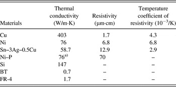
3D finite element simulation on current density and temperature was performed. The model used in this simulation was a SOLID69 eight-node hexahedral coupled-field element. To simplify the thermal and electrical analysis, the simulation model contained only half of the real flip chip test vehicle and the bumps without current stressing were all considered to be cuboids. The entire model utilized a mapped finite element mesh that consisted of 223,755 nodes and 312,102 elements. The average element size in the solder joints was about 7.5 μm. The forced convection boundary condition was applied on all the vehicle surfaces, which exposed to the silicone oil. The material parameters used in the simulation are listed in Table I.
Properties of materials used in the present simulation.Reference Kuan, Liang and Chen15–Reference Siewert, Liu, Smith and Madeni17

a) Referred to the data of Ni.
III. RESULTS
A. Microstructure of as-reflowed Ni/Sn–3.0Ag–0.5Cu/ENEPIG flip chip solder joint
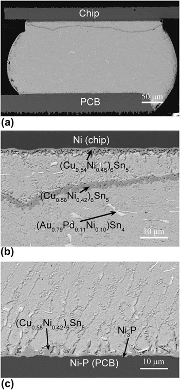
Figures 3(a)–3(c) show the cross-sectional microstructure of an as-reflowed solder joint. As shown in Fig. 3(a), a massive spalling of IMCs occurred in the solder near the solder/Ni UBM interface on chip side and the spalled IMCs were almost a continuous layer. Figure 3(b) shows the higher magnification image of the spalled IMCs and the interfacial IMC layer at the solder/Ni UBM interface. EPMA analysis identified that the interfacial IMC layer contained 30.5 at.% Cu, 25.9 at.% Ni, and 43.2 at.% Sn, i.e., (Cu0.54Ni0.46)6Sn5; the spalled IMCs contained 29.9 at.% Cu, 23.2 at.% Ni, and 46.2 at.% Sn, i.e., (Cu0.58Ni0.42)6Sn5. Kao et al. also observed the massive spalling phenomenon of IMCs and proposed a unified thermodynamic argument.Reference Yang, Ho, Chang and Kao18 They reported that as the content of the reactive constituents in the solder decreased during reaction, the initial intermetallic at the interface became a nonequilibrium phase and the spalling of initial IMCs occurred. In the present work, the initial content of Cu in the bulk solder was 0.5 wt% and the Cu supply was limited during reflow soldering. Therefore, it was believed that the content of Cu in the molten solder gradually decreased with the growth of the Cu–Ni–Sn IMCs at the interface. When the content of Cu decreased to a lower level, the initial (Cu,Ni)6Sn5 IMCs at the interface were not in equilibrium with the molten solder, resulting in the massive spalling of (Cu,Ni)6Sn5 IMCs on chip side. It is noted that the test flip chip solder joints experienced three reflows.
Cross-sectional scanning electron microscope (SEM) images of an as-reflowed solder joint. (a) macrograph of solder joint, (b) at the solder/chip interface, and (c) at the solder/printed circuit board (PCB) interface.

Backscattered electron SEM images show that light color phases precipitated in the whole solder joint, i.e., in the solder matrix and at both of the interfaces. EPMA analyses identified that those light-color phases were (Au,Pd)Sn4 with a solid solution of 1.83 at.% Ni. It was considered that the thin immersion Au and electroless Pd layers in ENEPIG dissolved into the molten solder during reflow, leaving the Ni–P layer exposed to the molten solder. As a result, (Au,Pd)Sn4 phases are formed in the solder and an interfacial IMC layer is formed at the solder/Ni–P interface on PCB side. The interfacial IMC on Ni–P was identified to be (Cu0.58Ni0.42)6Sn5. A thin dark layer, confirmed to be Ni3P, is formed at the (Cu,Ni)6Sn5/Ni–P interface, as shown in Fig. 3(c).
B. Growth behavior of interfacial IMCs and depletion of Ni–P layer during aging
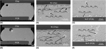
The growth behavior of interfacial IMCs during aging at 150 °C was investigated for comparison with that during EM. Figures 4(a)–4(f) show the cross-sectional microstructure of solder joints after aging for various times. In general, the interfacial IMCs at both of the Ni UBM/Sn–3.0Ag–0.5Cu and Ni–P/Sn–3.0Ag–0.5Cu interfaces grew thicker and became flat with increasing aging time.
Cross-sectional SEM images of the solder joints after aging at 150 °C for (a) 400 and (d) 1000 h, respectively. (b) and (c) higher magnifications of (a). (e) and (f) higher magnifications of (d).

After aging for 400 h, the interfacial IMC at the Ni UBM/solder interface was obviously thicker than that of as-reflowed state, as shown in Fig. 4(b). EPMA analysis identified that the initial (Cu,Ni)6Sn5 IMC at the Ni UBM/solder interface had already transformed into (Ni0.80Cu0.20)3Sn4, whereas the massive spalled IMCs in the solder near the interface remained to be (Cu,Ni)6Sn5, containing 31.7 at.% Cu, 23.9 at.% Ni, and 40.6 at.% Sn. As shown in Fig. 4(c), the interfacial IMC at the Ni–P/Sn–3.0Ag–0.5Cu interface on PCB side was still (Cu0.56Ni0.44)6Sn5 after aging for 400 h. It was clearly shown that after aging for 400 h, the interfacial IMC on the Ni–P remained to be (Cu,Ni)6Sn5, but that on the Ni UBM had transformed from (Cu,Ni)6Sn5 into (Ni,Cu)3Sn4.
After aging for 1000 h, the interfacial IMC layer and the spalled IMCs near the Ni UBM/solder interface were (Ni0.94Cu0.06)3Sn4 and (Cu0.58Ni0.42)6Sn5, respectively, as shown in Fig. 4(e). The interfacial IMC at the Ni–P/solder interface had also transformed into (Ni0.76Cu0.24)3Sn4, as shown in Fig. 4(f).
In the Ni/Sn–3.0Ag–0.5Cu/ENEPIG system, the Cu supply in the Sn–3.0Ag–0.5Cu solder was limited because the diffusion of Cu atoms from Cu pads on chip and on PCB into the solder was inhibited by the Ni UBM and the Ni–P layer, respectively. The Cu content in the Sn–3.0Ag–0.5Cu solder decreased with increasing aging time because the growth of the interfacial (Cu,Ni)6Sn5 IMCs consumed Cu atoms. When the Cu content in the solder decreased to a critical value, the supply of Cu atoms was not enough for the formation of (Cu,Ni)6Sn5 IMCs at the interfaces, resulting in the formation of interfacial (Ni,Cu)3Sn4 IMCs.
Furthermore, compared with the as-reflowed case, the (Au,Pd,Ni)Sn4 phases in the solder coarsened remarkably after aging for 400 and 1000 h, as shown in Figs. 4(a) and 4(d), respectively. The (Au,Pd,Ni)Sn4 phases were distributed not only in the solder but also on the top surfaces of interfacial IMCs at both chip and PCB sides. With increasing aging time, the (Au,Pd,Ni)Sn4 phases coarsened and occupied a larger surface area of interfacial IMCs. The potential effect of (Au,Pd,Ni)Sn4 phases on the mechanical properties of flip chip solder joints is still unclear.
However, the distribution of (Au,Pd,Ni)Sn4 phases was not continuous at the interfaces even after aging for 1000 h. Chang et al.Reference Chang, Ho, Yang and Kao19 reported that a continuous (Au0.4Ni0.6)Sn4 layer could form if the Au content was 0.8 wt%, and a continuous (Au0.4Ni0.6)Sn4 layer could not form if the Au content was 0.4 wt%. The limit was between 0.4 and 0.8 wt%Au. In the present work, the Pd and Au layers in ENEPIG finish were approximately 0.15 and 0.05 μm in thickness, respectively. Assuming that all the Pd and Au layers dissolved into the solder, the calculated contents of Pd and Au in the solder are 0.08 and 0.05 wt%, respectively. Although the contents of Pd and Au in the solder were far less than the limit pointed out by Chang et al.,Reference Chang, Ho, Yang and Kao19 the (Au,Pd,Ni)Sn4 phases were frequently found at the interfaces in the present work.
C. Growth behavior of interfacial IMCs and depletion of Ni–P layer during EM (electrons flowing from PCB to chip)
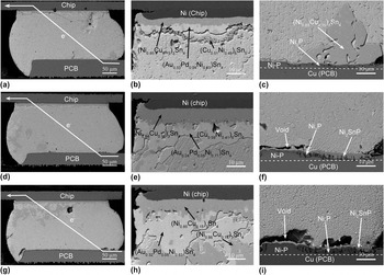
Figures 5(a)–5(i) show the cross-sectional microstructure of the solder joints under a current density of 5 × 10³ A/cm2 at 150 °C for 400, 800, and 1000 h, respectively. The electrons flowed from the PCB to the chip, i.e., the PCB side was the cathode and the chip side was the anode.
Cross-sectional SEM images of the solder joints under 5 × 10³ A/cm2 at 150 °C for (a) 400, (d) 800 h, and (g) 1000 h, respectively. (b) and (c) higher magnifications of (a). (e) and (f) higher magnifications of (d). (h) and (i) higher magnifications of (g). Electrons flowed from PCB to chip.

After EM for 400 h, the Ni–P layer was significantly consumed at the right corner of the cathode interface, leaving a dark Ni3P layer with columnar voids, as shown in Fig. 5(c). Large IMC particles formed at the right corner of the cathode interface and EPMA analysis identified that these IMC particles were (Ni0.85Cu0.15)3Sn4, compared with those of (Cu0.56Ni0.44)6Sn5 after aging for 400 h. It was clear that the dissolved Ni atoms from Ni–P upon electron current stressing induced the transformation of initial interfacial (Cu,Ni)6Sn5 into (Ni,Cu)3Sn4. Furthermore, no (Au,Pd,Ni)Sn4 phases were observed at the cathode interface. The microstructure at the Sn–3.0Ag–0.5Cu/Ni–P interface after EM for 400 h was obviously different from that after aging for 400 h.
After EM for 800 h, there were no interfacial IMCs at the cathode interface, as shown in Figs. 5(d) and 5(f). The interfacial IMCs dissolved in the solder upon electron current stressing. The Ni–P layer at the right corner of the cathode interface was completely consumed and crystallized into Ni3P. A Ni2SnP layer, identified by EPMA analysis, formed at the interface between the solder and Ni3P. There were also voids in the Ni2SnP layer at the cathode interface.
After EM for 1000 h, the Ni–P layer at the cathode interface was almost completely consumed and large voids formed at the cathode interface, as shown in Figs. 5(g) and 5(i). It was concluded that the fast diffusion of Ni atoms away from the cathode upon electron current stressing resulted in the formation of voids. As shown in Fig. 5(i), the Ni–P layer under the left void was not consumed but the Ni–P layer under the right void was completely consumed leaving a Ni3P layer. An appropriate explanation for this phenomenon is as follows. Before the Ni–P layer was consumed, the void at the left side formed at the Ni–P/Sn–3.0Ag–0.5Cu interface. Due to the existence of interfacial void, the diffusion of Ni atoms from Ni–P layer into solder was inhibited. As a result, the Ni–P layer was not consumed. But the void at the right side was not formed at the Ni–P/Sn–3.0Ag–0.5Cu interface before the depletion of Ni–P layer. The diffusion of Ni atoms from Ni–P layer into solder was not inhibited. As a result, the Ni–P layer was consumed and resulted in the formation of Ni3P. However, the Ni2SnP layer at the right corner of the cathode interface after EM for 1000 h was thinner than that after EM for 800 h. This is because that the large voids existed at the interface after EM for 1000 h and Sn could not refill the void region. As a result, only a few Sn atoms reached the interface and reacted with the Ni3P layer to form Ni2SnP.
After EM for 400 h, there was a brighter layer attached to the interfacial IMC on the Ni UBM at the anode interface, as shown in Fig. 5(b). The interfacial IMC was identified to be (Ni0.85Cu0.15)3Sn4, and the brighter layer was identified to be (Au0.33Pd0.04Ni0.63)Sn4. It was shown that the interfacial IMC on the Ni UBM had transformed from initial (Cu,Ni)6Sn5 into (Ni,Cu)3Sn4, and the (Au,Pd,Ni)Sn4 phases tended to deposit at the anode interface during EM. Furthermore, the composition of the spalled IMCs in the solder was (Cu0.51Ni0.49)6Sn5.
After EM for 800 h, the interfacial (Ni,Cu)3Sn4 IMC and (Au,Pd,Ni)Sn4 phases grew remarkably at the anode interface, as shown in Fig. 5(e). After EM for 1000 h, there were large IMCs precipitated at the upper-left corner of the solder joint, as shown in Fig. 5(g). These large IMCs were identified to be (Ni0.86Cu0.14)3Sn4, which attached to the (Au,Pd,Ni)Sn4 phases, as shown in Fig. 5(h). It was considered that the dissolved Ni atoms from the Ni–P layer at the cathode were the main source of Ni atoms. When Ni atoms from the Ni–P were under downwind diffusion, they were driven toward the anode upon electron current stressing and precipitated as large (Ni,Cu)3Sn4 IMCs near the anode interface.
D. Growth behavior of interfacial IMCs and local dissolution of Ni UBM during EM (electrons flowing from chip to PCB)
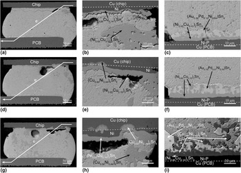
Figures 6(a)–6(i) show the cross-sectional microstructure of the solder joints under a current density of 5 × 10³ A/cm2 at 150 °C for 400, 800, and 1000 h, respectively. The electrons flowed from the chip to the PCB, i.e., the chip side was the cathode and the PCB side was the anode.
Cross-sectional SEM images of the solder joints under 5 × 10³ A/cm2 at 150 °C for (a) 400, (d) 800, and (g) 1000 h, respectively. (b) and (c) higher magnifications of (a). (e) and (f) higher magnifications of (d). (h) and (i) higher magnifications of (g). Electrons flowed from chip to PCB.

After EM for 400 h, the interfacial IMC on the Ni–P of PCB was identified to be (Ni0.85Cu0.15)3Sn4, as shown in Fig. 6(c). There was a brighter layer on the interfacial IMC at the anode interface, which was identified to be (Au0.26Pd0.10Ni0.64)Sn4. It was shown that the interfacial IMC at the Ni–P/Sn–3.0Ag–0.5Cu interface had transformed from initial (Cu,Ni)6Sn5 into (Ni,Cu)3Sn4 after EM for 400 h. The IMC transformation during EM was faster than that during aging. Furthermore, the depletion of Ni–P layer and the formation of Ni3P at the anode interface were minor, which was completely different from that when the Ni–P was the cathode. It was concluded that the flowing direction of electrons played an important role in inducing the consumption of Ni–P layer. The detailed explanation will be given later. With increasing EM time, the interfacial (Ni,Cu)3Sn4 IMC and (Au,Pd,Ni)Sn4 phases grew thicker, while no serious consumption of Ni–P layer occurred.
After EM for 1000 h, the interfacial IMCs on the Ni–P consisted of two IMC layers, i.e., one lower layer of (Ni0.86Cu0.14)3Sn4 on the Ni–P and one upper layer of (Cu0.55Ni0.45)6Sn5, as shown in Fig. 6(i). EPMA analysis identified that the IMC particles in the solder near the anode interface were also (Cu0.55Ni0.45)6Sn5. It was shown that the interfacial IMC at the anode began to transform from (Ni,Cu)3Sn4 into (Cu,Ni)6Sn5 after EM for 1000 h. It was shown that a two-stage transformation of the IMCs at the Ni–P/Sn–3.0Ag–0.5Cu interface (the anode) occurred with increasing EM time. The first transformation from initial (Cu,Ni)6Sn5 into (Ni,Cu)3Sn4 occurred after EM for 400 h, and the second transformation from (Ni,Cu)3Sn4 into (Cu,Ni)6Sn5 occurred after EM for 1000 h. This indicated that the Cu concentration in solder had changed during EM due to the dissolution of Cu pad into the solder upon electron current stressing.
After EM for 400 h, the excessive dissolution of Ni UBM was observed at the right corner of the cathode, as shown in Fig. 6(b). At the Ni/Sn–3.0Ag–0.5Cu interface, besides the continuous IMC layer at the irregular interface, one large IMC particle was also observed in the solder matrix. EPMA analysis identified that the continuous IMC layer at the Ni/Sn–3.0Ag–0.5Cu interface was (Ni0.86Cu0.14)3Sn4 and the IMC particle in the solder matrix was (Ni0.85Cu0.15)3Sn4. It was shown that the interfacial IMC had transformed from initial (Cu,Ni)6Sn5 type into (Ni,Cu)3Sn4 type after EM for 400 h.
After EM for 800 h, voids were observed at the solder/IMC interface at the upper-right corner of the cathode, as shown in Fig. 6(e). EPMA analysis identified that the interfacial IMC was (Ni0.82Cu0.18)3Sn4. However, the Ni UBM in the current crowding region was completely consumed and the local Cu pad was also consumed. The dissolved Ni UBM regions were backfilled with solder and the dissolved Cu pad regions were filled with IMC. EPMA analyses identified that the composition of IMC in the dissolved Cu pad region was (Cu0.95Ni0.05)6Sn5, and a thin Cu3Sn layer was formed at the (Cu,Ni)6Sn5/Cu interface.
After EM for 1000 h, a larger void is formed at the IMC/solder interface, as shown in Fig. 6(h). Localized dissolutions of the Ni UBM and Cu pad were observed at the cathode. Furthermore, EPMA analysis identified that the IMCs in the dissolved regions of Cu pad were (Cu0.67Ni0.33)6Sn5 and those in the solder matrix were (Cu0.56Ni0.44)6Sn5.
It was concluded that once the Ni UBM was completely consumed, the Cu pad began to dissolve in the solder. Due to the high diffusion coefficient of Cu atoms in the solder, the dissolution of Cu pad was significant. The dissolved Cu atoms were driven across the solder to the anode (Ni–P on PCB) upon electron current stressing. One part of the Cu atoms formed a large amount of (Cu,Ni)6Sn5 IMCs in the solder, whereas the other part of the Cu atoms reached the anode interface and changed the interfacial IMC from (Ni,Cu)3Sn4 into (Cu,Ni)6Sn5.
It is interesting to point out that the (Au,Pd,Ni)Sn4 phases always preferred to deposit at the anode interface during EM.
E. Distributions of temperature and current density in flip chip package
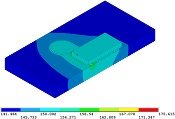
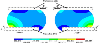
Figure 7 shows the simulated temperature distribution in the flip chip package under a current density of 5 × 10³ A/cm2 at an ambient temperature of 140 °C. The temperature of top surface of the chip ranged from 149.669 to 150.434 °C, which was close to 150 °C measured by the thermocouple. Figure 8 shows the temperature distribution in the two solder joints (joint 4 and joint 7). The hot spots of 163.65 °C are located at the exit of electron flow in the joint 4 and at the entrance of electron flow in the joint 7.
Contour plot for temperature distribution of half flip chip test vehicle (unit: degree celsius).

Cross-sectional contour plot for temperature distribution in the two solder joints (unit: degree celsius).

The minimum temperature in the two joints was 163.17 °C, 23.17 °C higher than the ambient temperature (140 °C), which indicated that serious Joule heating was generated in the solder joints. The temperature difference across the solder joints (4 and 7) was 0.48 °C, corresponding to the temperature gradient of 28 °C/cm. The thermomigration (TM) could be ignored under such a low-temperature gradient.
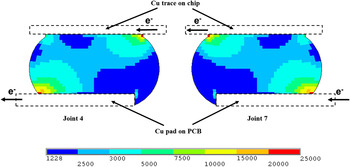
Figure 9 shows the simulated current density distribution in the two solder joints (joint 4 and joint 7). The maximum current density of 2.0 × 10⁴ A/cm2 located at the entrances and the exits of electron flows in the solder joints was four times higher than the average current density of 5.0 × 10³ A/cm2 used in the present work.
Cross-sectional contour plot for current density distribution in the two solder joints (unit: ampere per square centimeter).

IV. DISCUSSION
A. The consumption of Ni–P layer during EM
The consumption of Ni–P during EM strongly depended on the flowing direction of electrons. When electrons flowed from the PCB to the chip, i.e., the Ni–P layer was the cathode, the consumption of Ni–P layer and the formation of Ni3P layer were significantly enhanced. In contrast, when electrons flowed from the chip to the PCB, i.e., the Ni–P layer was the anode, no significant consumption of Ni–P layer occurred. Jang et al.Reference Jang, Kim, Tu, Frear and Thompson20 analyzed the solder reaction-assisted crystallization of electroless Ni–P UBM in the Si/SiO2/Al/Ni–P/63Sn–37Pb multilayer structure and found that the crystallization of electroless Ni–P to Ni3P was induced by the depletion of Ni from electroless Ni–P to form Ni3Sn4. In other words, the depletion of Ni from electroless Ni–P resulted in the consumption of electroless Ni–P layer and the formation of Ni3P layer. Consequently, it was concluded that for the formation of the Ni3P, Ni was the controlling reactive species. The consumption of electroless Ni–P layer is determined by the net flux of Ni atoms diffused out of the Ni–P layer, and the consumption of Ni–P layer during EM could be explained by analyzing the diffusion of Ni atoms.
As mentioned above, the TM effect during EM could be ignored. Thus, only the chemical potential gradient force and the electron wind force were concerned in the consumption of Ni–P layer during EM. Under the chemical potential gradient force, the atomic diffusion flux can be written as follows:

Under electron wind force, the atomic diffusion flux can be written as follows:

where J chem is the diffusion term due to the chemical potential gradient, J em is the diffusion term due to the electron momentum transfer effect, C is the concentration, D is the diffusivity, k is Boltzmann’s constant, T is the temperature, Z* is the effective charge number, e is the electron charge, ρ is the resistance, and j is the current density.
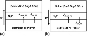
When electrons flowed from the PCB to the chip, i.e., the Ni atoms of Ni–P layer were under downwind diffusion, the flux of Ni atoms induced by the chemical potential gradient force was in the same direction with that induced by the electron wind force, as shown in Fig. 10(a). Thus the total flux of Ni atoms at the Ni–P/solder interface in the flowing direction of electrons was as follows:

Schematic of the flux of Ni atoms at Ni–P/solder interface during electromigration (EM). (a) Ni–P was the cathode and (b) Ni–P was the anode.

On the other hand, when the electrons flowed from the chip to the PCB, i.e., the Ni atoms of Ni–P layer were under upwind diffusion, the flux of Ni atoms induced by the chemical potential gradient force was in the opposite direction with that induced by the electron wind force, as shown in Fig. 10(b). Thus the total flux of Ni atoms at the Ni–P/solder interface in the flowing direction of electrons was as follows:

It was obvious that J 1 is larger than J 2, i.e., the total flux of Ni atoms flowing out of the electroless Ni–P when electrons flowed from PCB to chip was larger than that when electrons flowed from chip to PCB. It is obvious that when Ni–P layer was used as the cathode, the consumption of electroless Ni–P on PCB was significantly accelerated than that when Ni–P layer was used as the anode.
B. The formation of Ni2SnP layer during EM
As mentioned above, when the Ni–P layer was the cathode, the Ni atoms of the Ni–P layer were driven away from the cathode not only by the chemical potential gradient force but also by the electron wind force. As a result, the diffusion of Ni atoms from the Ni–P layer into the solder would be accelerated during EM. As the Ni atoms diffused out of the Ni–P layer, the P atoms remained and accumulated in the original Ni–P layer, forming a Ni3P layer.
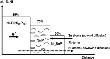
As shown in Fig. 11, the Sn atoms would diffuse from the solder in the opposite direction with that of Ni atoms during EM. Actually, not only Ni3P but also Ni2SnP formed at the Ni–P/solder interface. When the Sn atoms reached the Ni3P/solder interface, Sn reacted with the Ni3P layer to form a Ni2SnP layer between the Ni3P and solder. The interfacial reaction between the Ni3P and Sn is expressed as follows:

Schematic of the formation of Ni2SnP during EM when Ni–P was the cathode.

If the Ni–P had not been completely consumed yet, Ni atoms would diffuse from the Ni–P to the solder leaving the Ni3P layer, and the interfacial reaction is expressed as follows:

Since Ni atoms were under downwind diffusion of electrons, EM enhanced the diffusion of Ni atoms from the Ni–P across the Ni3P and Ni2SnP to the solder. According to the reaction Eq. (5), the massive Ni atoms passing through the Ni2SnP would prevent the reaction from forming Ni2SnP. As a result, the growth kinetic of Ni2SnP was low when the Ni–P layer still existed; once the Ni–P layer was completely consumed, no Ni atoms were passing through the Ni2SnP, and thus the growth kinetic of Ni2SnP was accelerated.
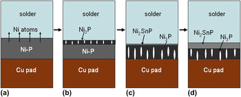
The experimental results in the present work were in good agreement with the above discussion. As shown in Fig. 5(c), at the right corner of the cathode interface, the Ni–P layer was not completely consumed after EM for 400 h and large (Ni,Cu)3Sn4 particles formed at the interface. As a result, the Ni2SnP formed underneath the (Ni,Cu)3Sn4 IMC was very thin. However, as shown in Fig. 5(f), the Ni–P layer was completely consumed and transformed into Ni3P after EM for 800 h, and a thick Ni2SnP layer is formed close to the Ni3P. Additionally, once the Ni–P layer was completely consumed, no extra Ni atoms reacted with Sn atoms to form the interfacial (Ni,Cu)3Sn4, which also dissolved into the solder upon electron current stressing. As a result, without the barrier of interfacial (Ni,Cu)3Sn4 layer, the reaction between Ni3P and Sn was enhanced. Figures 12(a)–12(d) schematically show the Ni–P consumption at the cathode interface.
Schematic of microstructural evolution of Ni–P layer (the cathode) during EM. (a) Ni atoms diffused from Ni–P layer into the solder, (b) Ni3P layer with columnar voids formed at the Ni–P/solder interface, (c) Ni2SnP was thin till the Ni–P layer was completely consumed, and (d) hereafter, the growth of Ni2SnP was accelerated.

V. CONCLUSIONS
The (Cu,Ni)6Sn5 IMCs formed at both interfaces of as-reflowed Ni/Sn–3.0Ag–0.5Cu/ENEPIG solder joints, and the massive spalling of (Cu,Ni)6Sn5 IMCs occurred at the solder/Ni interface. During aging at 150 °C, the transformation of interfacial IMC from initial (Cu,Ni)6Sn5 into (Ni,Cu)3Sn4 occurred after 400 h at the Ni/solder interface while this transformation occurred after 1000 h at the Ni–P/solder interface.
When electrons flowed from the ENEPIG to the Ni UBM at the cathode (ENEPIG), EM significantly enhanced the consumption of Ni–P layer, leaving a Ni3P layer with columnar voids. Once the Ni–P layer was completely consumed, the growth of Ni2SnP was accelerated, which was explained by a proposed model. The dissolved Ni atoms from the Ni–P and the interfacial IMCs were driven toward the anode upon electron current stressing and precipitated as large (Ni,Cu)3Sn4 IMCs. At the anode (Ni UBM), the transformation of interfacial IMC from initial (Cu,Ni)6Sn5 to (Ni,Cu)3Sn4 occurred after EM for 400 h. The excessive consumption of Ni–P and the formation of voids at the cathode were responsible for the EM-induced failures.
When electrons flowed from the Ni UBM to the ENEPIG at the cathode (Ni UBM), the current crowding induced the rapid localized dissolutions of Ni UBM and then Cu pad on chip, resulting in a two-stage transformation of interfacial IMCs at the opposite Ni–P/solder interface. In the first stage, the initial interfacial (Cu,Ni)6Sn5 transformed into (Ni,Cu)3Sn4 after EM for 400 h; in the second stage, the dissolved Cu atoms from Cu pad on chip diffused across the solder to the opposite interface, resulting in the transformation of (Ni,Cu)3Sn4 into (Cu,Ni)6Sn5 after EM for 1000 h. At the anode (ENEPIG), no obvious consumption of Ni–P layer occurred since the diffusion of Ni atoms from Ni–P was retarded under upwind electron flow. The localized dissolutions of Ni UBM and Cu pad, as well as the formation of voids, at the cathode were responsible for the EM-induced failures.
ACKNOWLEDGMENTS
This work is supported by the programs of National Natural Science Foundation of China (Nos. U0734006 and 51171036) and the programs in Liaoning Province (Nos. 2009921058 and 20082163). The design and fabrication of the flip chip packages were supported by Huawei.