Introduction
Beam steering is a method that minimizes interference for neighboring users by precisely focusing the radiated signal and determining the most efficient data-delivery path to a particular receiver. This is accomplished through directivity control of the radiation pattern of the main lobe as shown in Fig. 1 by implementing either digital [Reference Imanishi and Nosaka1] or analog [Reference Qiu and Zhu2] phase shifters to adjust the phases of the radio frequency (RF) signals driving the radiating antennas. The application of beam steering has been limited to specific areas, like radar systems, due to its high cost [Reference Karimkashi, Zhang, Kelley, Meier, Palmer, Zahrai, Doviak and Zrnic3]. However, this approach has recently garnered significant interest for 5G and beyond communication technologies [Reference Baskent, Wang, Lemme and Negra4], in addition to numerous other digital and analog applications, such as smart surfaces [Reference Yan, Yuan and Kuai5].
Conceptual block diagram of beam steering using analog phase shifters.

Analog phase shifters are preferred for RF applications due to their low complexity, cost-efficiency, and wide phase tuning range [Reference Saeed, Hamed, Baskent, Uzlu, Wang and Negra6]. Furthermore, analog phase shifters offer continuous coverage of radiation angle for beam steering, unlike their digital counterparts. Achieving such continuous phase control in analog phase shifters mainly requires a tunable component. Therefore, nonlinear elements such as transistors or varactors are employed.
Among two-dimensional (2D) materials, graphene stands out for RF [Reference Saeed, Hamed, Palacios, Uzlu, Wang, Baskent and Negra7], millimetre- [Reference Saeed, Hamed, Baskent, Uzlu, Wang and Negra8], and submillimetre-wave circuit applications due to its prevailing electrical and mechanical characteristics [Reference Novoselov, Geim, Morozov, Jiang, Zhang, Dubonos, Grigorieva and Firsov9]. However, the zero energy-bandgap of graphene leads to poor switching properties, restricting the utilization of graphene field-effect-transistors (GFETs) in digital circuits [Reference Saeed, Palacios, Wei, Baskent, Fan, Uzlu, Wang, Hemmetter, Wang, Neumaier, Lemme and Negra10]. On the other hand, the linear energy dispersion in the band structure enables the application of graphene in analog circuits. Moreover, the large-scale integrability of single-layer CVD-grown graphene makes it a perfect 2D-material alternative to conventional technologies as well as an add-on [Reference Lemme, Akinwande, Huyghebaert and Stampfer11]. Graphene’s exceptional suitability for varactor design [Reference Baskent, Wang, Lemme and Negra12] stems from its voltage-dependent quantum capacitance, CQ. Moreover, CQ exhibits substantial capacitance adjustment capabilities, particularly when operating at higher frequencies. This unique feature imparts nonlinearity, thereby enhancing its role in enabling phase adjustments.
Various graphene-enabled phase-shifters have been published in the literature using GFETs [Reference Medina-Rull, Pasadas, Marin, Toral-Lopez, Cuesta, Godoy, Jimélnez and Ruiz13, Reference Li, Mao, Gu, Xie, Geng and Chen14], graphene flakes [Reference Yasir, Peinetti and Savi15, Reference Chen, Liu, Ju and Lu16], and graphene diodes [Reference Saeed, Hamed, Baskent, Uzlu, Wang and Negra6]. The GFET phase shifter in [Reference Medina-Rull, Pasadas, Marin, Toral-Lopez, Cuesta, Godoy, Jimélnez and Ruiz13] has encountered limitations related to its cutoff frequency and maximum oscillation frequency. Studies in [Reference Yasir, Peinetti and Savi15, Reference Chen, Liu, Ju and Lu16] have focused on manipulating the resistance of graphene flakes for phase control, but they lack the reproducibility crucial for these applications. Meanwhile, in [Reference Li, Mao, Gu, Xie, Geng and Chen14], the phase control has faced challenges due to current saturation issues, leading to unavoidable fluctuations in insertion loss for an acceptable phase shift.
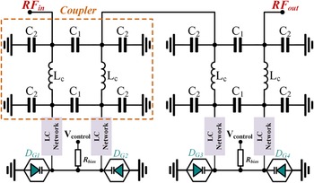
Considering the benefits of graphene, and analog phase shifters, this study introduces a low-cost cascaded millimetre-wave reflective-type phase-shifter (RTPS) designed for 5G and beyond applications as shown in Fig. 2. It leverages thin-film graphene diodes to achieve its objectives. Compared to previous work [Reference Baskent, Wang, Lemme and Negra4] presented at the EuMIC 2024, this study provides a detailed graphene-based diode performance validation, confirming the stability and repeatabilityof the proposed technology. Furthermore, an RF small-signal model is introduced for precise design and performance evaluation. Key enhancements include an investigation of the linearity performance of RTPS through the large-signal measurements.
Schematic overview of the proposed reflective-type phase-shifter.

Thin-film MMIC technology
A thin-film back-end-of-line MMIC technology has been further developed, building upon our previous work, to support the integration of graphene-based diodes alongside high-quality passive components. The cross-section of the developed process used in this work is shown in Fig. 3. In previous technologies, the thin-film-resistor (TFR) layer is prepared before a second dielectric (D2) is processed, which hinders the preservation of graphene quality essential for the performance and reliability of the devices [Reference Saeed, Hamed, Wang, Shaygan, Neumaier and Negra17]. Moreover, the substrate is relatively thick and rigid which prevents the circuits to be applied in flexible applications. The materials of each layer, their thicknesses, and properties are summarized in Table 1.
Cross-sectional overview of the graphene-based thin-film MMIC technology (not to scale).

Thin-film MMIC substrate definition

M1 is used as an anode electrode for the metal-insulator-graphene (MIG) diode, metal plate for capacitors, and bottom connection for inductors. D1 serves as the barrier layer for the MIG diode. M2 is implemented to be a graphene contact metal. D2 is deposited for MIG diode encapsulation, dielectric region for capacitors, and as a separator for inductors. V1 and V2 are the vias through the oxides D1 and D2, respectively. M3.1 is the TFR layer. Finally, M3 defines the second plate of capacitors, interconnections, contact pads, and the spiral structure for inductors.
Metal-insulator-graphene diode
The prototype fabrication was realized on an 8-µ m-thick flexible polyimide (PI) substrate utilizing contact photolithography. Initially, 200-nm deep trenches were etched into the substrate via reactive ion etching (RIE). Then 200 nm of Al and Ti stacks were deposited to fill the trenches via e-beam evaporation and the unwanted metals were lifted off. Subsequently, 6-nm-thick TiO2 was deposited onto the embedded metal electrodes by atomic layer deposition (ALD) using TiCl4 as a precursor and enhanced by oxygen plasma. CVD-grown graphene with a supporting PMMA layer was transferred onto the sample. By using oxygen plasma, the single-layer graphene was patterned to its final shape after the removal of PMMA. Afterward, 50 nm Ni was sputtered to establish an ohmic contact. The process was followed by 80 nm Al2O3 deposition using the ALD at 150 ∘ C to encapsulate the structures beneath. In order to access the metal contacts, vias were etched through the oxide layers by fluorine-based RIE. Then, a 15-nm-thick layer of NiCr was sputtered. Finally, 20-nm Ti and 2-µm Al were deposited, respectively, onto the samples via e-beam evaporation. The microscope image of the fabricated MIG diode is shown in Fig. 4.
DC measurements of the fabricated graphene diode, inset presents the fabricated MIG diode.

DC characterization
Various MIG diode test structures with different sizes and numbers of fingers have been implemented and characterized to find a suitable configuration for the targeted application. The DC characteristics of the representative diode are presented in Fig. 4. Based on the measurements, a two-finger graphene diode, with each finger having dimensions of 80 µ m × 3 µ m is chosen for phase-shifting.
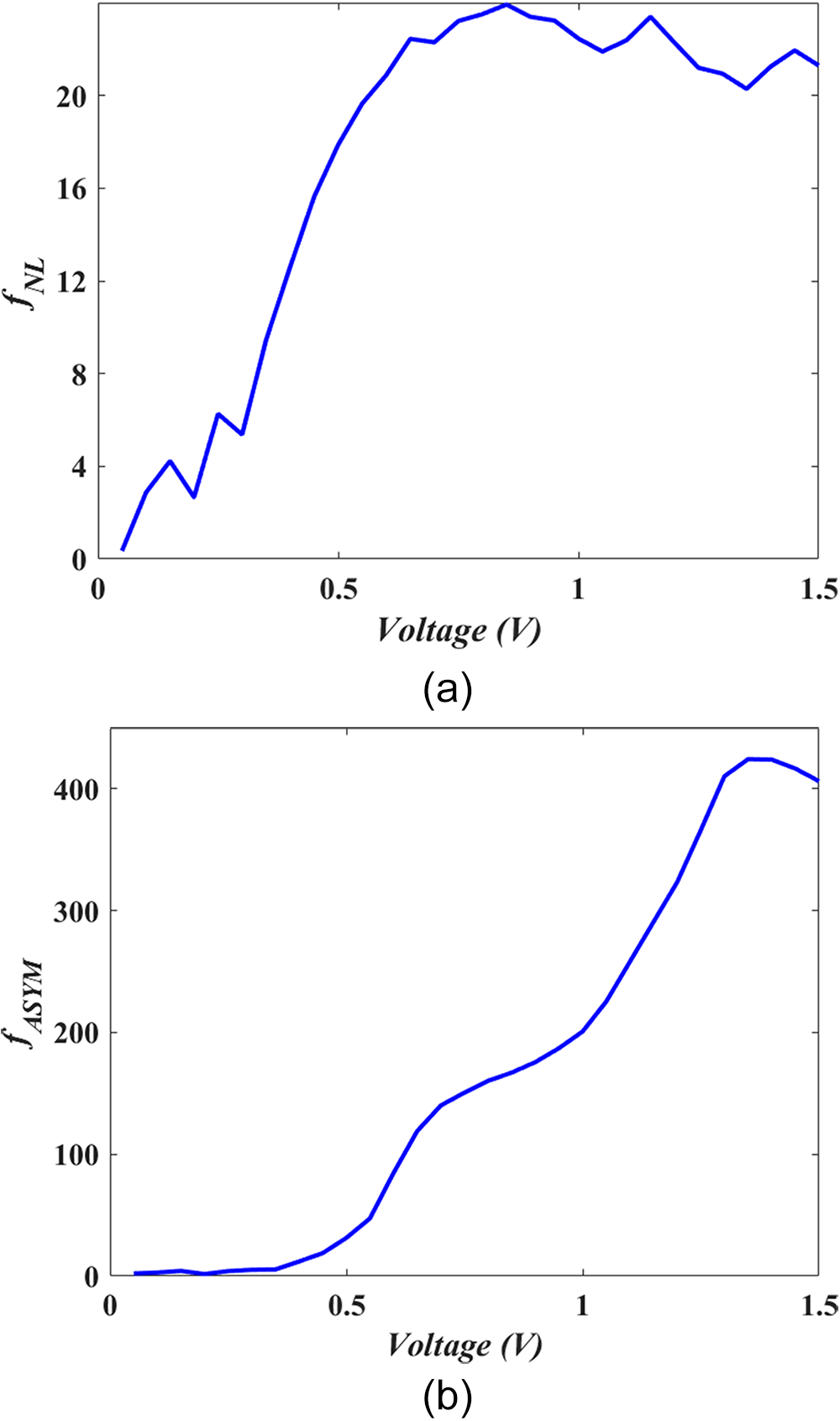
The diode nonlinearity and asymmetry are significant figures-of-merit (FOMs) to evaluate the phase-shifting capabilities of a diode in this configuration. The nonlinearity and asymmetry are calculated from the measured I-V characteristics according to [Reference Periasamy, Berry, Dameron, Bergeson, Ginley, O’Hayre and Parilla18]:
 \begin{equation}
f_{NL} = \frac{dI_{D}/dV_{D}}{I_{D}/V_{D}}
\end{equation}
and
 \begin{equation}
f_{ASYM} = \bigg| \frac{I_{ON}}{I_{OFF}} \bigg| ,
\end{equation}
where ION is the forward current and IOFF is the reverse current, and fASYM represents the current asymmetry of the diode between the ON and OFF states. fNL measures the deviation from a linear resistor which is quantified as the ratio of the differential diode conductance, with respect to the linear resistor conductance [Reference Saeed, Hamed, Baskent, Uzlu, Wang and Negra6].
DC characteristics of this diode exhibit high nonlinearity and asymmetry as shown in Fig. 5a and 5b. Only positive voltages were considered for the fNL since the graphene-based diode shows significant nonlinearity primarily under forward bias due to the Schottky-like behavior at the metal–graphene interface [Reference Urcuyo, Duong, Jeong, Burghard and Kern19]. The nonlinearity for the fabricated diodes is calculated to be above 20. Furthermore, the I-V characteristics of the measured diode reveal an asymmetry above 400.
Key performance metrics of a MIG diode include: (a) nonlinearity and (b) asymmetry as a function of applied bias voltage.

AC characterization
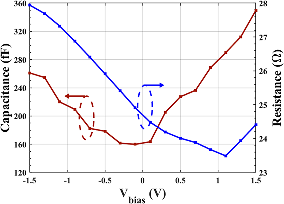
S-parameter measurements for the diode are carried out with a network analyzer and on-wafer Cascade GSG-100 probes. The signal is applied to port P1, the metal electrode of the diode, from 10 MHz to 50 GHz at bias voltages from –1.5 V to 1.5 V. The overall diode capacitance, Ceq, as presented in Fig. 6 is extracted from the measurements in addition to the diode resistance.
S-parameter analysis of MIG diode for the voltage-dependant Ceq at different bias voltages.

Capacitance tuning ratio, tv, is a vital FOM for phase shifters which is identified as the ratio between the maximum and minimum varactor capacitance,  $C_{max}/C_{min}$. The ratio determines the phase-tuning capability of a diode. As illustrated in Fig. 7, the Cmax and Cmin values are measured to be 352 fF and 156 fF, respectively. The tv value is derived from the measured varactor capacitance at f = 30 GHz, exceeding 2.2, and thus outperforms conventional CMOS varactors [Reference Ho, Kuo, Chan, Lien and Guo20, Reference Askari, Kaabi and Kavian21].
Extracted capacitance and resistance at 30 GHz as a function of bias voltage from the fabricated graphene diode.

Diode small-signal-model
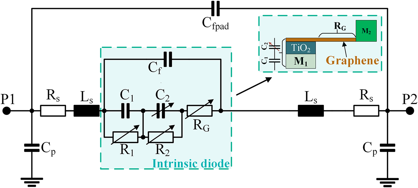
Figure 4 displays the chip micrograph of the fabricated MIG diode on flexible PI substrate in the inset. The cross-sectional view of the intrinsic diode is illustrated in Fig. 8. The diode consists of a parallel plate capacitor formed between M1 and the graphene sheet. Owing to the low density of states in graphene, the diode is represented by two capacitances in series [Reference Luryi22].
Small-signal model of the diode together with a cross-section diagram showing the intrinsic model components.

The intrinsic diode can therefore be modeled as a series combination of a linear capacitance, C 1, and a bias-dependent, nonlinear capacitance, C 2. As a result, the DC bias-dependent nonlinear junction resistance is made up of the series combination of the leakage resistances of the two capacitors, R 1 and R 2, along with the graphene sheet resistance, RG. This series arrangement of C 1, C 2, and RG is in parallel with the fringing capacitance, Cf, located in between the two metal electrodes. Figure 8 illustrates the complete small-signal model including the parasitics from the probing pads. Design considerations are applied to minimize the parallel fringing capacitance, Cf, by embedding the first electrode (M1) into the substrate. Moreover, the physical design ensures that the linear series capacitance, C 1, is larger than the nonlinear capacitance, C 2, making C 2 the dominant factor in the equivalent capacitance.
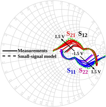
The on-chip S-parameter measurement results obtained are used to determine the values of the lumped elements representing the small-signal model. Figure 9 shows a comparison between the extracted model and the measurement results over the whole 0.01–70 GHz band with less than 1 dB magnitude mismatch and better than 3∘ phase mismatch for the return and insertion loss.
S-parameter simulation of the extracted small-signal model in comparison with the measurement results of the MIG diode at different bias voltages.

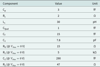
The values of the lumped components for the small-signal equivalent circuit are provided in Table 2. These values align with the physical design considerations. The extracted linear capacitance, C 1, is approximately twenty-seven times larger than C 2, while Cf is around twenty-times less than C 2. At frequencies above 150 MHz, R 1 is effectively shorted by the impedance of C 1, resulting in lower loss at higher frequencies.
Extracted lumped components values in the equivalent circuit

Circuit design and realization
Reflective analog phase shifters are composed of two main parts, namely the coupler and the reflective loads. The coupler divides the RF input signal into two equal amplitude signals with a 90∘ phase difference. These split signals are then reflected and phase-shifted at the load. The coupler combines the reflected signals constructively at the output port. At the input, the reflected signals are 180∘ out of phase, leading to their cancellation and thus to a good input return loss.
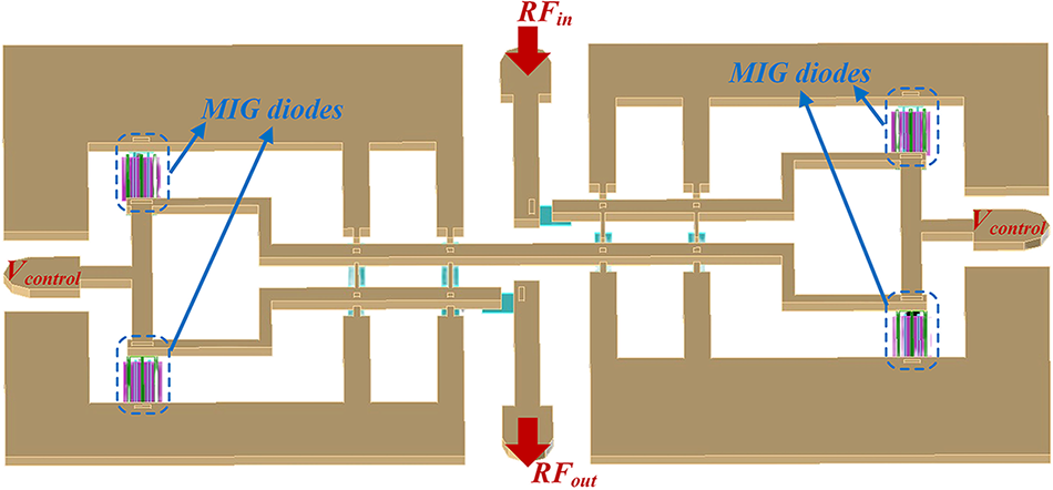
In order to enhance the insertion phase of the conventional RTPS, a cascaded configuration is proposed. The layout of the developed graphene-enabled phase shifter is presented in Fig. 10. The configuration exploits two hybrid branchline couplers to ensure the isolation of the loads from the input and output ports, and four graphene diodes to vary the insertion phase.
Proposed cascaded analog phase shifter.

In order to implement a compact phase shifter, microstrip lines are replaced by lumped elements at the center frequency. The values of the coupler inductance, Lc, and capacitances, C 1 and C 2, are calculated according to [Reference Ellinger, Vogt and Bachtold23]:
 \begin{equation}
L_{c} = \frac{Z_{0}}{2\pi f_{0}\sqrt{2}}
\end{equation}
 \begin{equation}
C_{1} = \frac{1}{2\pi f_{0}Z_{0}}
\end{equation}
 \begin{equation}
C_{2} = \frac{1}{(2\pi f_{0})^2L_{c}} - C_{1}.
\end{equation}
For a characteristic impedance Z0  $= 50~\Omega$ and a center frequency of 30 GHz, the inductance, Lc, is calculated to be 185 pH, the capacitances, C 1 and C 2, are 105 fF and 45 fF, respectively. To achieve the desired minimum insertion loss and a 90∘-phase difference at the outputs, these values are tuned while considering the impact of parasitic elements.
Various RTPS configurations have been studied with different reflective loads in literature. Resistive elements in the load are to be avoided to minimize insertion loss [Reference Ellinger, Mayer, Wickert, Joram, Wagner, Eickhoff, Santamaria, Scheytt and Kraemer24]. In this design single-varactor reflective loads are used to obtain a compact and thus cost-effective RTPS. The loads are supported with a simple LC transformation network to decrease the loss variations within the operation band. The chip micrograph of the fabricated RTPS is shown in Fig. 11.
Chip micrograph of the fabricated cascaded RTPS prototype.

Measurement results
The prototype, occupying less than 0.7 mm2 of chip space, is characterized in both small- and large-signal conditions to confirm its phase-shifting performance as well as power handling capabilities. S-parameter measurements are done across the frequency band from 10 MHz to 50 GHz while the bias voltages were varied from −1.5 V to 1.5 V. The linearity measurements are carried out at the center frequency of 30 GHz with the input power levels and the voltages sweeping from −20 dBm to 5 dBm, and −1.5 V to 1.5 V, respectively.
S-parameters
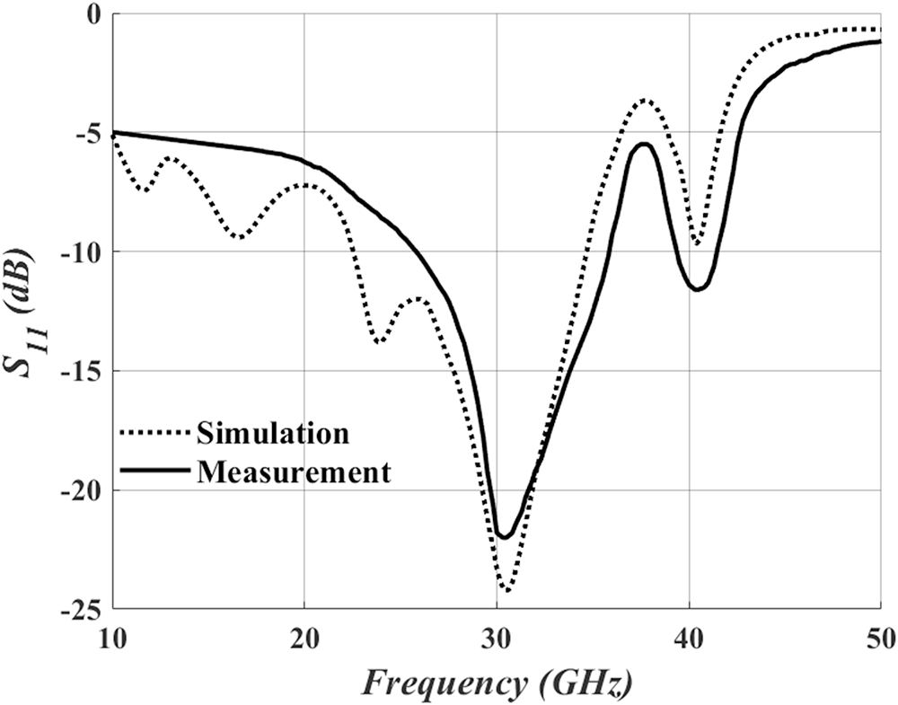
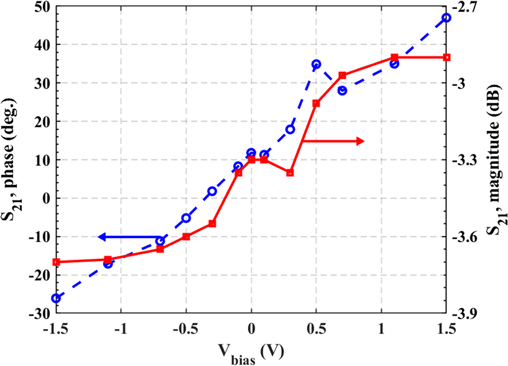
Figure 12 illustrates the comparison between simulated and measured S 11 throughout the target frequency range. The results show good agreement with simulations within the 28–36 GHz band, with better than −13 dB return loss. The magnitude of the measured S 21 is depicted in Fig. 13 and the phase in Fig. 14. Within the intended frequency band, measured S 21 is −3.3 dB ±0.5 dB, aligning well with the anticipated outcomes from simulations. Additionally, the measured phase difference,  $\Delta\phi$, is 75∘ , indicating effective phase-shifting performance with stable and predictable behavior across the frequency range. Figure 15 further presents the phase shift performance at 30 GHz as a function of bias voltage, in terms of both phase and magnitude, demonstrating the device’s tuning capability and linear response.
Measurement and simulation comparison for S 11.

Magnitude of measured insertion loss, S 21.

Phase of the measured insertion loss, S 21.

Phase and magnitude of measured S 21 at 30 GHz.

Linearity characterization
The power handling capability of the analog phase shifter is assessed through the large-signal characterization. The schematic overview of a measurement setup is given in Fig. 16. Two tones at different frequencies, f 1 and f 2, are generated by the signal generator. These signals are combined with a power combiner and fed to the device under test. The bias voltages are applied by an external DC supply. The output power levels are measured by a spectrum analyzer.
Block diagram of the two-tone measurement test setup for the phase shifter.

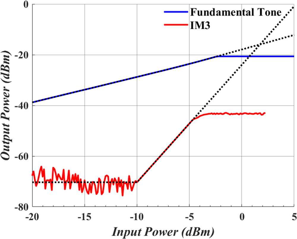
The two-tone measurement test has been carried out to characterize the compression ( $P_{1dB}$) and third-order intermodulation point (IIP3) of the RTPS. Two tones with the frequencies
 $f_{1} = 29.995$ GHz and
 $f_{2} = 30.005$ GHz have been chosen with a spacing of 10 MHz. Figure 17 displays the large-signal performance of the implemented prototype. Here, it can be observed that a 1-dB compression point at the input power of
 $P_{1dB} = -1.5$ dBm and an IIP3 of around −6 dBm is obtained. These values are very high considering a maximum supply voltage of 1.5 V and the chosen cascaded architecture.
Linearity characterization of RTPS.

Table 3 provides a summary of the comparison among cutting-edge graphene-based phase shifters. The proposed circuit in this work uses the largest number of active devices and is designed for the highest frequency band. Additionally, it maintains a constant and minimal insertion loss profile across its operational frequency, distinguishing it from the other fabricated phase shifters. This prototype requires lower control voltages to achieve a high measured phase tuning range. Despite the potential for conventional technologies to provide a greater phase-shifting range within a similar operation band, the most significant advantage of this technology lies in its ability to achieve large-scale integration on any substrate, particularly flexible ones. This feature is essential for a cost-effective implementation of, e.g., mmWave and sub-THz intelligent reflective surfaces.
Comparison with published graphene-based phase shifters

‡ : Simulation results.
Conclusion
The presented circuit, utilizing diodes based on CVD-grown graphene alongside the resilient technology introduced here, stands as a pivotal facilitator in achieving low-cost flexible beam steering on a wide variety of substrates. Thanks to the high-quality graphene, substantial capacitance adjustment capabilities and therefore, a large phase tuning range is achieved. These results pave the way for applications in intelligent surfaces used for 5G and beyond communication, as well as biomedical applications based on 2D materials.
Acknowledgements
This work was financially supported by the European Commission under the projects GrapheneCore3 (contract no. 881603) and WiPLASH (contract no. 863337), and by the German Science Foundation (DFG) under the project GLECS2 (contract no. NE 1633/3-2).
Competing interests
The authors declare no conflict of interest.

Eyyub Baskent received his B.Sc. degree in Electrical and Electronics Engineering from Bilkent University in 2018 and received his M.Sc. degree in Electrical Engineering and Information Technology from RWTH Aachen University, specializing in micro- and nanoelectronics in 2021. Currently, he is a Ph.D. candidate with the Chair of High Frequency Electronics, RWTH Aachen University. His current research interests include the design, development, and characterization of high-frequency electronics circuits based on 2D materials, for communication and biomedical applications.

Zhenxing Wang is the Head of the Graphene Electronics Group, AMO GmbH. He received his Ph.D. degree from Peking University, China, in 2012, on the topic of carbon-nanotube- and graphene-based radio-frequency electronics. After that he joined the University of Erlangen-Nuremberg as a Postdoctoral Researcher, working on solution-based 2D-materials-based nanodevices. Since 2014, he has been with AMO, where he is responsible for the development of graphene-based electronics, especially for high-frequency applications. He is leading different German national projects as well as EU international projects.

Max C. Lemme has been a Full Professor at RWTH Aachen University and Scientific Director of AMO GmbH since 2017. After his Ph.D. degree in Electrical Engineering from RWTH in 2004, he received the “NanoFutur” award from the German BMBF (2006). In 2008, he joined Harvard University with a Humboldt Fellowship to work on graphene devices. He became a Professor at KTH Royal Institute of Technology, Sweden, in 2010. He received an ERC Starting Grant and became a DFG Heisenberg Professor at the University of Siegen in 2012. His research includes electronic devices and semiconductor technology like FinFETs, high-k dielectrics, 2D materials, and, recently, neuromorphic computing.

Renato Negra received his M.Sc. degree in Telematics from TU Graz and his Ph.D. degree in Electrical Engineering from ETH Zurich. From 1998 to 2000, he was with Alcatel Space Norway, where he designed space-qualified RF equipment. In 2000, he joined ETH Zurich to pursue his Ph.D. degree in power-efficient linear amplification of wireless communication signals. From 2006 to 2008, he was a Post-Doctoral Fellow at the University of Calgary. He became an Assistant Professor for mixed-signal CMOS circuits in 2008, and a Full Professor for high-frequency electronics in 2013 at RWTH Aachen University. His research interests are high-frequency circuits in silicon, III–V, and 2D-material technologies.