Introduction
The phenomenon of metals migrating under the influence of DC electric fields and currents is well known for decades and has been studied intensely in the microelectronics and electroceramics industries.[Reference Kohman, Hermance and Downes1, Reference Ho and Kwok2] This research has demonstrated that silver (Ag) is particularly prone to such behavior, especially in the presence of humidity.[Reference Kohman, Hermance and Downes1, Reference Yang, Wu and Christou3] One proposed mechanism is electrochemical migration, i.e., the oxidation of Ag at the anode into Ag+ cations, which then follow the electric field and are electrochemically reduced back to zerovalent metal upon contact with the cathode.[Reference Yang, Wu and Christou3, Reference Noh, Yoon, Kim, Lee and Jung4] In other systems, momentum transfer from moving charge carriers to metal atoms, which are consequently pushed forward by an “electron wind” or “hole wind” has been demonstrated as the predominant cause.[Reference Ho and Kwok2, Reference Hesketh5] This latter mechanism is typically referred to as electromigration, to distinguish it from electrochemical migration.
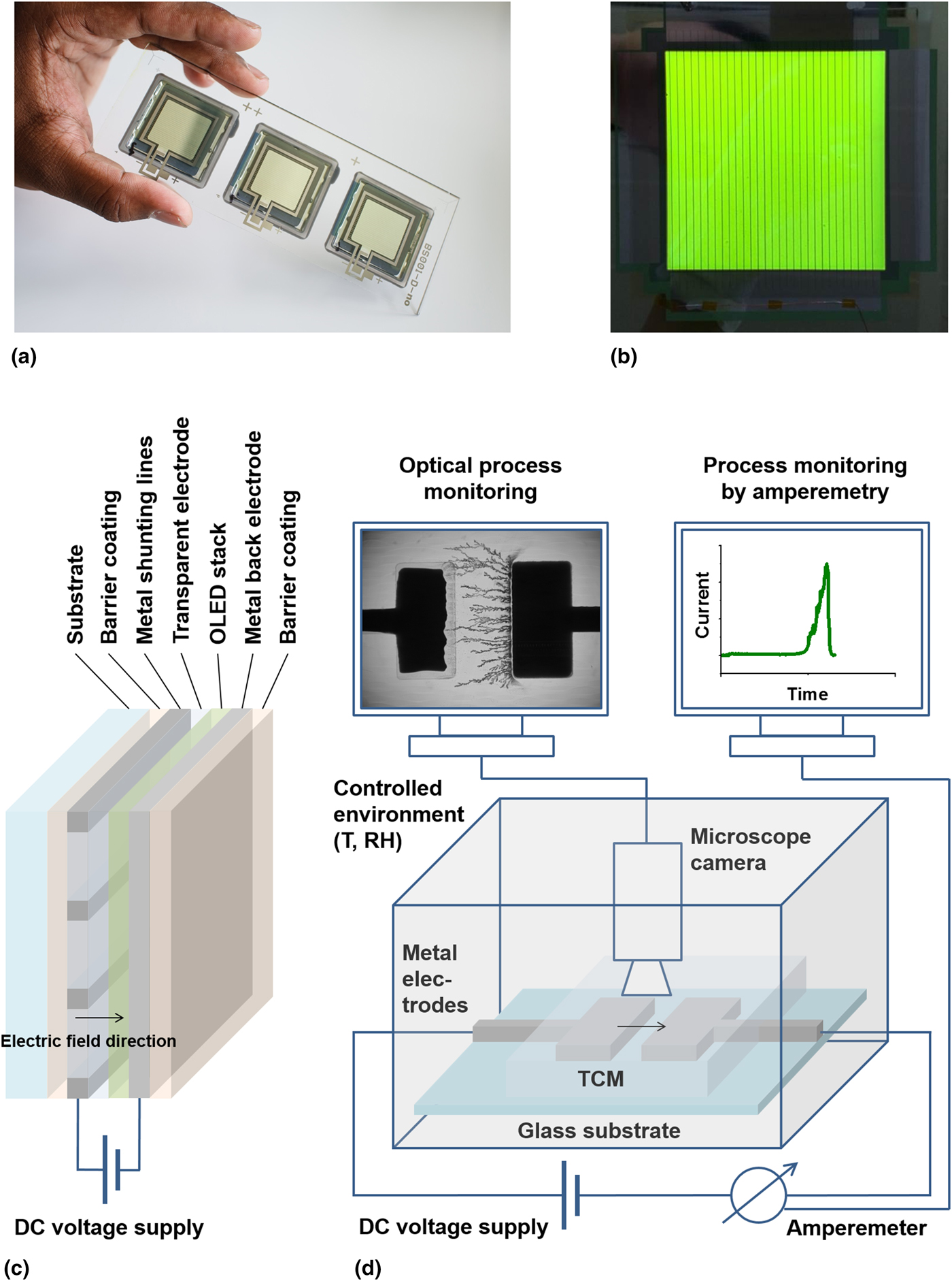
Silver is frequently employed in the electrodes of organic optoelectronic devices, such as organic light-emitting diodes (OLEDs) and photovoltaic cells. It is used as a continuous film, as Ag nanowire network or as shunting lines to reduce the resistive losses of transparent electrodes with insufficient intrinsic conductivities [Fig. 1(a–c)].[Reference Cao, Li, Chen and Xue6] Short circuiting by electrically induced Ag migration might therefore contribute to the limited lifetimes of organic optoelectronic devices containing Ag in one or both electrodes. Until now, however, studies dedicated to such migration processes within these device architectures have been rather scarce; those few published yielding controversial conclusions.[Reference Grandin, Tadayyon, Lennard, Griffiths, Coatsworth, Norton, Popovic, Aziz and Hu7–Reference Luo, Aziz, Popvic and Xu14] The reason is presumably that a direct study of these phenomena in complete devices is complicated by interference with competing failure mechanisms and the typically much localized formation of short circuits.
Experimental setup and its relation to OLED devices. (a, b) OLED devices containing Ag shunting lines. (c) Schematic illustration of the OLED device architecture. (d) Experimental setup for monitoring electrically induced metal migration through transparent conducting materials.

In this contribution, we present a study on metal (mainly Ag) migration under the influence of DC fields through thin poly(ethylenedioxy)thiophene:poly(styrenesulfonic acid) (PEDOT:PSS) films, a polymer electrolyte blend frequently used as transparent conductive material (TCM) for the electrodes of optoelectonic devices[Reference Cao, Li, Chen and Xue6] and as hole injection layer.[Reference Elschner, Kirchmeyer, Lövenich, Merker and Reuter15] With the experimental setup, metal migration can be studied isolated from other phenomena, and in addition, the formation of short circuits by metal dendrite growth can be easily monitored using amperometry and optical microscopy. We have studied both experimentally and by modeling the influence of various parameters such as the electric field strength and the composition of the TCM on the rate of short circuit formation and on the geometry of the formed metal dendrites. Finally, the outcome of these studies has been related to the degradation behavior of complete OLED devices.
Results and discussion
Experimental setup and process monitoring
The experimental setup used in this study is shown schematically in Fig. 1(d) and compared with a schematic representation of the OLED device architecture [Fig. 1(c)]. The latter, in its simplest configuration, consists of a layer of light-emitting material sandwiched between two electrodes, one of which is (semi)transparent and may contain metal shunting lines. By contrast, our test setup simply consists of two metal electrodes, the gap between which is filled with the TCM. This allows very easy observation of metal dendrite formation, because no opaque layers are blocking the view and the dimensions are in the hundreds of micrometers regime rather than tens of nanometers, as in actual devices.
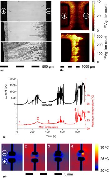
Using this setup, we were able to monitor the progress of electrically induced metal migration when a DC field was put across the interelectrode gap. Optical microscopy revealed the formation of dendrites, growing from the cathode to the anode, which at the same time gradually retracted [Fig. 2(a); Supplementary Movie S1]. This anode retraction indicates that Ag is removed from there by the migration process, but the transport of individual Ag atoms or ions cannot be visualized by our optical detection system. Therefore, we used Time-of-Flight Secondary Ion Mass Spectrometry (ToF-SIMS) analysis to determine the Ag distribution in the interelectrode space before dendrites were visible at the cathode. This revealed high Ag concentrations close to the anode, but not at the cathode [Fig. 2(b)], proving that the Ag migration process occurred from anode to cathode, i.e., in the direction of the electric field. Only upon reaching the cathode, the atoms form dendrites detectable by optical microscopy. This transport direction rules out electromigration by “electron wind” as the main transport mechanism in our system, which is in line with electrical conduction in PEDOT:PSS occurring primarily by hole transport.[Reference Elschner, Kirchmeyer, Lövenich, Merker and Reuter15] By contrast, electromigration by “hole wind”, which is more likely than “electron wind” to occur in PEDOT:PSS, and Ag ion migration following the electric field (i.e., electrochemical migration), cannot be distinguished solely based on the transport direction. Therefore, we have carried out a control experiment filling the interelectrode gap with PEDOT-free PSS, which is an electric insulator and thus not expected to allow any current flow. The fact that even in this system, dendrite formation at the cathode is observed (Supplementary Fig. S1), favors ion migration with the field rather than “hole wind” as the predominant transport mechanism.
Electrochemical migration monitoring. (a) Optical micrographs (back illumination) of the interelectrode space during Ag electrochemical migration through PEDOT:PSS at 30 V over a distance of 500 µm. (b) ToF-SIMS surface analysis of the 109Ag content of PEDOT:PSS present in the interelectrode space (1000 µm gap width) before (top) and after (bottom) 2 h of electrical stressing at 50 V. (c) Electrical current and maximum temperature monitored as a function of time (30 V over a distance of 500 µm) and (d) local temperature distributions (determined using an IR camera) at selected moments during this experiment [image numbers correspond to the moments accordingly marked in the bottom graph of (c)]. [In contrast to all other experiments reported in this paper, this measurement has not been performed with controlled RH, since the IR camera did not fit into the glove box. This is why the time to first short circuit formation is shorter than according to the data in (b).]

In parallel to the optical process monitoring, the current was also continuously measured, revealing a peak when the first dendrite touched the anode, forming a short circuit [Fig. 2(c)]. Obviously, the electrical connections did not last, suggesting that they broke due to overheating because of the locally very high-current densities. This interpretation was supported by spatially resolved temperature monitoring using an infrared (IR) camera, which showed local heating between the electrodes whenever high currents were observed [Fig. 2(c)/(d); Supplementary Movie S2]. As can be seen from Fig. 2(c), bursts of intense current flow and heat formation alternated with rather calm periods, with a general tendency of increasing current and temperature peaks during the course of the experiment.
To study the Ag electrochemical migration process in more detail, the electric field strength within the PEDOT:PSS was varied by changing both the interelectrode distance and the voltage across it. As a measure for the migration rate, the time until the first short circuit formation (“time-to-failure”) was taken [Fig. 3(a)]. As the relative humidity turned out to have a decisive influence on the process, all experiments were carried out under constant and controlled environmental conditions. In line with expectation, at constant voltage, larger gap widths resulted in longer migration times and at constant gap width, increasing the voltage accelerated the process [Fig. 3(b)]. Optical microscopic and scanning electron microscopy (SEM) images of the dendrites formed at 5 V over different interelectrode distances are displayed in Fig. 3(c) and (d). Very obviously, the shape of the dendritic structures was strongly influenced by the strength of the electric field: high fields (narrow gaps) gave rise to fine Ag structures well aligned with the field direction, indicating a dominating contribution of directed migration compared with lateral diffusion. By contrast, weaker fields (wider gaps) allowed relatively more lateral diffusion to occur, which is reflected in a stronger branching of the Ag dendrites. The structures obtained at lower fields were also significantly thicker and coarser. Cross-sectional SEM images of the formed dendrites showed that they were composed of porous material with grain sizes increasing with the gap distance (Supplementary Fig. S2).
Silver electrochemical migration through PEDOT:PSS. (a) Current flowing between the electrodes as a function of time at 30 V for different electrode spacings. (b) Dependence on voltage and electrode spacing of the time corresponding to occurrence of the first short circuit. (For 100 µm and 50 V, short circuit formation occurred too quickly to be reliably measured, which is why no data point is shown here. For 1000 µm and 30 V or lower, the experiments were stopped after 10,000 s, because short circuit formation had not yet occurred.) (c) Optical micrographs and SEM images of dendrites formed by Ag electrochemical migration at 5 V and varying the initial electrode spacing: 100 µm (top), 200 µm (center), and 500 µm (bottom). The white arrows mark the position of the original anode edge. (d) Optical micrographs of the electrodes and dendrites grown at 5 V between electrodes spaced at 200 µm (left) and 500 µm (right). (e) Graphical representations of simulated corrosion, migration and dendrite growth between electrodes initially spaced at 46 (left) and 190 (right) numerical grid points; polyelectrolyte medium, zero-valent metal, and cations are respectively represented in green, dark red, and blue. (f) Time to first short circuit plotted as a function of relative electrode spacing (open symbols: measured at different voltages, closed symbols: numerical simulations at a fixed voltage); the dashed lines represent fits to exponential functions.

Theoretical modeling
To gain understanding on how the dendrite morphology evolves as a function of voltage and electrode spacing, we modeled the process using a semi-discrete method describing diffusion-limited aggregation[Reference Chaikin and Lubensky16, Reference Uwaha and Saito17] in an electric field. The present model assumes ionization to be associated with an energy barrier that is lowered by the local electric field. It accounts for the coupling between electrode shape and dendrite morphology with the electric field by numerically solving the Poisson equation at each time step. Once a “metal atom”, represented by a single lattice site, has been ionized, it drifts toward the cathode where it becomes reduced. The ion leaves a vacancy in the anode at the location where it resided in its zero-valent state. This approach guarantees mass-conservation and automatically includes anode corrosion. The diffusive contribution to ion transport is accounted for by a Metropolis algorithm[Reference Metropolis, Rosenbluth, Rosenbluth, Teller and Teller18] biased by the local electric potential. We are aware of the fact that electrodeposition has been treated theoretically before.[Reference Chazalviel19–Reference Cogswell25] Although most of these studies include a more thorough electrochemical treatment, dendrite morphology is not considered in some cases.[Reference Chazalviel19–Reference Akolkar21] None of these studies considers corrosion-induced changes in electrode shape.
Figure 3(d) and (e) compare experimentally and computationally generated dendrite morphologies as a function of electrode spacing. Both the experimental Fig. 3(d) and computed Fig. 3(e) images represent the situation roughly when the first short circuit occurs due to dendrites crossing the gap. Experiment and calculation show that for a smaller electrode spacing the mean density of dendritic material in the gap increases. Further agreement between experiment and simulation is in the observation that with increasing electrode spacing the “splay” of the dendrites at the cathode becomes larger. For a small spacing the electric field becomes stronger and hence more directive. This is evidenced by the observation that the dendrites growing at the corners of the cathode follow the local curvature in the field lines. These morphological features are observed both in the experiment and the simulation.
Morphological differences between experimental and simulated structures, such as branching density, may be associated with the fact that the model does not account for a possible coupling between dendrite morphology and metal–polyelectrolyte interfacial tension,[Reference Cogswell25] matrix elasticity, and adhesion. Interestingly though, the experimentally observed tapering of the anode during the corrosion is fairly well reproduced by the model. We ascribe this phenomenon to locally accelerated corrosion at locations where field lines converge due to a high curvature of the metal interface.
Figure 3(f) provides a more quantitative comparison between experiment and calculation. This figure plots the time-to-failure (occurrence of the first dendrite–anode contact) against relative electrode spacing, for different voltages (experiment). The experimental data (open symbols) corresponds to physical time scales, whereas the calculated times (closed symbols) have been normalized by the time-to-failure at the smallest electrode spacing. Although an absolute comparison is not straightforward to make, the slopes of the experimental and simulated curves are quite similar, corresponding to an exponent of ~2. We conclude that despite its relative simplicity, the fair agreement with experimental data demonstrates the potential of our model to function as a predictive tool. Nevertheless, we consider further elaboration and more precise parametrization of its variables outside the scope of this study.
Influence of electrode materials on electrochemical migration
It has been reported that larger grain sizes stabilize metals against electrically induced migration.[Reference Ho and Kwok2] All experiments described so far have been carried out using evaporated Ag electrodes, which have a rather dense internal structure with large crystals. Electrodes prepared by printing nanoparticle-based conductive inks are much more porous, but thermal annealing after deposition can densify the structures and increase the grain sizes. Thus, such electrodes should be more prone to electrochemical migration than evaporated ones and this difference should decrease with harsher annealing conditions. We have therefore repeated our migration experiments using inkjet printed Ag electrodes, after having subjected them to varying annealing temperatures and times (Supplementary Table S1). The achieved specific electric conductivities ranged from 8% to 40% of the bulk Ag value (the evaporated samples reached 65%). As can be seen in Supplementary Fig. S3, the stability of printed and thermally annealed Ag electrodes towards electrochemical migration was clearly lower than for the evaporated ones. Within the printed samples, however, higher conductivity was related in a more complicated way to time-to-failure than anticipated. Instead of simply increasing with conductivity, the stability remained constant up to 20% of the bulk Ag value, and then a slight increase in stability was observed, before for 35% and 40%, the values even fell below the failure times at 20%. To explain this unexpected behavior, the solid content of the inks after solvent evaporation was subjected to thermogravimetric analysis at 225 and 300 °C, the two highest temperatures used to sinter the printed electrodes (Supplementary Fig. S4). It was observed that, after 2 h at 300 °C, a much larger fraction of the organic ink ingredients had degraded than at 225 °C. Although the function of these additives [mainly a coating of poly(vinyl pyrrolidone) for our system[Reference Abbel, van Lammeren, Hendriks, Ploegmakers, Rubingh, Meinders and Groen26]] is to stabilize the Ag nanoparticles in the unprocessed liquid ink by reducing their surface energy, it can be tentatively hypothesized that they do so as well after deposition and annealing. Although this assumption needs further experimental investigation, it makes comprehensible why electrodes exposed to higher temperatures actually exhibited lower stability toward electrochemical migration, despite their larger grain sizes and lower porosities.
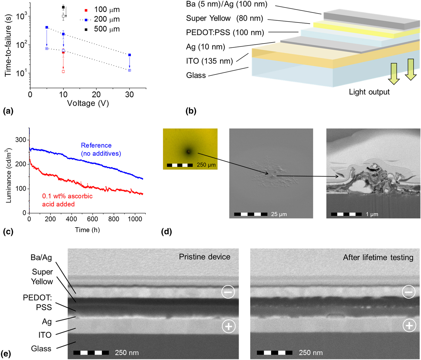
As in our system, the predominant migration mechanism is Ag cations following the electric field, we tried to retard or even suppress this process by adding a reducing agent (ascorbic acid) to the PEDOT:PSS. It was expected to convert the Ag cations into electrically neutral elemental metal, which will not be influenced by the electric field. In contrast to our expectations, however, the addition of 0.1 wt% of ascorbic acid to the PEDOT:PSS shortened the time-to-failure by a factor of two to five, as compared with the system without the additive [Fig. 4(a)]. Further experimental work, which is beyond the scope of the present study, will be necessary to investigate whether e.g., differences in the redox potentials of ascorbic acid and Ag ions between solution and solid state are responsible for this. Such changes have been reported earlier for other systems.[Reference Meerholz, Gregorius, Müllen and Heinze27]
(a) Influence of the addition of 0.1 wt% ascorbic acid to the PEDOT:PSS formulation. The filled squares correspond to the data shown in Fig. 3(b), the empty squares to the values with the additive under otherwise identical conditions. The arrows indicate the corresponding changes in time-to-failure. (b) OLED device architecture for lifetime testing. (c) Luminance output at constant current (50 mA) as a function of time for devices with and without ascorbic acid added to the PEDOT:PSS. (d) Optical micrograph and SEM images (top view and cross section) of a black spot, which had appeared after lifetime testing. (e) Cross-sectional SEM images of the OLEDs prior to (left) and after (right) lifetime testing (next to a black spot).

To demonstrate the applicability of our method to metals other than Ag, we have conducted migration experiments also using evaporated copper and palladium (Pd) electrodes. Although for copper the process turned out to be orders of magnitude slower than for Ag (days as opposed to seconds), nevertheless clear signs of dendrite formation were observed (Supplementary Fig. S5), indicating, consistent with literature,[Reference Zamanzadeh, Liu, Wynblatt and Warren28] that metal electrochemical migration is not limited merely to Ag. The geometric appearance of the copper dendrites was distinctly different than anything observed for Ag. No signs of metal displacement were observed for Pd electrodes, which is in line with the wide-spread use of Ag–Pd alloys to stabilize printed conductive structures against electrochemical migration.[Reference Yamamoto, Kakiuchi, Kashiwagi, Yoshida, Ohno and Nakamoto29]
As recently, Ag nanowire coatings have emerged as a novel solution-processable TCM,[Reference Cao, Li, Chen and Xue6] we have tested if these are also prone to electrochemical migration. For that reason, Pd electrodes, which do not show any migration by their own, have been covered with a network of Ag nanowires, and with PEDOT:PSS, as shown in Supplementary Fig. S6. Once a direct current was passed through that system, dendrite formation was observed at the Pd anode, indicating that also transparent electrodes composed of Ag nanowire networks can suffer from electrochemical migration.
Metal electrochemical migration in OLED devices
In a final set of experiments, we investigated in how far it was possible to transfer the results obtained with our simplified setup to lifetime predictions in actual OLED devices. To that end, OLEDs were prepared with Ag both present in the cathode and in the anode, and using PEDOT:PSS with and without 0.1 wt% of ascorbic acid as the transparent electrode material [Fig. 4(b)]. As the additive had shown an increase in migration rate through PEDOT:PSS, it was expected that this would lead to shorter operational device lifetimes, if Ag electrochemical migration contributed significantly to OLED performance degradation. No significant influence of the ascorbic acid on the transparency of the PEDOT:PSS was observed, whereas its sheet resistance decreased by a factor of two (Supplementary Table S2), a phenomenon also known from other additives containing hydroxyl groups.[Reference Nardes, Kemerkink, de Kok, Vinken, Maturova and Janssen30]
Functioning OLED devices could be prepared for both formulations; the exact performance characteristics are presented in Supplementary Table S2 and Fig. S7. When both types of devices were subjected to lifetime testing, it turned out that the reference devices’ performances were decreasing clearly more slowly than those of the OLEDs containing ascorbic acid [Fig. 4(c)]. Microscopic analysis of the samples after lifetime testing revealed that black spots had formed in the case of the devices containing ascorbic acid, whereas this phenomenon was not observed in the reference devices. Electron microscopic analysis of such a defect showed a total destruction of the functional layer structure directly at these spots [Fig. 4(d)]. Although this finding is not inconsistent with the explanation of a short circuit having been formed and subsequently burnt through, the damage was too severe to clearly prove Ag electrochemical migration having occurred prior to failure. Cross-sectional SEM analysis on the still emissive area next to the black spot, however, revealed clearly the accumulation of Ag at the interface between PEDOT:PSS and the light-emitting polymer when compared with an identical device that had not undergone lifetime testing [Fig. 4(e)]. In addition, Ag also seemed to have been transported all the way through the PEDOT:PSS and deposited at the Ba/Ag cathode. Finally, bubbles or voids were formed in the Ag layer on the indium tin oxide anode, suggesting Ag removal. These observations are consistent with our proposal that the device deterioration and black spot formation were caused by Ag electrochemical migration leading to localized device failure. As at current state, however, several competing explanations cannot be definitely excluded, further research is needed to definitely confirm or disprove this hypothesis. Additionally, more detailed investigations are also necessary to elucidate the exact mechanism of the ascorbic acid's effects on the electrochemical migration behavior of Ag in both pure PEDOT:PSS and in OLED devices.
Conclusion
In summary, we have developed an experimental setup, which allows us to continuously monitor electrically induced metal migration through TCMs in a much more convenient manner than in complete devices. Reducing the number of components to a pair of electrodes and a TCM has enabled us to design a simplified model system, in which metal migration is the only occurring failure mechanism and can be studied without interference from competing processes. The geometric arrangement of the electrodes allows techniques such as optical and IR microscopy in addition to amperometry to be applied for process monitoring. In this way, the growth of metal dendrites spanning the interelectrode space can be correlated to the observation of peaks in local temperatures and electric currents, which are indicative of short circuit formation. A number of parameters such as field strength, electrode material, and composition of the TCMs have been varied, and their influence on migration speed and dendrite appearance has been studied. The results support the assumption of electrochemical migration rather than electromigration being the predominant transport mechanism in this system. I.e., Ag+ ions are detached from the anode and transported to the cathode under the influence of a DC field, whereas no indications for electromigration by “charge carrier wind” have been found. Upon hitting the cathode, the metal is attached there and forms dendrites, which grow opposite to the migration direction until both electrodes are short circuited. Finally, initial studies were undertaken to correlate the results from the experimental setup with lifetime tests of actual OLED devices. These support the assumption that experiments using the simplified test setup can contribute to the understanding of OLED failure mechanisms. In the future, this setup might be used to efficiently screen and optimize large numbers of candidate strategies for slowing down or totally suppressing metal electrochemical migration, with only the most promising ones actually being tested in full OLED devices.
Supplementary material
The supplementary material for this article can be found at https://doi.org/10.1557/mrc.2017.46
Acknowledgements
The authors are grateful to Jaquelien van den Boomen and Chantal van Berkel for their practical support with the experimental work described in this study. The research presented here has received partial funding from the European Union's Seventh Framework Programme (FP7/2007-2013) under the grant agreement no. 31011 (Light Touch Matters project LTM).