
Introduction
Organic–inorganic hybrid lead (II) halide perovskites attracted significant interests in photovoltaic devices owing to their easy accessibility, low defect density, excellent charge transport properties, and high-power conversion efficiency.[Reference Kojima, Teshima, Shirai and Miyasaka1–Reference Zhou, Chen, Li, Luo, Song, Duan, Hong, You, Liu and Yang3] However, fast degradation of properties under the influence of environmental factors such as humidity,[Reference Yang, Siempelkamp, Liu and Kelly4] light,[Reference Wang, Wright, Elumalai and Uddin5] and heat[Reference Kumar and Dhar6] are some of the major obstacles toward commercialization of perovskite materials. Previous attempts to enhance the environmental stability that involve incorporation of pseudohalogens,[Reference Jiang, Rebollar, Gong, Piacentino, Zheng and Xu7] surface passivation with a capping agent,[Reference Yang, Wang, Liu, Cheng, Zhao and Yang8] and use of different methods of fabrication[Reference Niu, Li, Meng, Wang, Donga and Qiu9, Reference Zheng, Chung, Ma, Zhang, Xiao, Chen, Wang, Qu and Gong10] were successful, but not enough to enhance the stability of hybrid perovskite for immersing in water, which is prerequisite for many electrochemical applications. One of the tried and tested methods to improve the stability and efficiency of perovskite materials include growing a shell of another semiconductor,[Reference Da, Cha, Sun, Wu, Wang and Zheng11] hydrophobic molecules[Reference Kim, Jo, Kim, Jang, Kang, Lee, Kim, Jun and Lee12] around the particles, to develop core–shell nanocrystals, or use of external passivating layers.[Reference Dirin, Dreyfuss, Bodnarchuk, Nedelcu, Papagiorgis, Itskos and Kovalenko13, Reference Hwang, Jeong, Lee, Ko and Yong14] Recently, a few hydrophobic polymer coatings have been used to protect perovskite nanoparticles from the water.[Reference Guarnera, Abate, Zhang, Foster, Richardson, Petrozza and Snaith15] Such coatings imposed an overwhelming electronic barrier on hybrid perovskite materials toward most photoelectrochemical (PEC) applications. In addition, these reported methods work well for solar cell application, but none of them is suitable as a universal method for stabilizing the perovskite nanocrystals inside water and perform the water-splitting reaction.
Here we report an in situ synthesis, characterization, and use of a hydrophobic shell of 4-[(N-3-butyne)carboxyamido]anilinium lead iodide (NBCAnPbI3) to encapsulate MAPbI3 perovskite crystals. The alkyne groups present in the shell induce sufficient hydrophobicity to prevent the diffusion of water from outside and protect MAPbI3 crystals. This shell also possesses conduction band edge favorable for electron transfer from MAPbI3 to outside electrodes, which is important to maintain the photosensitizing property of perovskite material. This unique combination of fascinating water stability and suitable band position make this assembly optimum for PEC reactions such as water splitting.
Experimental section
Full details of materials and methodologies are given in the Supplementary information.
Synthesis of NBCAnPbI3 encapsulated CH3NH3PbI3
First precursor solution was prepared by mixing of CH3NH3I (MAI, 0.196 g, 1.23 mmol), 4-carboxyanilinium iodide (CAnI, 0.326 g, 1.23 mmol), and PbI2 (1.134 g, 2.46 mmol) in 2 ml of γ-butyrolactone at 60 °C for 12 h. 1-Amino-3-butyne (12.3 mmol) and the coupling agent 1-ethyl-3-(3-dimethylaminopropyl)carbodiimide (EDC, 5 mg, 0.026 mmol) were added to the above solution for full conversion of −COOH to −CO-NH− group. The solution was stirred at room temperature for 18 h for 3 days, with periodic monitoring. The precipitated solid was collected and heated at 85 °C for 20 h to remove the residual solvent. A gradual shift of color from yellow to brown was observed during the heating and the dry powder was used for further characterization. A similar procedure was adopted to make a control perovskite sample, NBCAnPbI3 for comparison of properties.
Synthesis of 0.5 NBCAnPbI3{1 MAPbI3}
This mixed perovskite was prepared by mixing CAnI and MAI in a ratio of 0.5:1 with stoichiometric amounts of PbI2, followed by EDC-assisted alkyne functionalization, as described above.
Synthesis of MAPbI3, CAnPbI3 {MAPbI3}, and TPbI3{MAPbI3}
To prepare a control sample of pure MAPbI3, a reported literature procedure was followed.[Reference Kim, Lee, Im, Lee, Moehl, Marchioro, Moon, Humphry-Baker, Yum, Moser, Grätzel and Park16] CAnPbI3{CH3NH3PbI3} was prepared by heating the stoichiometric mixture of CAnI, MAI, and PbI2 dissolved in γ-butyrolactone (2 mL) at 60 °C for 12 h at 80 °C till drying. p-Toluidinium lead (II) iodide (TPbI3)-encapsulated MAPbI3 (TPbI3{MAPbI3}) was prepared by mixing equimolar amounts of 4-toluidinium iodide (TI) and MAI along with the stoichiometric amounts of PbI2 dissolved in γ-butyrolactone (2 mL) at 60 °C for 12 h. The precipitated solid was collected and heated at 80 °C to remove the excess solvent. The dry samples were used for further characterization.
Fabrication of photoanode
Fabrication of photoanode includes following steps: p25-TiO2 paste (5 g, Degussa p25 powder) was prepared using the previously mentioned method.[Reference Ito, Chen, Comte, Nazeeruddin, Liska, Pechy and Grätzel17] A thin film of TiO2 was cast over a cleaned ITO substrate (0.24 cm2), followed by calcination at 450 °C for 30 min. A slurry of NBCAnPbI3{MAPbI3} in γ-butyrolactone was spread over p25-TiO2 film and heated at 85 °C for 20 h. In the third step, 0.1 g p25-TiO2 paste (ethanol as solvent) was coated followed by heating at 85 °C for 60 min over NBCAnPbI3{MAPbI3}.
Results and discussion
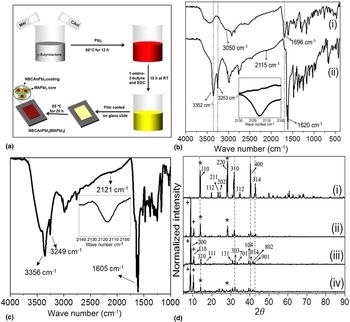
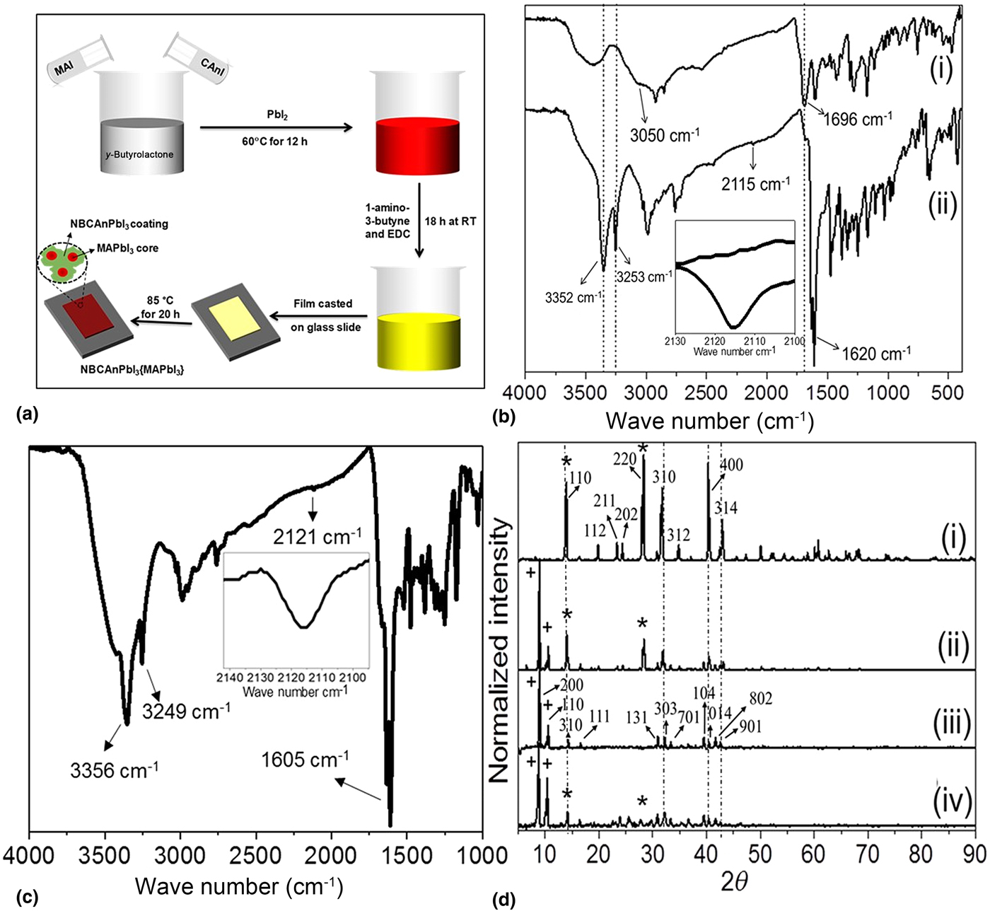
The precursor solution was prepared by mixing MAI, CAnI, and PbI2 in 2 mL of γ-butyrolactone, heated at 60 °C for 12 h. 1-Amino-3-butyne was then coupled in situ to a −COOH group of CAnI to get the final product. The procedure was demonstrated via a schematic diagram [Fig. 1(a)] and discussed in detail in the “Experimental” section.
(a) Schematic representation of synthetic approach for the encapsulated MAPbI3. (b) FTIR spectra of mixed perovskites before (i) and after (ii) amide linkage formation using EDC coupling. The inset shows the presence of C≡C stretching peak (~2115 cm−1) of the spectrum. (c) FTIR spectra of pure NBCAnPbI3. The inset shows the presence of C≡C stretching peak (~2121 cm−1). (d) Powder XRD patterns of MAPbI3 (i), NBCAnPbI3{MAPbI3} (0.5:1) (ii), pure NBCAnPbI3 (iii), NBCAnPbI3{MAPbI3} (1:1) (iv), (+marks show two major peaks of NBCAnPbI3. Dotted lines, specially the * mark, indicate the presence of MAPbI3 in all samples except pure NBCAnPbI3). The intensity of XRD peaks of MAPbI3 gradually reduced with an increase in NBCAnPbI3 amount in the mixed sample.
Functionalization and proof of encapsulation
Successful alkyne functionalization via amide linkage between CAnI and 1-amino-3-butyne was demonstrated using Fourier-transform infrared spectroscopy (FTIR) spectra [Fig. 1(b)]. Amide-NH (~3352 cm−1) and amide >C=O (~1620 cm−1) along with terminal C≡C–H (~3253 cm−1), C≡C (~2115 cm−1) stretching frequencies in the spectrum of the product after functionalization confirms the alkyne group incorporation through acid–amine coupling reaction. The absence of broad −OH vibrations and shift of >C=O peak (from 1696 to 1620 cm−1) in the IR spectra of the samples before and after functionalization showed the transformation of acid to amide groups in the final product. To prove the chemical formula of alkyne functionalized 4-carboxyanilinium lead iodide, same acid–amine coupling reaction was performed without adding MAI (see the Experimental section) and check with x-ray photoelectron spectroscopy (XPS). After successful alkyne functionalization [Fig. 1(c)], XPS survey scan performed at different regions of the sample revealed the presence of lead (Pb) and iodine (I) with an atomic ratio of 1:3 (Fig. S1). This 1:3 ratio of Pb:I along with successful alkyne functionalization indicates a possible molecular formula of our functionalized material as NBCAnPbI3. The x-ray diffraction (XRD) pattern of NBCAnPbI3 was indexed using TREOR software, which indicates an orthorhombic (Pmmn) crystal structure with lattice parameters, a = 19.6442, b = 9.244, and c = 9.1901. As we used MAI with a stoichiometric amount of PbI2 along with the precursors of NBCAnPbI3, the formation of a hybrid phase material NBCAnPbI3{MAPbI3} is investigated using XRD. The powder XRD data [Fig. 1(d)] of the target material, NBCAnPbI3{MAPbI3}, were compared with homogeneous pure MAPbI3 and NBCAnPbI3 to identify the presence of both components in the final product. The presence of multiple diffraction peaks of MAPbI3 in NBCAnPbI3{MAPbI3} shown by a dotted line and * marks indicate the presence of MAPbI3 in our target material NBCAnPbI3{MAPbI3}. Although some of the diffraction peaks of MAPbI3 overlapped with the diffraction peaks of NBCAnPbI3, the presence of two major diffraction peaks 110 and 220 (* marked) of MAPbI3 in NBCAnPbI3{MAPbI3} indicates the presence of tetragonal phase of MAPbI3[Reference Oku18] in our target material NBCAnPbI3{MAPbI3}. The diffraction peaks of the most intense peaks (marked as +) corresponding to the (200) and (110) planes of NBCAnPbI3 indicate the presence of NBCAnPbI3 phases inside the hybrid material NBCAnPbI3{MAPbI3}. In addition, the hybrid materials prepared with a reduced molar ratio 1:0.5 for MAI:CAnI (see the Experimental section), followed by functionalization with 1-amino-3-butyne, led to the formation of both phases in the sample with reduced water stability. Moreover, UV–vis spectra of pure MAPbI3 (Fig. S2, i) and NBCAnPbI3 (Fig. S2, ii) were compared with NBCAnPbI3{MAPbI3}(Fig. S2, iii). The broad and strong absorption of NBCAnPbI3{MAPbI3} (Fig. S2, iii) in the longer wavelength region indicate the presence of both MAPbI3 and NBCAnPbI3 in the material.
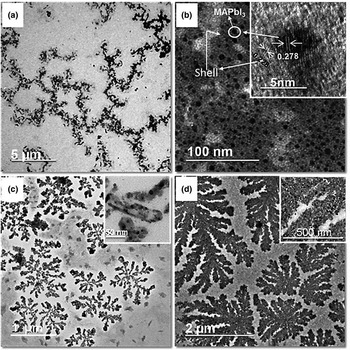
The formation of NBCAnPbI3 shell over MAPbI3 was investigated by transmission electron microscopy [TEM, Fig. 2(a)], which showed the presence of a well-connected network structure, instead of discrete particles. The presence of network structure implies an encapsulated architecture for the final materials, rather than the formation of a physical mixture of two different materials. Higher magnification image of the materials [Fig. 2(b)] indicates the presence of materials encapsulating discrete darker particles. High-resolution TEM micrograph of a dark spot [inset of Fig. 2(b)] shows lattice fringes with a d-value of ~0.278 nm, which matches with the (310) plane of tetragonal MAPbI3[Reference Oku18] and brighter spot having a d-value of ~0.228 nm, which corresponds to the (104) plane of orthorhombic NBCAnPbI3. No such encapsulating structure and the presence of discrete dark particles with 0.278 nm d-spacing were observed in the TEM micrographs of pure MAPbI3 (Fig. S3). The control samples prepared using TI and CAnI using the same procedure (see the Experimental section) were also fully characterized and properties were compared. TEM micrographs of both CAnPbI3{MAPbI3} [Fig. 2(c)] and TPbI3{MAPbI3} [Fig. 2(d)] showed similar encapsulated structures with less extended architectures than the previously discussed NBCAnPbI3{MAPbI3}. This discrepancy in network structure formation could be attributed to different diffusion-limited aggregation (DLA) growth[Reference Maxim, Ferreira, Vilarinho and Reaney19] in the presence of phenylammonium cations. The microstructure of the in situ generated bilayer is suggestive of classical DLA of CAnPbI3 over MAPbI3 [Fig. 2(c)] as well as TPbI3 over MAPbI3 [Fig. 2(d)]. Such a growth mechanism is prevalent in systems that have anisotropic diffusion coefficient of molecular species (in this case CAnPbI3 and TPbI3) due to structural heterogeneity (e.g., diffusion coefficient at a step-“edge” can be less than the diffusion coefficient on a “planar” step). This random walk of molecules and irreversible sticking to the perimeter of growing aggregates is already discussed in a previous literature.[Reference Brune, Romainczyk, Roder and Kern20] The variation of sticking coefficient (K stick) and change in cluster shape also explained earlier.[Reference Ranguelov, Goranova, Tonchev and Yakimova21] Also, lowering the value of K stick affects the capture activity of branches of growing aggregates and channelize the diffusion toward center[Reference Ranguelov, Goranova, Tonchev and Yakimova21] to produce a network structure of NBCAnPbI3{MAPbI3} shown in Figs. 2(a) and 2(b). To identify the presence of different phases in the control samples, we performed powder XRD analyses (Fig. S4) of CAnPbI3{MAPbI3} and TPbI3{MAPbI3} perovskites. The peaks marked with a star in Fig. S4 indicate the presence of MAPbI3 in both the materials. As expected, comparison of powder XRD data of pure CAnPbI3 or TPbI3 with mixed samples CAnPbI3{MAPbI3} and TPbI3{MAPbI3} showed the presence of phases corresponding to all components in the final samples (Fig. S4).
TEM micrographs of (a) network of NBCAnPbI3{MAPbI3} and (b) magnified image of the network. The inset in (b) shows high-resolution micrograph where fringes of the dark spot with a d-spacing ~0.278 nm corresponding to the tetragonal MAPbI3 and brighter region with a d-spacing ~0.228 nm corresponds to the shell of orthorhombic NBCAnPbI3 (c) CAnPbI3{MAPbI3} and (d) TPbI3{MAPbI3} with their magnified images are shown in the inset.

Investigation of water stability
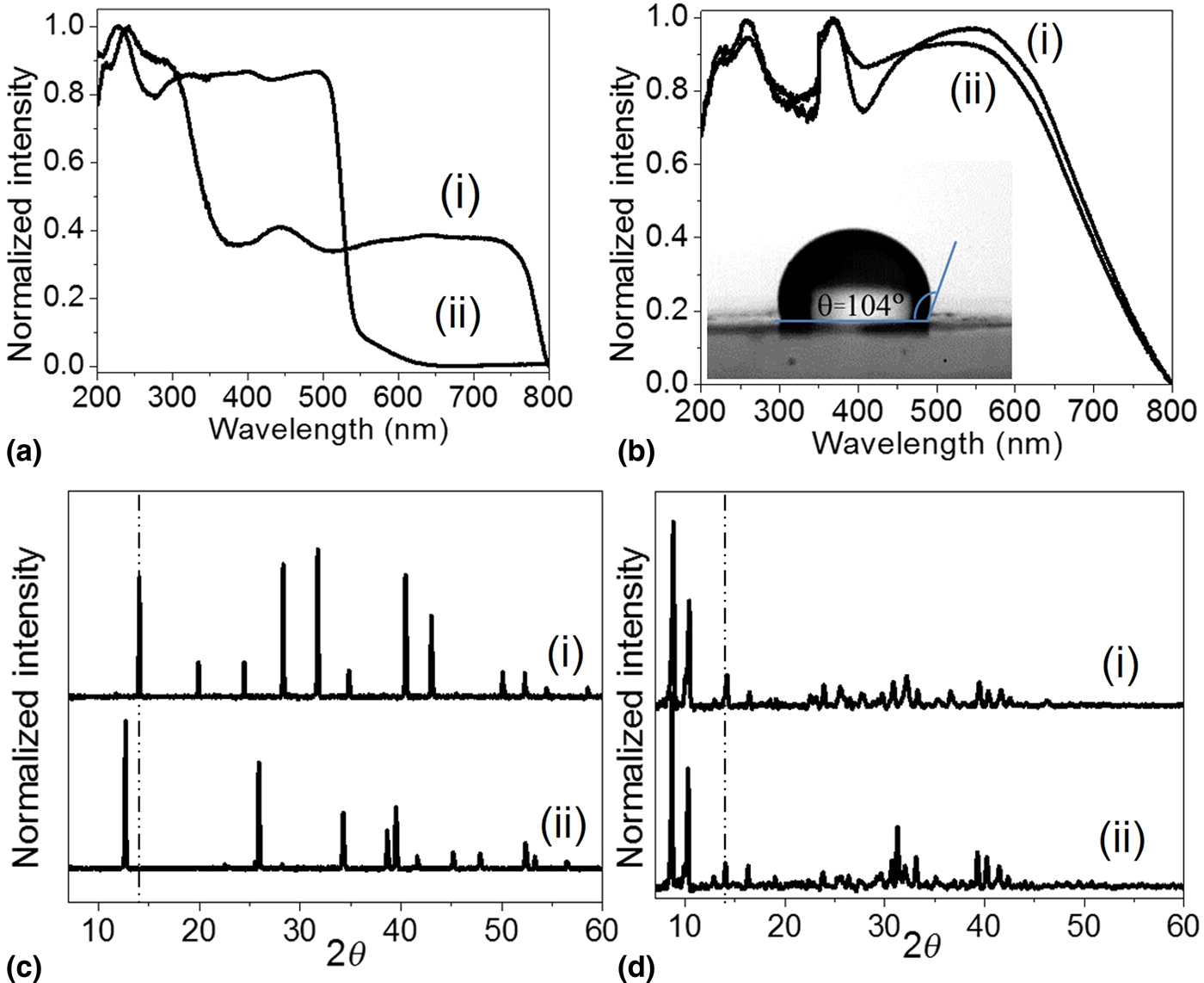
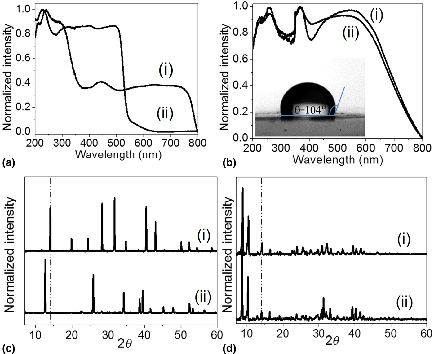
Extended network formation observed for NBCAnPbI3{MAPbI3} in TEM micrographs motivated us to investigate the water stability and compare with the established MAPbI3 material. The black color of the material turns to yellow as soon as MAPbI3 was immersed in water, which can also be monitored by UV–vis spectroscopy [Fig. 3(a)]. At the same time, no significant changes in colors were observed in the case of NBCAnPbI3{MAPbI3} after immersing in water for 30 min [Fig. 3(b)], which indicates high water stability of the target hybrid material. The instability of conventional MAPbI3 was further checked by dipping the film in water just for 30 s and monitored by XRD. The disappearance of all the characteristic diffraction peaks and appearance of completely new diffraction pattern shown in Fig. 3(c) proved that even 30 s of water immersion is sufficient to break tetragonal packing of MAPbI3 led to the formation of PbI2,[Reference Yang, Siempelkamp, Liu and Kelly4] whereas minimum differences in powder XRD data before and after immersion in water for as long as 30 min [Fig. 3(d)] confirm the stability of NBCAnPbI3{MAPbI3}. To check the moisture stability of the NBCAnPbI3{MAPbI3}, the sample was kept inside a humidity chamber under 95% humidity for several days. Systematic XRD study of the test material exposed to moisture indicated no changes in the crystal structure (Fig. S5) within the first 10 days, which points to the high stability against moisture. The higher stability of the hybrid NBCAnPbI3{MAPbI3} perovskite toward humidity and water is due to the hydrophobicity of the shell, which is confirmed by contact angle measurements. NBCAnPbI3{MAPbI3} showed a higher contact angle [~104°, inset in Fig. 3(b)] as compared with hydrophilic MAPbI3 (contact angle decreases quickly from 51ο to 33ο and stabilizes at 27ο).[Reference Yang, Wang, Liu, Cheng, Zhao and Yang8] The instabilities of control samples, CAnPbI3{MAPbI3} and TPbI3{MAPbI3}, in water indicate the importance of incorporation of hydrophobic alkyne functionalization.
UV–vis spectra of MAPbI3 (a) and NBCAnPbI3{MAPbI3} (b) before (i) and after (ii) immersion in water. The inset shows the contact angle which was measured by placing a drop of water on top of the sample and recording the image using CCD camera. XRD spectra of MAPbI3 (c) and NBCAnPbI3{MAPbI3} (d) before (i) and after (ii) immersion in water. Dotted lines represent the (110) plane of conventional MAPbI3 indicating the presence or absence of MAPbI3 in the system.
Proof of concept demonstration of water splitting with high applied bias photon-to-current efficiency (ABPE)
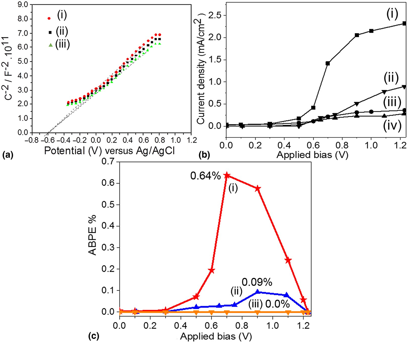
Since NBCAnPbI3{MAPbI3} is stable in water, the conduction band edge position of the shell material, NBCAnPbI3, needs to be measured before performing an electrochemical reaction using the new mixed perovskite material. The standard electrochemical methods based on impedance spectroscopy and Mott–Schottky equation were used to calculate the flat band potential (see the Experimental section). NBCAnPbI3-coated ITO was used as working electrode, Pt wire mesh, and Ag/AgCl electrode as a counter and reference electrodes, respectively. K3[Fe(CN)6] (7 × 10⁻⁴ M) dissolved in 1 M KCl solution was used as electrolyte to record impedance spectra. Mott–Schottky plot was prepared using a previously published procedure.[Reference Gelderman, Lee and Donne22] The point of intersection is independent of frequencies applied, and the flat band potential of NBCAnPbI3 calculated from intersection point is ~−0.6 V versus Ag/AgCl [−0.403 V versus normal hydrogen electrode (NHE)] [Fig. 4(a)]. The potential value conversion from NHE to vacuum was done by using conventional methods described in the literature.[Reference Grätzel23] The calculated conduction band of NBCAnPbI3 is −4.1 eV close to the conduction band of TiO2 and lower than that of MAPbI3,[Reference Aharon, Dymshits, Rotem and Edgar24] which enables the photogenerated electrons of MAPbI3 to pass through the shell and available for electrochemical processes.
(a) Mott–Schottky plot for NBCAnPbI3 measured at different frequencies (i) 1526 Hz, (ii) 954 Hz, (iii) 595 Hz, which indicates the flat band position at ~−0.6 V versus Ag/AgCl. (b) Two electrode analysis for photoelectrochemical water splitting using NBCAnPbI3{MAPbI3} as a sensitizer (i = current under solar radiation, iii = dark current) and only with p25-TiO2 (ii = current under solar radiation, iv = dark current). (c) Applied bias photo-to-current efficiency of p25-TiO2 photoanode in the presence of NBCAnPbI3{MAPbI3} (i), p25-TiO2 only (ii), and in the presence of NBCAnPbI3 (iii).
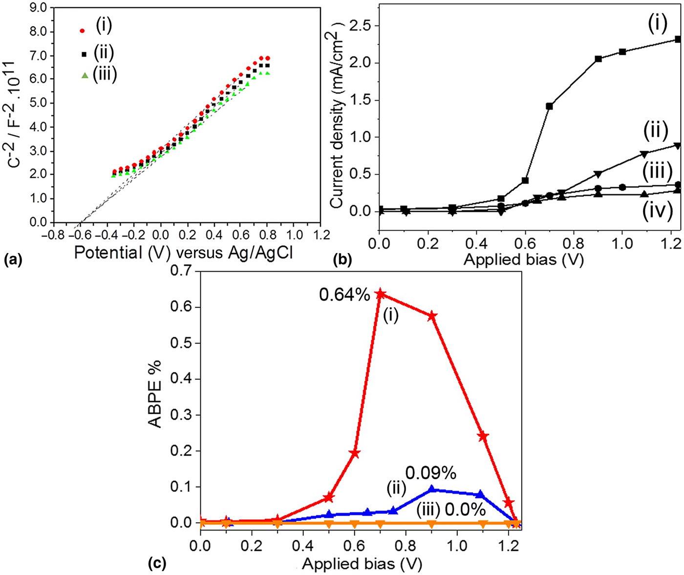
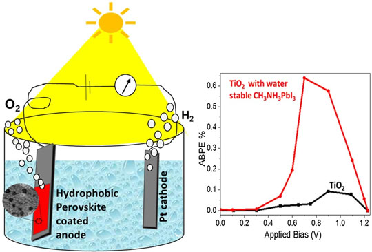
Favorable band position and water stability of NBCAnPbI3{MAPbI3} imply the hybrid material to act as a sensitizer in the PEC application. As a proof of concept, the water-splitting reaction using the hybrid perovskite material as a sensitizer is demonstrated below. Details of photoanode fabrication are discussed in the Experimental section. A thin layer of commercial p25-TiO2 was coated over NBCAnPbI3{MAPbI3} to facilitate oxygen evolution reaction and to regenerate the NBCAnPbI3{MAPbI3} by photogenerated electrons. The performance of fabricated heterostructures has been evaluated using a standard two probe method.[Reference Hisatomi, Kubota and Domen25] Under dark conditions, the thermodynamic requirement for water splitting is 1.23 V and a higher potential is required for effective water splitting due to overpotentials. However, in the presence of light, a good photosensitizer generates electrochemical bias from solar light such that the sum of the generated and applied electrochemical bias is >1.23 V. It is known that p25-TiO2 is a mediocre PEC catalyst due to its high band gap,[Reference Daghrir, Drogui and Rober26] which is unable to show major changes in current in the presence and absence of light. On the contrary, a significant increase in photocurrent in the presence of NBCAnPbI3{MAPbI3}-coated p25-TiO2 was observed, which implies the sensitizing capability of mixed perovskite [Fig. 4(b)]. To further quantitatively demonstrate the improved performance of photoanode, applied bias photon-to-current efficiency (ABPE) was evaluated using standard methods.[Reference Chen, Jaramillo, Deutsch, Kleiman-Shwarsctein, Forman, Gaillard, Garland, Takanabe, Heske, Sunkara, McFarland, Domen, Miller, Turner and Dinh27] The ABPE efficiency was calculated to evaluate PEC cell performance under external potential using Eq. (1) given below.
 $${\rm ABPE} = \left[ {\displaystyle{{ \vert j_{{\rm ph\;}} ({\rm mA\; cm}^{ - 2} ) \vert \times (1.23 - \vert V_{\rm b} \vert )\; ({\rm V})} \over {P_{{\rm total}} ({\rm mWcm}^{ - 2} {\rm \;} )}}} \right]_{{\rm AM 1}.{\rm 5G}} $$
where j ph is the photocurrent density, V b is the applied bias between working and counter electrodes, and P total is the incident illumination power density (AM1.5G, 100 mW/cm2). Since photocurrent achieved at low applied bias values play a significant role to understand the efficiency of a photoactive material, we have estimated the activity of the photoactive assembly by measuring applied bias between the counter and working electrodes below the thermodynamic potential of water (1.23 V), at which the maximum photon-to-current conversion is achieved.[Reference Upadhyay, Behara, Sharma, Gyanprakash, Pala and Sivakumar28] ABPE of 0.64% was achieved by the photoanode in the presence of NBCAnPbI3{MAPbI3} [Fig. 4(c, i)], whereas ABPE value drops to 0.09% in the absence of NBCAnPbI3{MAPbI3} coating [Fig. 4(c, ii)]. A drastic improvement (~seven times) of ABPE in the presence of the hybrid perovskite indicates the important role of NBCAnPbI3{MAPbI3} as a sensitizing material. Moreover, no such photoresponsive behavior was achieved without the presence of MAPbI3 (presence of only shell NBCAnPbI3), which is clearly represented by 0% ABPE shown in Fig. 4(c, iii), which unerringly proved the sensitizing role of MAPbI3 to achieve high ABPE. We attribute this enhancement to much higher photon absorption and diffusion length of the MAPbI3[Reference Yang, Siempelkamp, Liu and Kelly4] core present in NBCAnPbI3{MAPbI3}. Facile e−–h+ pair separation is possible due to the favorable band position of NBCAnPbI3, calculated using Mott–Schottky plot [Fig. 4(a)] with respect to the band position of MAPbI3 and TiO2.[Reference Aharon, Dymshits, Rotem and Edgar24] The calculated conduction band of NBCAnPbI3 is −4.1 eV close to the conduction band of TiO2 and lower than that of MAPbI3,[Reference Aharon, Dymshits, Rotem and Edgar24] which enable photogenerated electrons of MAPbI3 to pass swiftly to TiO2 electrode and allow MAPbI3 to be regenerated by photogenerated electrons from p25-TiO2 (Fig. S6). Both these effects are responsible for facile e−–h+ pair separation for PEC water splitting with ~seven times increment of ABPE value [Fig. 4(c)]. Gas evolved from anode during the electrochemical reaction was identified as oxygen and bubbles generated at Pt cathode as H2, confirming the water-splitting reaction instead of any other reaction inside the cell[Reference Gao, Ding, Liu, Wang, Lu, Li and Sun29] (Fig. S7). It is also true that limited regeneration of NBCAnPbI3{MAPbI3} by p25-TiO2 is responsible for the slow oxygen evolution.[Reference Wang, Zhong, Qin and Zhang30] Such drawback can limit the photocurrent and reduces the life of the cell, as observed by the reduction in current density at a constant potential of 0.5 V (Fig. S8). This is corrected by adding methylene blue (MB) as a sacrificial agent.[Reference Ji, Jang, Cho, Myung, Kim, Kim and Park31] Chronoamperometry measurements in the presence of MB showed a constant current density over a period of time as compared with the data collected without MB (Fig. S8). We are currently optimizing the performance of the materials and further investigation involving the fabrication of cells with good oxygen evolution properties.
Conclusion
In conclusion, we have deposited a hydrophobic shell of NBCAnPbI3 over MAPbI3 to enhance the stability in water under immersed condition. Alkyne functional groups play a crucial role toward introducing hydrophobicity with a large contact angle of ~104°. More importantly, suitable conduction band position of this crystalline network allows facile electron transfer from MAPbI3 to TiO2 and makes the whole assembly suitable for PEC applications. Interestingly, a 7-fold increase in ABPE value was observed than conventional p25-TiO2 in the presence of NBCAnPbI3-encapsulated MAPbI3 as a sensitizer. We hope this study will open a new avenue of applications for perovskite materials in water splitting and photocatalytic hydrogen evolution, where immersion of electrodes in water is needed.
Supplementary material
The supplementary material for this article can be found at https://doi.org/10.1557/mrc.2018.56
Acknowledgments
The authors gratefully acknowledge the financial support from the Technology System Development program of the Department of Science and Technology, Government of India via project DST/TSG/SH/2011/106. S. S. and S. V. acknowledge the funding support from the National University of Singapore under the joint Ph.D. program between NUS and IITK. S. S. K. acknowledges the Centre for Environmental Science & Engineering, Thematic Unit of Excellence on Soft Nanofabrication, IITK.