I. INTRODUCTION
Single-walled carbon nanotubes (SWCNTs) can be visualized as a seamless cylinder rolled up by 1-atom-thick planar graphene sheet. They can be either metallic (m) or semiconducting (s) depending on the rolling direction of the graphene sheet. m-SWCNTs can carry an electrical current density, which is three orders of magnitude higher than a typical metal, such as copper or aluminum at ∼4 × 10⁹ A/cm2,Reference Zhou, Park, Huang, Liu and McEuen1 and the carrier mobility of individual s-SWCNTs is ten times better than that of silicon at ∼10,000 cm2/(V s2).Reference Dai, Javey, Pop, Mann, Kim and Lu2 Such exceptional electronic properties inspire intensive research on many of their potential applications, including conductive films, interconnects, transistors, logic gates, and sensors. Most of these applications need uniform m- or s-SWCNTs; e.g., SWCNT-based transistors need high purity s-SWCNTs. However, none of the current synthesis methods can produce SWCNTs with uniform metallicity or structure. To overcome this barrier, significant research efforts have been dedicated to separate and enrich SWCNTs according to their diameter, metallicity, and chirality.Reference Banerjee, Hemraj-Benny and Wong3–Reference Liu and Hersam5
SWCNT networks have shown great potentials in realizing the transistor applications of SWCNTs.Reference Yang, Kong, Jung, Baek, Han, Oh and Jung6, Reference Cao and Rogers7 Compared with transistors using individual tubes, SWCNT networks average the electronic properties of many SWCNTs, and the chance of forming conducting paths is significantly reduced. Besides, it is also much easier to achieve scalable production of SWCNT thin films at fairly low cost comparing with positioning and aligning many individual tubes.Reference Lay, Novak and Snow8 SWCNT structures, such as metallicity, diameter, and length, can strongly affect the performance of SWCNT thin-film transistors (SWCNT-TFTs). They not only directly decide the electronic properties but also influence the formation of SWCNT thin films. In previous studies, the effects of tube bundling and diameter on the performance of SWCNT-TFTs have been studied.Reference Asada, Nihey, Ohmori, Shinohara and Saito9–Reference Lee, Weng, Wei, Chen, Chan-Park, Tsai, Leou, Poa, Wang and Li11 The length of SWCNTs is an important structural parameter. Many studies have showed that the density of SWCNTs in a device channel can determine the electric conductivity of SWCNT thin films both experimentally and theoretically.Reference Snow, Novak, Campbell and Park12–Reference Pimparkar, Guo and Alam17 According to the standard percolation theory,Reference Hu, Hecht and Gruner13 the percolation threshold depends on both the SWCNT density and length. A SWCNT thin film comprised of shorter tubes would need a higher density to reach its percolation threshold. Both theoretical and experimental studies have shown that higher tube density leads to more conducting paths, which may compromise the performance of SWCNT-TFTs.Reference Snow, Novak, Campbell and Park12, Reference Ishida and Nihey14–Reference Pimparkar, Kocabas, Kang, Rogers and Alam16, Reference Kumar, Murthy and Alam18–Reference Pimparkar, Guo and Alam20
In recent years, several techniques have been developed to sort SWCNTs by length, including size exclusion chromatography,Reference Fagan, Simpson, Bauer, Lacerda, Becker, Chun, Migler, Walker and Hobbie21, Reference Huang, McLean and Zheng22 gel electrophoresis, capillary electrophoresis, shear-aligned photoluminescence anisotropy,Reference Casey, Bachilo, Moran and Weisman23 field flow fractionation,Reference Chun, Fagan, Hobbie and Bauer24 and density gradient ultracentrifugation (DGU).Reference Fagan, Becker, Chun and Hobbie25–Reference Hobbie, Fagan, Obrzut and Hudson27 Asada et al.Reference Asada, Miyata, Shiozawa, Ohno, Kitaura, Mizutani and Shinohara28 used length-sorted DNA-wrapped SWCNTs to fabricate TFTs and compare their performances. The advantages of DNA-wrapped SWCNTs are that SWCNTs are individually dispersed and free DNA molecules incorporated into SWCNT thin films are minimum.Reference Asada, Miyata, Ohno, Kitaura, Sugai, Mizutani and Shinohara10 However, their disadvantages are the high cost and difficulty in scaling up for mass production. The DGU method developed by Fagan et al.Reference Fagan, Becker, Chun, Nie, Bauer, Simpson, Hight-Walker and Hobbie26 can provide versatile length selectivity for large amount of SWCNT samples because of its tunable operating parameters and scalability.Reference Lee, Weng, Wei, Chen, Chan-Park, Tsai, Leou, Poa, Wang and Li11, Reference Arnold, Green, Hulvat, Stupp and Hersam29, Reference Carvalho and dos Santos30 Surfactant-wrapped SWCNTs are easier to be prepared in large quantity, and they have a high potential to realize SWCNT-TFT applications. Nevertheless, tube length-dependent performances of surfactant-wrapped SWCNT-TFTs have not yet been fully explored.
In this study, we have used the DGU method to sort surfactant-wrapped SWCNTs by their length. The length-resolved tubes were fabricated into SWCNT-TFTs at different tube density. We studied the effect of tube length and density on the performance of SWCNT-TFTs. Several key performance characteristics, including mobility, on/off ratio, on-current, and off-current, are evaluated. The ideal tube density for two different lengths was identified. Our results provide useful guidance for the further development of high performance SWCNT-TFTs.
II. EXPERIMENTS
SWCNTs synthesized by CO decomposition on a Co–Mo catalyst (Sigma-Aldrich, St. Louis, MO, batch number 94496KJ) were dispersed in 2 wt% aqueous sodium deoxycholate (DOC) solution. DOC was studied in this work because we found that it is relatively easier to remove excess DOC residues from SWCNT thin films compared with other commonly used surfactants. The suspension was sonicated by a tip sonicator (SONICS, VCX-130, Newtown, CT) for 1 h at 20 W in an ice bath. Then, the suspension was centrifuged at 53,000 g (Hitachi-Koki, CS150GXL, Tokyo, Japan) for 1 h to remove large tube bundles and other impurities. After centrifugation, the extracted supernatant contains surfactant-wrapped tubes, which were further sorted according to their length using the DGU method.Reference Fagan, Becker, Chun, Nie, Bauer, Simpson, Hight-Walker and Hobbie26 The details of the length sorting method were described in our previous publication.Reference Si, Wang, Chen and Chen31 Briefly, the density gradients were formed by mixing iodixanol [60% (w/v); Sigma, St. Louis, MO] with proper amount of 2 wt% DOC solutions or SWCNT supernatants. Four different layers were introduced in a centrifugation tube (12 mL), from the bottom to the top: 0.5 mL of 40% iodixanol, 0.5 mL of 30% iodixanol, 0.8 mL of 20% iodixanol containing 0.267 mL dispersed SWCNTs, and 8.2 mL of 18% iodixanol. Length sorting was performed in an ultracentrifuge (Hitachi CP80WX, Tokyo, Japan) with a rotor (P40ST) at 98,300 g for 24 h at 5 °C. Afterward, the dispersion in the centrifugation tube was extracted in individual fractions by a density gradient fractionator (Hitachi, DGF–U, Tokyo, Japan).
Atomic force microscope (AFM) was used to estimate the length distribution and bundling of length-sorted SWCNTs. Silicon wafers (1 × 1 cm) (Bonda, Singapore) were first bath-sonicated in piranha solution (H2SO4 and H2O2) at 100 °C for 30 min and then were rinsed with deionized water to get clean surfaces. Afterward, SWCNTs were deposited on wafer surfaces by spin coating for 10 s at 300 rpm, followed by 3000 rpm for 600 s. Methanol was further applied to wash away free surfactant residues on silica surfaces. AFM images were obtained by a MFP3D microscope (Asylum Research, Santa Barbara, CA). The scan rate was set to 1 Hz with the data resolution of 512 pixels × 512 lines. To remove the Z offset between scan lines, we applied the first-order flattening to AFM amplitude profiles. Then, we analyzed the AFM amplitude profiles using the Adobe Photoshop CS4 software to find out the length of each tube on a 4 × 4 μm area. The tube length distributions were obtained by analyzing multiple AFM images. The bundling of SWCNTs was evaluated based on the height profile of AFM images.
Ultraviolet–visible–near-infrared (UV–vis–NIR) absorption spectra of SWCNT suspensions were collected on a Varian Cary 5000 UV–vis–NIR spectrophotometer (Mulgrave, Australia), scanning from 400 to 1350 nm. Measurements were typically carried on extracted SWCNT fractions in a 10-mm light path length quartz cuvette in transmission mode. 2 wt% aqueous DOC solutions were used as references. Spectra data were recorded at 1 nm increments with an integration time of 0.1 s per increment.
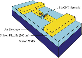
Figure 1 sketches the structure of SWCNT-TFTs used in this study. The TFT consists of two Au electrodes (100 nm thick) patterned on top of the silica substrate and SWCNT networks as active layers. The device active channel is 50 μm long and 50 μm wide. The SiO2 layer of 300 nm thickness serves as the gate dielectric. The silica surface was first treated with 3-aminopropyltriethoxysilane (Sigma-Aldrich) to improve its adhesion with SWCNTs. The concentration of 500-nm long tube suspension was adjusted to 0.02 mg/mL using the 2 wt% DOC solution, while that of the 150-nm long tube suspension was 0.04 mg/mL. Diluted length-sorted SWCNT suspensions were then dropped on treated surface across TFT channels to form active layers. Different volume of SWCNT suspensions were used to produce SWCNT thin films of various densities in the channel, followed by drying at room temperature and rinsing by methanol. For the 500-nm long SWCNT suspension, ∼1.6 μL suspension was needed to form low-density film, while ∼2.2 μL was used to form the optimum-density film. For 150-nm long SWCNT suspension, 2.4 and 3.6 μL suspensions were used to form the low-density and optimum-density films, respectively. TFT performance characterization was carried out in ambient condition using a Keithley semiconductor characterization system (4200-SCS, Cleveland, OH). For each device, currents between source and drain (I d) were measured under a bias voltage (V d) of 2 V, while sweeping the gate voltage (V g) from 40 to −40 V.
A schematic drawing of a thin film transistor using SWCNT networks as its active layer bridging a pair of Au source and drain electrodes.

III. RESULTS AND DISCUSSION
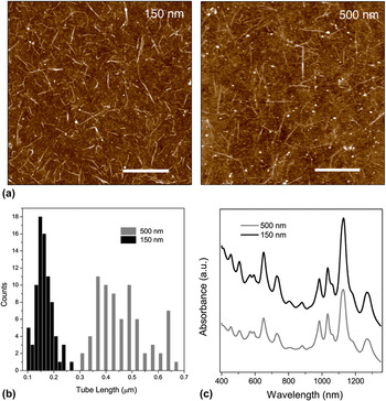
Figure 2(a) shows the typical AFM images of two length-sorted SWCNT samples investigated in this work. They suggest that isolated individual tubes were obtained. The length distribution obtained through AFM image analysis is illustrated in Fig. 2(b). The average tube length of the two samples is 150 ± 33 nm and 500 ± 91 nm, respectively. SWCNT suspensions extracted after length sorting were also characterized by UV–vis–NIR spectrophotometer. Figure 2(c) shows their absorbance spectra, and spectra are shifted in Y-axis for better comparison. Both spectra have almost flat absorption backgrounds, indicating that most carbon impurities in SWCNT samples have been removed in centrifugation and sorting. The well-resolved sharp spectra peaks are from the excitonic optical absorption bands corresponding to the first and second one-dimensional van Hove singularities, which suggest that most of tubes are not in large bundles. The spectral features of both samples are similar, suggesting that the length sorting changes neither the diameter distribution nor the m- to s-SWCNT ratios.
(a) AFM images of two length-sorted SWCNT fractions (left, 150 ± 33 nm; right, 500 ± 91 nm). The size of both the images is 4 × 4 μm with the scale bar of 1 μm. (b) Length distribution histograms of length-sorted SWCNTs measured by analyzing AFM images. (c) UV–vis–NIR absorbance spectra of the two length-sorted SWCNTs. Gray and black lines are data from tubes with the average length of 500 and 150 nm, respectively.

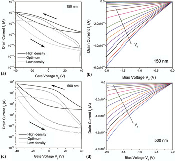
Figure 3 shows the typical transfer characteristics, forward and reverse sweeps of drain current versus gate voltage, and output characteristics, drain current versus bias voltage for SWCNT-TFTs fabricated using 150 ± 33 nm and 500 ± 91 nm tubes, respectively. A p-type behavior and a hysteresis are observed, which have been credited to the p-doping by absorbed O2 moleculesReference Collins, Bradley, Ishigami and Zettl32 and a charge trapping effect,Reference Kim, Javey, Vermesh, Wang, Li and Dai33 respectively. Figures 3(a) and 3(c) show that the density of tubes in device channels significantly changes the on-current, off-current, and on/off ratio. Higher tube density leads to higher on-current and off-current, while smaller on/off ratio. SWCNTs with the two different lengths also behave differently. SWCNT-TFTs fabricated using longer 500 ± 91 nm tubes have higher on-currents. Figures 3(b) and 3(d) suggest that no leakages are detected under our typical testing conditions.
Electrical transport properties of DOC-wrapped SWCNT-TFTs with (a, b) 150- and (c, d) 500-nm tube length. Channel length and width are both 50 μm. (a, c) Transfer characteristics. The source–drain voltage was held at V d = 2 V. (b, d) I d–V d characteristics of the same device. Applied gate voltage (V g) was in the range from 0 (top) to −40 V (bottom) with 2 V steps.

To clarify the effect of tube length on SWCNT-TFT performances, we fabricated SWCNT thin films of different densities by changing the volume of DOC-wrapped SWCNT suspensions used. Eighty and fifty SWCNT-TFTs were fabricated using SWCNTs with the lengths at 150 and 500 nm, respectively. The mobility (μ) of TFTs is calculated by using the equation:
 $$<![CDATA[$${\rm{\mu }}\, = \,{{L_{{\rm{ch}}} } \over {W_{{\rm{ch}}} }} \times {{t_{{\rm{OX}}} } \over {\rm{\varepsilon }}} \times {1 \over {V_{\rm{d}} }} \times {{dI_{\rm{d}} } \over {dV_{\rm{g}} }}\quad,$$
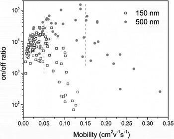
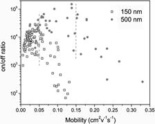
where W ch represents the width of the device channel (50 μm), ε is the dielectric constant of SiO2, L ch is the length of the channel (50 μm), and t OX is the thickness of SiO2 layer (300 nm). Figure 4 shows the correlation between the on/off ratio and mobility of SWCNT-TFTs. Each data point on Fig. 4 represents the characteristics of one device. For SWCNT-TFTs fabricated using 500-nm long tubes, the data points can be divided into two regions by the dashed line on Fig. 4. On the left of the dashed line, the on/off ratio increases dramatically with increasing mobility. TFTs have high on/off ratios ranging from 103 to 105 and the mobility of 0.02–0.15 cm2/(V s). In contrast, on the right of the dashed line, the on/off ratio decreases under increasing mobility. Near to the dashed line, the on/off ratio of TFTs reaches a maximum around 105 with the mobility at ∼0.15 cm2/(V s). For low-density thin films, increasing tube density helps to improve both on/off ratio and mobility. In contrast, when the tube density is too high, large amount of m-SWCNTs would form conducting paths connecting between source and drain electrodes, resulting in lower on/off ratios. Similar trends are observed on SWCNT-TFTs fabricated using 150-nm long tubes shown on Fig. 4. However, the maximum on/off ratio is smaller at around 104, and the mobility marching with the maximum on/off ratio is also much lower at ∼0.05 cm2/(V s). These results suggest that when the SWCNT-TFTs have the maximum on/off ratio, its corresponding SWCNT network density could be considered as an optimum tube density for achieving good SWCNT-TFT performances. The optimum tube density depends on tube length.
Correlation between the on/off ratio and mobility of SWCNT-TFTs at different tube densities. Black squares and gray circles represent results of TFTs fabricated by 150- and 500-nm long SWCNTs, respectively.

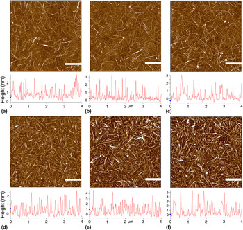
To find out the optimum tube density for the two tested SWCNT samples, AFM was used to characterize SWCNT thin films in TFT channels at three different densities. AFM was used to characterize SWCNT thin films in TFT channels at three different densities. Figure 5 shows SWCNT thin films at high, optimum, and low densities, corresponding to SWCNT-TFTs’ transfer characteristics sketched in Fig. 3. The performance of TFTs using the low-density films [Figs. 5(a) and 5(d)] falls in the area on the left side of the dash lines on Fig. 4, which is just above percolation. The two optimum-density films [Figs. 5(b) and 5(e)] match to TFTs with the maximum on/off ratios at ∼0.15 and ∼0.05 cm2/(V s), respectively. The high-density films [Figs. 5(c) and 5(f)] are those on the right of the dash lines on Fig. 4. The tube densities by analyzing AFM images are listed in Table I. Comparing SWCNTs at the two lengths, the 500-nm long tubes show much lower density compared with that of the 150-nm tubes. The standard percolation theory predicts that the conductivity of an SWCNT thin film depends on the tube density following the correlationReference Hu, Hecht and Gruner13:
 $$<![CDATA[$${\rm{\sigma }}\, \,\propto \,(N - N_{\rm{C}} )^{\rm{\alpha }} \quad,$$
AFM images and height profiles of SWCNT thin films in SWCNT-TFT channels. (a–c) Thin films fabricated by 500-nm long tubes: (a) low density, (b) optimum density, and (c) high density. (d–f) Thin films fabricated by 150-nm long tubes: (d) low density, (e) optimum density, and (f) high density. The size of images is 4 × 4 μm, and the scale bar is at 1 μm.

SWCNT density and bundle size of SWCNT thin films at different densities.

where σ refers to the conductivity in three dimensions or the sheet conductance in two dimensions, N is the density of tubes in the film, NC is the critical density (i.e., the density where the conductivity of the SWCNT thin film changes dramatically), and α is the critical exponent (the theory predicts σ = 1.33 in two dimensions). As reported previously,Reference Pike and Seager34 if considering a SWCNT thin film as an infinite two-dimensional random percolation network, the critical density of tubes can be determined by:
 $$<![CDATA[$$ L({\rm{\pi }}N_{\rm{C}} )^{1/2}\,=\,4.236\quad,$$
where L is the length of SWCNTs. Equations (2) and (3) suggest that shorter tubes need a higher density to reach their percolation threshold. Higher tube density may lead to higher chances of forming conductive paths, which would lower the on/off ratio of transistors. These predictions are consistent with our experimental results shown in Fig. 4. For two SWCNT samples with length of 150 and 500 nm, the theoretical value of N C is 254 and 23 μm2, respectively. AFM images show the low-density films at 92 and 27 μm2, respectively. The difference between theoretical prediction and experimental results, especially for the shorter 150-nm long tubes, can be credited to SWCNT bundling. Height profiles of AFM images show that DOC-wrapped SWCNTs would aggregate into small bundles in TFT channels. The main species in SWCNTs from Co–Mo catalyst is (7, 6) tubes with the diameter of 0.90 nm [see Fig. 2(c)]. For the 500-nm long tubes, in the low-density film, the average height is 1.5 ± 0.5 nm, suggesting that the tube structures seen in AFM are actually small bundles with the diameter of about 1.7 times of individual tubes. In comparison, the low-density 150-nm long tube film has the larger bundle size of 1.8 ± 0.6 nm. With the increase of tube density, the bundle size increases. In the optimum-density films, the bundle diameter increases to 1.7 ± 0.8 nm and 2.4 ± 0.9 nm, respectively. If we estimate tubes are packed together in SWCNT bundles as hexagonal ropes, we could estimate the number of tubes in each bundle. Thus, in the optimum-density film, the actual tube density of the 500-nm long tubes would be around 58 × 3 = 174/μm2, while that of the 150-nm long tubes is about 110 × 7 = 770/μm2. It should be note that the bundles are not all uniform in size, as indicated by the different heights in Fig. 5.
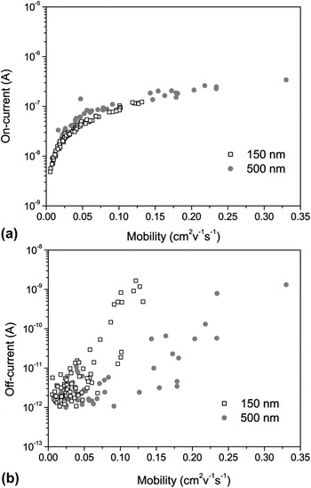
Last, we studied the length dependence in SWCNT-TFTs’ on-current and off-current. Each data point on Fig. 6 represents the characteristics of one device. Figure 6(a) shows the correlation between on-current and mobility. The on-currents increase sharply first with the increase of mobility, which can be credited to the increase of tube density in the SWCNT thin films. The on-current of 500-nm long tube films saturates around 5 × 10⁻⁷ A, while that of the 150-nm long tube films saturates around 1 × 10⁻⁷ A. At the same mobility, the on-currents generated by film comprising longer 500-nm tubes are higher than that from films comprising shorter 150-nm tubes. The higher on-currents of the longer tubes can be credited to fewer tube–tube junctions in SWCNT thin films. In our study, the total mass of SWCNTs in the optimum-density films can be determined based on their density and length. There are 174 and 770 μm2 tubes in the optimum-density films comprising 500- and 150-nm long SWCNTs, respectively. The mass of an individual nanotube is proportional to its length. The total mass ratio of SWCNTs in these two films would be around 0.75 (≈1). There is no significant mass difference for short and long SWCNT-based TFTs. Thus, the observed performance difference does not come from the mass difference of nanotubes in the device channel. The on-currents observed in this study are lower than several previous studies.Reference Asada, Nihey, Ohmori, Shinohara and Saito9–Reference Lee, Weng, Wei, Chen, Chan-Park, Tsai, Leou, Poa, Wang and Li11, Reference Si, Wang, Chen and Chen31, Reference Lee, Han, Chen, Wei, Chen, Chan-Park and Li35 This can be attributed to three reasons: (i) surfactant-wrapped SWCNTs were used in study, while DNA-wrapped SWCNTs were used by some other studies.Reference Asada, Nihey, Ohmori, Shinohara and Saito9, Reference Asada, Miyata, Ohno, Kitaura, Sugai, Mizutani and Shinohara10, Reference Si, Wang, Chen and Chen31 Surfactants, such as DOC, would fully cover the surface of SWCNTs. In contrast, DNA would only partially cover the surface of nanotubes. Surfactant residues may increase the tube–tube contact resistance as compared to the direct tube–tube contacts, resulting in lower on-currents. (ii) We used a device channel length of 50 μm, which is longer than some previous studies.Reference Asada, Miyata, Ohno, Kitaura, Sugai, Mizutani and Shinohara10, Reference Si, Wang, Chen and Chen31 When the channel length is longer, more SWCNTs are required to form conductive paths, resulting in more tube–tube contacts. (iii) The purity of SWCNTs is also different. We have used SWCNTs without specific metallicity separation in this study. SWCNTs enriched with semiconducting nanotubes would achieve better performances.Reference Lee, Weng, Wei, Chen, Chan-Park, Tsai, Leou, Poa, Wang and Li11, Reference Lee, Han, Chen, Wei, Chen, Chan-Park and Li35
Length-dependent correlations between (a) on-current, (b) off-current of SWCNT-TFTs and their mobility.

The correlation between off-current and mobility is presented in Fig. 6(b). At lower mobility, the off-currents from tubes of two different lengths all stay around 10−12 A. At higher mobility, the off-currents increase to about 1.5 × 10⁻⁹ A. Because the diameter distribution and the m- to s-SWCNT ratios of both SWCNT samples are similar, the increase in off-currents can be attributed to the higher percolative conduction through metallic tubes in high-density SWCNT films. Our results of on-current and off-current are consistent with previous findings.Reference Hu, Hecht and Gruner13, Reference Chun, Fagan, Hobbie and Bauer24 When SWCNT length is shorter, higher tube density is needed to form semiconducting paths, which results in a simultaneous increase in the number of SWCNT junctions and conductive pathways.Reference Yang, Kong, Jung, Baek, Han, Oh and Jung6 The former will lower on-current, and the latter probably increases the off-current.
IV. CONCLUSIONS
Two DOC-wrapped SWCNT suspensions with the average tube length of 150 ± 33 nm and 500 ± 91 nm were evaluated in SWCNT-TFTs. TFTs fabricated using 500-nm long tubes have maximum on/off ratio around 105 with the mobility at ∼0.15 cm2/(V s). In contrast, TFTs using 150-nm long tubes have lower maximum on/off ratio at around 104 with the lower mobility at ∼0.05 cm2/(V s). Shorter tubes require higher tube density to form semiconducting paths, leading to lower on/off ratio and high contact resistance. Surfactant-wrapped SWCNTs would also bundle together into small ropes when tube density is increased. Shorter tubes form larger bundles. It is essential to control tube length as well as surfactant residue content to construct high performance SWCNT-TFTs.
ACKNOWLEDGMENTS
This work was supported by National Research Foundation, Singapore (NRF-CRP2-2007-02), and Ministry of Education, Singapore (MOE2011-T2-2-062).