I. INTRODUCTION
After the discovery of the giant magnetoresistance (GMR) effectReference Baibich, Broto, Fert, Van Dau Nguyen, Petroff, Etienne, Greuzet, Friederich and Chazelas1 and its use in high-density magnetic recording mediaReference Parkin, Jiang, Kaiser, Panchula, Roche and Samant2 and novel magnetic sensors,Reference Ktena, Hristoforou and Grimes3, Reference Hristoforou4 the interest for one dimensional and two dimensional magnetic materials showing a significant magnetoresistance (MR) response increased significantly. Recently, single and multilayered ferromagnetic nanowires have been prepared and studied both from the fundamental point of view and concerning their potential applications. Especially for multilayered nanowires, the interest has been boosted after the evidence of the GMR effect for current perpendicular to the plane configuration.Reference Pratt, Lee, Slaughter, Schroeder and Bass5–Reference Piraux, Dubois, Duvail, Ounadjela and Fert7 Another very promising area of applications for multilayered nanowires derives from the pioneering work of BergerReference Berger8 and Slonczewski.Reference Slonczewski9 A spin-polarized current can transfer its angular momentum to a ferromagnet, inducing a torque on its magnetization. Thus, the magnetic moment can switch to another state or oscillate around its equilibrium position at microwave frequencies. These are known as the spin transfer torque (STT) phenomena. The potential applications of these phenomena are in nonvolatile memoriesReference Katine, Albert, Buhrman, Myers and Ralph10, Reference Wegrowe, Hoffer, Guittienne, Fabian, Gravier, Wade and Ansermet11 and high-frequency telecommunications.Reference Kiselev, Sankey, Krivorotov, Emley, Schoelkopf, Buhrman and Ralph12
There are many different ways to produce nanowires, including chemical vapor deposition,Reference Cheng, Zhang, Chen, Li, Zhu, Zhu, Fei and Mao13 vapor–solid–liquid technique,Reference Wu and Yang14 and lithography technique.Reference Contreras, Grunes, Yan, Liddle and Somorjai15 But one of the cheapest ways is the electrochemical deposition.Reference Heydon, Hoon, Farley, Tomlinson, Valera, Attenborough and Schwarzacher16 It is also a fast technique allowing to produce large arrays of identical magnetic entities with large aspect ratios (length divided by diameter), which is not possible with standard lithographic techniques.
For studies on both GMR and STT and their applications, small diameter nanowires are required to allow a large (>107 A/cm2) current density per structure and a higher areal density for device arrays. Also, the smaller the diameter, the weaker is the effect of the Oersted field.Reference Heinen, Boulle, Rousseau, Malinowski, Kläui, Swagten, Koopmans, Ulysse and Faini17 Equally important for the GMR and STT phenomena is to control the magnetic properties of the multilayered nanowires. The overall magnetic properties of these structures will depend significantly on the specific magnetic properties of each of the different magnetic layers of the system and the coupling mechanisms that might occur between the layers and interwires. Multilayered nanowires provide the opportunity to tune their magnetic properties by tailoring different parameters influencing their macroscopic behavior,Reference Sun, Hao, Chien and Searson18 such as the thickness of the ferromagnetic and the nonmagnetic layers, the diameter of the nanowires, the pore density, and the electrochemical bath composition.Reference Li, Seet, Fan and Yi19, Reference Seet, Li, Zhao, Wong, Zheng and Lee20
For better tuning of the magnetic properties of multilayered nanowire arrays, the dipole coupling between the adjacent ferromagnetic layers and also the coupling with the neighboring nanowires must be taken into account.Reference Strijkers, Dalderop, Broeksteeg, Swagten and de Jonge21–Reference Tang, Wang and Shima23 Several models have been developed to interpret and calculate the magnetostatic coupling between single nanowiresReference Encinas-Oropesa, Demand, Piraux, Huynen and Ebels24–Reference Valazquez, Pirota and Vazquez27 and/or between multilayered nanowires.Reference De La Torre Medina, Darques, Blon and Piraux28–Reference Chiriac, Ovari and Pascariu31 It must be noted that Ruderman-Kittel-Kasuya-Yosida (RKKY) interactionsReference Ruderman and Kittel32–Reference Yosida34 do not influence our samples because the thickness of the Cu layer is too large, and thus RKKY mechanism does not have any important contribution.
It is already known that the effective anisotropy field of an array of multilayered nanostructures can be tailored by controlling the aspect ratio of the magnetic and nonmagnetic layers.Reference Tang, Wang and Shima23, Reference De La Torre Medina, Darques, Blon and Piraux28, Reference Chen, Chien and Searson35–Reference Lee, Scholz, Nielsch and Gosele38 To explain this, Medina et al.Reference De La Torre Medina, Darques, Blon and Piraux28 proposes an analytical magnetostatic model for determination of the effective anisotropy field, considering both the influence of the magnetic layer thickness and the dipolar coupling between the layers. The model fits well with the experimental ferromagnetic resonance results for the effective anisotropy field of an array of electrodeposited CoCu/Cu nanowires with the diameter of 140 nm.Reference De La Torre Medina, Darques, Blon and Piraux28
In this work, we investigated the capability to adjust with accuracy the orientation of the magnetization easy axis for arrays of both multilayered NiFe/Cu nanowires with large (200 nm) and small (35 nm) diameters by varying the aspect ratio of the NiFe (from 0.1 to 1.42) and Cu layers (from 0.05 to 0.28). This work is additional to those reported in Refs. Reference Tang, Wang and Shima23, Reference De La Torre Medina, Darques, Blon and Piraux28, and Reference Ruderman and Kittel32 done on CoNi/Cu nanowires with diameter of ~250 nm, Ni/Cu nanowires with diameters of 100 and 50 nm, and CoCu/Cu nanowires with the diameter of 140 nm, respectively. We correlated the magnetic hysteresis loop measurements with the calculations of the effective anisotropy field on the basis of the magnetostatic model proposed in Ref. Reference De La Torre Medina, Darques, Blon and Piraux28 to gain a better insight about the influence of the magnetostatic effects on the modulation of the magnetic properties of an array of multilayered nanowires. Using the results from both the experiments and calculations, we analyzed how the variation of the aspect ratio of the magnetic and nonmagnetic layers alters the shape anisotropy and the magnetostatic coupling and how it can be used to determine the magnetization easy axis direction.
Taking into account the reported models for the investigation of the magnetostatic interactions between nanowires and between the adjacent magnetic layers in single and multilayered nanowires,Reference Encinas-Oropesa, Demand, Piraux, Huynen and Ebels24–Reference Chiriac, Ovari and Pascariu31 we propose two formulas for the calculation of the saturation field, when the external field is applied parallel and perpendicular to the nanowires’ axis. We have tested the validity of the functions by comparing the calculated and the experimental results, and the fitting is pretty well as it will be shown further. Furthermore, the calculations based on these two formulas give the variation of the saturation field of NiFe/Cu multilayered nanowire arrays depending on the thickness of the magnetic and nonmagnetic layers for two different diameters (35 and 200 nm), when the external applied field is parallel with and perpendicular to the nanowires’ axis.
II. EXPERIMENTAL PROCEDURE
The nanowires were grown inside the commercially available AAO templates. The templates have thicknesses of 40 μm and nanopore diameters of 35 and 200 nm, hexagonally arranged. The fluctuation in the diameter of the pores is about 2% for the templates with the nanopores of 35 nm and 5% for those with the nanopores of 200 nm.
The nanopores of the AAO templates were filled completely with Ni79Fe21/Cu (noted from now on as NiFe/Cu) by pulsed electrodeposition.Reference Nielsch, Müller, Li and Gösele39 The multilayered nanowires were fabricated at room temperature by using an aqueous solution of 90 g/L NiSO4, 13.5 g/L FeSO4, 2 g/L CuSO4, and 25 g/L H3BO3.Reference Chiriac, Dragos, Grigoras, Ababei and Lupu40 The pH value of the electrolyte was adjusted at 3 by adding a few drops of either 0.5M H2SO4 solution or 1M NaOH solution. Because the deposition potential of Cu is much less negative than that of NiFe, the multilayered nanowires were prepared by switching between the deposition potentials of Cu and NiFe. The electrochemical deposition was carried out in a three-electrode cell,Reference Chiriac, Dragos, Grigoras, Ababei and Lupu40 at constant voltage of −1.4 V for NiFe alloy and −0.5 V for Cu. A thin layer of Au and Cr was deposited by e-beam evaporation on one side of the AAO template, serving as working electrode for subsequent electrodeposition. A three-electrode cell with a platinum wire as counter electrode and an Ag/AgCl as reference electrode were used to carry out the electrodeposition process. The applied voltage was controlled during the electrodeposition with a HEKA PG 340 bipotentiostat/galvanostat.
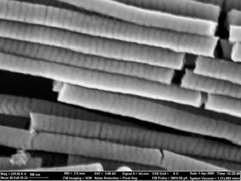
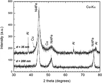
For compositional energy-dispersive spectroscopy (EDS) analysis, the AAO template was dissolved in a KOH 3M aqueous solution, and the free nanowires were separated from the hydroxide solution using a permanent magnet and rinsed several times with distilled water. The scanning electron microscope/EDS analysis (Carl Zeiss Neon 40EsB CrossBeam) confirmed the formation of NiFe/Cu multilayered structures (Fig. 1), with the composition of NiFe in the range Ni79 ± 2Fe21 ± 2. The presence of Ni4Fe (permalloy-like structure) and Cu distinct layers is proved also by the x-ray diffraction pattern shown in Fig. 2.
Scanning electron microscope image of [NiFe (50 nm)/Cu (10 nm)] × n electrodeposited multilayered nanowires.

X-ray diffraction patterns of [NiFe (50 nm)/Cu (10 nm)] × n electrodeposited multilayered nanowires with d = 35 nm and d = 200 nm, respectively.

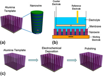
Figure 3 presents the sequence of steps needed for the fabrication of NiFe/Cu multilayered nanowires [Fig. 3(b)] and the process that follows to prepare the template with the nanowires in it for structural and magnetic measurements [Fig. 3(c)]. During the last step of the procedure [Fig. 3(c)], the system AAO template-electrodeposited nanowires is mechanically polished (Kent MK 2A, Engis Ltd.) using diamond (particles size ~3 μm) and Syton (particles size ~20 nm) solutions to remove the thin metallic layer formed on the top of the membrane. This layer acts magnetically different compared with the nanowires, influencing the total magnetic behavior of the sample, and it is important to be removed for the accuracy of the magnetic measurements. By polishing, all nanowires are brought to the same length of 20 μm and further used for experimental investigations.
(a) Schematic representation of a small region of a template and a nanowire grown inside a pore; (b) illustration of the electrochemical deposition technique; (c) the steps followed from the fabrication until the measurements of the nanowires.

The magnetization hysteresis loops of multilayered nanowires were measured at room temperature using a LakeShore Vibrating Sample Magnetometer (VSM), model 7410. The M–H curves were recorded with the magnetic field applied parallel with the nanowires’ axis (H //) (perpendicular to the template plane) and perpendicular on the nanowires’ axis (H ┴) (parallel with the template plane) and swept between ±800 kA/m.
III. THEORETICAL APPROACH
The orientation of the magnetization easy axis for an array of multilayered nanowires is determined by a competition between the shape anisotropy, magnetocrystalline anisotropy, magneto-elastic anisotropy, and magnetostatic coupling between the adjacent ferromagnetic layers and also the magnetostatic coupling between the neighboring nanowires. For permalloy (Py = NiFe), the influence of the magnetocrystalline anisotropy is negligibleReference Chiriac, Dragos, Grigoras, Ababei and Lupu40 and thus will be excluded from the calculations.
H eff is the effective anisotropy field, which in its general form, for isolated particles, contains contributions from the shape, magnetocrystalline, and/or magneto-elastic anisotropy. As it was shown, for electrodeposited Ni nanowires in polycarbonate membranes, the contribution from the magneto-elastic anisotropy at room temperature is negligible.Reference Dubois, Colin, Duvail and Piraux41 Additionally, as it was mentioned in the previous paragraph, for permalloy layers, the magnetocrystalline anisotropy is also negligible. Therefore, the effective anisotropy field becomes purely magnetostatic and can be written as a function of the demagnetizing factors N ⊥ and N ∥:

H eff defines whether the magnetostatic anisotropy favors an easy axis direction parallel or perpendicular to the nanowires’ axis. N ∥ and N ⊥ are the demagnetizing factors parallel and perpendicular on the nanowires’ axis, M s being the saturation magnetization. For N ⊥ > N ∥, H eff > 0, thus the magnetostatic anisotropy favors an easy axis parallel with the nanowires’ axis, whereas for N ⊥ < N ∥, H eff < 0, favoring an easy axis perpendicular to the nanowires’ axis.
For rod-shaped samples (like the nanowires), the demagnetizing factors N ∥ and N ⊥ are connected by the relationReference Sun, Hao, Chien and Searson18

Therefore, Eq. (1) can be written as

For isolated permalloy layers, awareness of N ∥ or N ⊥ is enough to have a good indication for the direction of the magnetization easy axis. But this is not the case for multilayered nanowires, where the dipole–dipole interactions must be taken into account as they have strong influence on the preferred orientation of the easy axis.
For isolated multilayered nanowires with a large and finite number n of magnetic layers, according to Ref. Reference De La Torre Medina, Darques, Blon and Piraux28, the dipolar interactions along the direction of the nanowires’ axis can be expressed as a finite monotone alternating sum of demagnetizing fields, H i. H i is the magnetostatic field created by the internal layers of each pair of interfaces. Therefore, the total demagnetizing factor on the direction along the axis of the multilayered nanowires, N ∥tot, can also be expressed as an alternating sum of demagnetizing factors, N i, which corresponds to each demagnetizing field H i. Replacing in Eq. (3) the demagnetizing factor of a single layer with the total demagnetizing factor along the axis of a multilayered nanowire N ∥tot, H eff of an isolated multilayered nanowire can be calculated by taking into account the magnetostatic coupling between the adjacent layers. Additionally, in Ref. Reference De La Torre Medina, Darques, Blon and Piraux28, proceeding one step further, in the equation for H eff is incorporated the influence of the magnetostatic coupling between neighboring nanowires in arrays of single nanowires:

where P is the porosity or filling factor, defined as the product of the areal pore density by the pore surface.Reference Lee, Ji, Gosele and Nielsch42
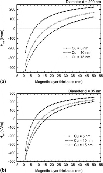
Figure 4 presents the variation of the effective field, H eff, as a function of the NiFe magnetic layer thickness for multilayered nanowires with diameters of (a) 200 nm and (b) 35 nm, and for three different Cu layer thicknesses of 5, 10, and 15 nm. The effective anisotropy field values have been calculated by using Eq. (4). By decreasing the thickness of the NiFe ferromagnetic layer, H eff is decreased. This is due to the decreasing aspect ratio, leading to an increase of N ∥tot and consequently the decrease of N ⊥tot. As a result, the difference between N ⊥tot and N ∥tot reduces and the applied field required to change the magnetization direction from the easy to the hard axis is decreasing. For a critical thickness of the NiFe magnetic layer, which depends on the nanowire diameter and the thickness of the Cu nonmagnetic layer (the critical thickness is larger for larger diameters and thicker Cu layers), H eff changes the sign from positive to negative, and the easy magnetization axis is not any more the axis parallel with the nanowires, but perpendicular to them. The magnetic layer critical thickness that works as threshold for the change of orientation of the magnetization is not steady. It strongly depends on the thickness of the nonmagnetic layer, which controls the intensity of the dipole–dipole coupling between the adjacent ferromagnetic layers, and the pore density. Thinner spacer layers result in stronger coupling between the magnetic segments, which favors the magnetization orientation parallel with the nanowires’ axis.
H eff for multilayered nanowires’ arrays, as a function of the thickness of the NiFe layer, for three different Cu spacer layer thicknesses: (a) nanowires with d = 200 nm and (b) nanowires with d = 35 nm.

The saturation field, H sat, i.e., the field needed to align the magnetic moments along the field direction, for an isolated nanowire is determined by the intrinsic magnetic properties. As it was mentioned before, for NiFe nanowires at room temperature, the magnetocrystalline and magneto-elastic anisotropy are negligible. Therefore, H sat, must overcome only the demagnetizing field. Knowing the demagnetizing factor, N ∥, of a single nanowire, the saturation field can be calculated by using the equation

For a multilayered nanowire, we include the magnetostatic coupling between the ferromagnetic layers into this equation by substituting the demagnetizing factor N ∥ with the total demagnetizing factor, N ∥tot. Then Eq. (5) gives the field that should be applied to overcome the total demagnetizing field along the axis of a multilayered nanowire. Additionally, from Eqs. (2) and (5), by substituting N ∥tot with N ⊥tot, we can also calculate the field that must be applied perpendicular to a multilayered nanowire to achieve saturation.
Furthermore, to calculate H sat for multilayered nanowire arrays, the magnetostatic influence from the neighboring nanowires must be included in Eq. (5). For that we must take into consideration two different cases because the dipole coupling between nanowires in the template depends on the direction of the external applied magnetic field.
A. External field applied parallel with the nanowires’ axis
When the external field is applied parallel with the nanowire axis, the influence of the dipolar coupling between the nanowires is expressed by an additional uniaxial anisotropy field, H U,Reference Encinas-Oropesa, Demand, Piraux, Huynen and Ebels24 which favors an easy axis perpendicular to the nanowires. The saturation field is then

As reported by Encinas et al.,Reference Encinas-Oropesa, Demand, Piraux, Huynen and Ebels24 by using a phenomenological mean field approach, the contribution of the neighboring nanowires on the dipolar coupling depends on the porosity, P, of the template. Upon decreasing the nanowire separation (increasing P), the nanowires start to interact via their dipolar stray fields. Therefore, besides the self-demagnetizing field, there will be two additional contributions that are taken proportional to P. First, the charges on the cylindrical nanowires’ surface produce a dipolar field that opposes the self demagnetization field and can be expressed as 2πM sP. Second, the charges at the top and bottom extremities give rise to an interaction field expressed as 4πM sP. Combining the two field contributions in Eq. (5), the net magnetostatic field yields

The reason for using plus sign instead of minus in Eq. (7) is that the dipolar field acts antiparallel to the orientation of the saturation magnetization and consequently opposes it. Therefore, additional field must be applied to saturate the multilayered nanowires’ array.Reference Sampaio, Sinnecker, Cernicchiaro, Knobel, Vazquez and Velazquez22
B. External field applied perpendicular to the nanowires’ axis
For an external field applied perpendicular to the nanowires’ axis, the dipole–dipole interaction between nanowires can be approximately calculated using the formula given by Zhan et al.,Reference Zhan, Gao, Liang, Di and Cheng25 which combines the dipolar approximation with a length correction in arrays of individual nanowires:

where d is the pore diameter and d int is the interpore distance (from center to center). For the multilayered nanowires with the demagnetizing factor N ⊥tot, the saturation field for the array is given by the function:

Contrary to the case of the applied field parallel with the nanowires’ axis, now the magnetostatic dipolar coupling between neighboring nanowires acts parallel to the orientation of the saturation magnetization. As a result, less external field is needed to saturate the array of multilayered nanowires and that explains the “minus” sign in Eq. (9).
IV. RESULTS AND DISCUSSION
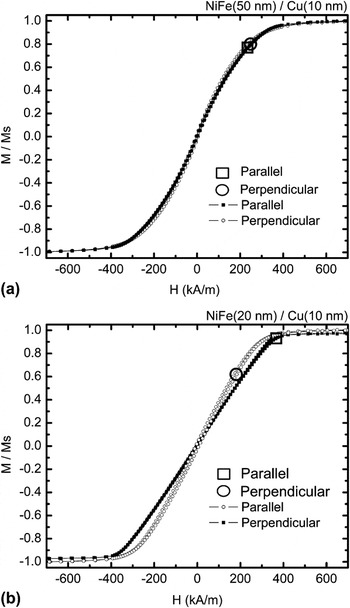
Figure 5 presents the VSM measurements for the nanowires with d = 200 nm. The first sample has NiFe layers of 50-nm thickness and Cu layers of 10-nm thickness [Fig. 5(a)]. For isolated permalloy layers with the thickness of 50 nm and diameter of 200 nm, N ∥ > N ⊥ (all the calculations of N ⊥ and N ∥ in this article are based on the functions given in Ref. Reference Sun, Hao, Chien and Searson18), thus H eff < 0 and the easy magnetization axis is perpendicular to the cylinder axis. Contrary to the calculations for isolated permalloy layers, for an array of multilayered nanowires with NiFe layers of 50-nm thickness and 200-nm diameter, the VSM measurements show that the magnetization curves are essentially identical for applied field perpendicular and parallel to the nanowires’ axis. This can be interpreted mainly by the strong influence of the dipolar coupling between the ferromagnetic layers of each nanowire, which has the tendency to align the easy magnetization axis along the axis of the nanowires.
Experimental hysteresis loops (normalized) of NiFe/Cu multilayered nanowires with diameters of 200 nm, for applied field parallel and perpendicular to the nanowire axes: (a) for 50-nm thick NiFe and 10-nm thick Cu and (b) for 20-nm NiFe and 10-nm Cu. The calculated values of the saturation field, H sat, for applied field parallel and perpendicular to the nanowire axis are also shown for comparison.

The demagnetizing factor along the axis of an isolated cylinder with the diameter of 200 nm and thickness of 50 nm is N ∥ = 0.70. Taking into account the dipole coupling between the ferromagnetic layers, the total demagnetizing factor along the axis of the wire N ∥tot= 0.14 (all the calculations of N ∥tot in this article are based on the function given in Ref. Reference De La Torre Medina, Darques, Blon and Piraux28), which is much smaller than that for an isolated cylinder. From Eq. (2) N ⊥tot = 0.45. As N ∥tot > N ⊥tot, there must be a preference for the magnetization to lie along the axis of the nanowires. VSM measurements do not fully overlap with the calculated result, not only because of the variation in the thickness of the Cu layers (10 ± 6 nm) and the NiFe (50 ± 3 nm and 20 ± 2 nm) layers but also because of the slight variation of the nanopore diameter. That can be further understood from the calculation of the saturation field. If there is no variation in the thickness of the Cu and NiFe layers, then N ∥tot = 0.14, and Eq. (7) will give H sat = 234 kA/m. But, if, for example, the Cu layer is 6-nm thicker than what was supposed to be obtained experimentally (i.e., 16 nm instead of 10 nm), then N ∥tot = 0.22, i.e., a larger value, because for thicker spacer layers the coupling is less strong. In these conditions, from Eq. (7) the saturation field is 308 kA/m, closer to the value obtained from the VSM measurements.
For the applied field perpendicular to the nanowires’ axis, the saturation field can be calculated from Eq. (9). The calculated demagnetizing factor N ⊥tot is 0.43. Therefore, from Eq. (9), Hsat = 345 kA/m. However, when we calculated this value, we did not take into account the magnetostatic coupling from the neighboring nanowires. By considering also the influence from the neighboring nanowires, we get a saturation field, H sat = 261 kA/m.
For the second array of multilayered nanowires with the diameter d = 200 nm [Fig. 5(b)], the thickness of the ferromagnetic material is decreased to 20 nm, whereas the thickness of the spacer layer remains the same. From the VSM measurements, the saturation field perpendicular to the nanowires’ axis is smaller than that corresponding to the direction along the axis, indicating that the magnetic easy axis lies in the direction perpendicular to the nanowires. From Fig. 4(a), for a Cu spacer layer of 10 nm, the NiFe ferromagnetic layer must be thinner than 16–17 nm to have preferred orientation perpendicular to the nanowires’ axis. In our case, this condition is achieved for a permalloy layer of ∼20-nm thickness, which is very close to the calculated value. As there is a preferred orientation of the magnetization perpendicular to the nanowire axis, one would expect also large remanence and high coercivity for this orientation. That is not observed on the experimental curves because, for multilayered nanowires with magnetic layers formed in a disk shape, as in our case, the dipole–dipole interactions between adjacent magnetic layers tend to induce an antiparallel alignment of magnetization oriented perpendicular to the nanowires’ axis. For zero applied fields, the adjacent ferromagnetic layers are oriented antiparallel, leading to zero remanence and coercivity.
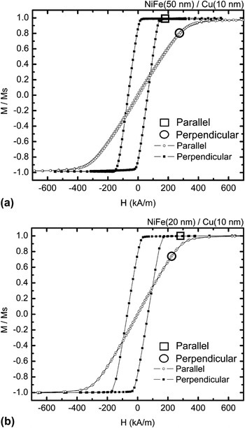
Figure 6 presents the VSM measurements for arrays of multilayered nanowires with the diameter of 35 nm. The measurements are for two combinations of multilayers: NiFe (50 nm)/Cu (10 nm) [Fig. 6(a)] and NiFe (20 nm)/Cu (10 nm) [Fig. 6(b)] multilayered nanowires. The demagnetizing factor along the axis for an isolated cylindrical layer with the diameter of 35 nm and the thickness of 50 nm is N ∥ = 0.24. For the multilayered nanowires with NiFe layers of 50 nm and Cu layers of 10 nm, the total demagnetizing factor along the axis of the wire is N ∥tot = 0.074, and from Eq. (2) N ⊥tot = 0.46. Thus, N ⊥tot > N ∥tot; therefore, the easy magnetization axis is along the wire axis. This is confirmed by the VSM measurements because, for applied fields parallel with the nanowires’ axis, both the coercive field and remanence are large.
Experimental hysteresis loops (normalized) of NiFe/Cu multilayer nanowires with diameters of 35 nm, for applied field parallel and perpendicular to the nanowire axes: (a) for 50-nm thick NiFe and 10-nm thick Cu and (b) for 20-nm thick NiFe and 10-nm thick Cu. The calculated values of the saturation field, H sat, for applied field parallel and perpendicular to the nanowires’ axis are also shown for comparison.

Furthermore, the saturation field, H sat, when the applied field is parallel with the nanowires’ axis is smaller than when the applied field is perpendicular to the wire axis. From Eq. (7), the calculated saturation field in an external field applied parallel with the nanowires is H sat = 179 kA/m, which is approximately the same as the experimental value. For the case of an applied field perpendicular to the nanowires’ axis, for N ⊥tot= 0.46, Eq. (9) will give a saturation field of 282 kA/m. According with Eq. (9), a decrease of the thickness of the Cu spacer layer will lead to higher N ⊥tot and thus higher saturation fields.
Figure 6(b) shows the measured hysteresis loops for the multilayered nanowires with 20 nm NiFe and 10 nm Cu layers. Because the NiFe layer is thinner than before, the total demagnetizing factor along the axis of the nanowire will increase, leading to higher saturation fields for this direction. For the orientation perpendicular to the nanowires’ axis, the total demagnetizing factor will decrease, leading to smaller saturation fields compared with the similar diameter multilayered nanowires with 50-nm thick NiFe layers. That is exactly what we get from the VSM measurements. Additionally, N ∥tot = 0.22 < N ⊥tot = 0.39, indicating a preferred magnetization direction along the axis of the nanowires, which agrees with the experimental results. According to Fig. 4(b), the NiFe magnetic layers should be below 11–12 nm to achieve magnetization easy axis perpendicular to the nanowires’ axis. That explains the inability to succeed experimentally inducing perpendicular orientation for the easy magnetization axis even for a 20-nm thick NiFe layer.
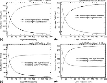
To further investigate the influence of the geometrical characteristics of the magnetic and nonmagnetic layers on the saturation field, we have calculated the variation of the saturation field on the thickness of the magnetic NiFe and nonmagnetic Cu layers for applied fields parallel [calculations are based on Eq. (7)]and perpendicular [calculations are based on Eq. (9)] to the multilayered nanowires’ axis. Calculations were done for multilayered nanowires with diameters of 200 nm [Figs. 7(a) and 7(b)] and 35 nm [Figs. 7(c) and 7(d)].
The calculated saturation field, H sat, as a function of the thickness of the Cu layer (open circles) and NiFe layer (solid squares), for multilayered nanowires with diameters of 200 and 35 nm, respectively: for d = 200 nm and applied field (a) parallel and (b) perpendicular to the nanowires’ axis; for d = 35 nm and applied field (c) parallel and (d) perpendicular to the nanowires’ axis.

As one can see in Fig. 7(a) for the multilayered nanowires with the diameter d = 200 nm and NiFe layer thickness of 15 nm, as the thickness of the Cu layer increases (open circles), the coupling between the magnetic segments weakens, leading to a preferred orientation perpendicular to the nanowires’ axis. As a result, to saturate the nanowires parallel to their axis, stronger fields must be applied, leading to the increase of the saturation field. When the thickness of the permalloy layer varies, while Cu layer is 15 nm, the behavior is vice versa. On increasing the thickness of the NiFe layer, the aspect ratio increases, thus the magnetization easy axis changes the preferred orientation from perpendicular to parallel with the nanowires’ axis. Therefore, it becomes easier to saturate the nanowires along their axis, and less intense field is needed to achieve that.
Figure 7(b) is for the same nanowires diameter, but the applied field is perpendicular to the nanowires’ axis. This time the influence of the thickness of the Cu layer on the saturation field is opposite compared with the case shown in Fig. 7(a). As the thickness of the Cu layer increases, the coupling between the magnetic segments weakens, leading to a preferred orientation perpendicular to the nanowires’ axis. It is easier to saturate the nanowires on this direction, and the saturation field needed is decreasing. When the thickness of the NiFe magnetic layer increases (solid squares), the aspect ratio increases and leads to a preferred orientation of the magnetization parallel with the nanowires’ axis. As a result, the saturation for the direction perpendicular to the nanowires’ axis requires larger applied fields.
A similar behavior was obtained for multilayered nanowires with the diameter of 35 nm [Figs. 7(c) and 7(d)]. The open circles are for the multilayered nanowires with fixed NiFe layer thickness at 10 nm, while the solid squares are for the case when the Cu layer is fixed to 15 nm.
The pretty good agreement between the calculated and experimental results both for the effective anisotropy field and saturation field values confirms the very complex mechanisms that govern the macroscopic magnetic behavior of the multilayered nanowire arrays. The magnetotransport properties reported earlierReference Piraux, Dubois, Duvail, Ounadjela and Fert7, Reference Chiriac, Dragos, Grigoras, Ababei and Lupu40 confirm such a complex behavior of the NiFe/Cu multilayered nanowire arrays, depending on the dimensional characteristics of both nanowires and layers composing the multilayered nanowires. The MR ratio can reach values up to 2–2.5% depending on the thickness of the nonmagnetic Cu layer,Reference Chiriac, Dragos, Grigoras, Ababei and Lupu40, Reference Krimpalis, Dragos, Grigoras, Lupu and Chiriac43 these values being higher than the 0.5–1% values reported for electrodeposited NiFe nanowires.Reference Piraux, Dubois, Duvail, Ounadjela and Fert7, Reference Rheem, Yoo, Koo, Beyermann and Myung44 This increase can be explained by the spin-dependent scattering of the conducting electrons at the sequential ferromagnetic layers composing the multilayered nanowires, this phenomenon being absent in single NiFe nanowires.
V. CONCLUSIONS
The magnetic behavior of arrays of NiFe/Cu multilayered nanowires electrodeposited in AAO templates with nanopore diameters of 200 and 35 nm, respectively, has been investigated. VSM results show that the shape anisotropy and the magnetostatic coupling between adjacent ferromagnetic layers have strong influence on the magnetic behavior of multilayered nanowires’ arrays. The calculated H eff and H sat values fit well with the measured results and prove that the magnetization orientation can be predicted with high accuracy. The calculated diagrams for the effective anisotropy fields, H eff, for different thicknesses of NiFe magnetic and Cu nonmagnetic layers can be used as a guide for the geometrical characteristics that multilayered nanowires must dispose to accomplish the desirable magnetization orientation. Two functions were proposed for calculating the saturation field, H sat, of multilayered nanowire arrays when the applied field is parallel and perpendicular to the nanowires’ axis, respectively. These functions incorporate both the magnetostatic coupling between the adjacent layers of each nanowire and the magnetostatic coupling between the neighboring nanowires.
ACKNOWLEDGMENTS
This work was supported by the European Community under the Sixth Framework Program for the Marie Curie Research Training Network “SPINSWITCH,” Contract No. MRTN-CT-2006-035327.