Introduction
Inkjet printing is a relatively new and promising technology for fabrication; its major advantages, compared with traditional photolithography, rely on fabrication costs reduction, reduced material waste, and simpler manufacturing steps. It is a drop on demand non-contact process, with a large variety of printable substrates and the capacity to reproduce fine features (30 μm maximum resolution).[Reference Stringer, Althagathi, Tse, Duong Ta, Shephard, Esenturk, Connaughton, Wasley, Li, Kay and Smith1] This technology has gained increasing interest in the fabrication of thin films for flexible and stretchable electronics using new functional nanomaterial inks. This technique allows for the manufacturing of devices such as transistors,[Reference Sowade, Ramon, Yoti Mitra, Martínez-Domingo, Pedró, Pallarès, Loffredo, Villani, Gomes, Terés and Baumann2] flexible antenna,[Reference Correia, Mitra, Castro, Rocha, Sowade, Baumann and Lanceros-Mendez3] strain sensors,[Reference Borghetti, Serpelloni, Sardini and Pandini4] and electrochemical biosensors.[Reference Islam Khan, Maddaus and Song5] Despite these established advantages the reliability of both the fabrication process and the fabricated material systems is still a key point to achieve competitive devices.
Moreover, bendable and stretchable electronics require reliable electromechanical interconnects as they are subject to mechanical loading which jeopardizes the integrity of the material itself (the electrical interconnects) or that of the interfaces. A well-established strategy to minimize strains in metal interconnects is in-plane serpentine.[Reference Gonzalez, Axisa, Vanden Bulcke, Brosteaux, Vandevelde and Vanfleteren6] Inkjet printing is a suitable choice for the fabrication of this type of deformable interconnections due to the capability to print a wider range of geometries compared with other printing techniques.[Reference Khan, Lorenzelli and Dahiya7] However, in order to guarantee a successful fabrication of a deformable interconnects, two different aspects should be taken into account. Firstly, the reliability of the process itself, which would answer to the questions of how it is possible optimizing the fabrication process in order to obtain repeatable results. Secondly, the reliability of the inkjet printed device. That is to say, to manufacture devices that guarantee correct functionality under working conditions, i.e., under strain. This reliability can be checked through a proper electromechanical characterization of the printed device.
Printing of silver nanoparticle interconnects on polymer substrata is a widely developed area; however, a thorough investigation of the process parameters and their effect on the electromechanical performances of the printed devices is still lacking. Our work is to assess the electromechanical reliability of metal interconnects on polyethylene terephthalate (PET) and polydimethylsiloxane (PDMS) substrates obtained through different printing conditions using the Dimatix printer. The repeatability of the printing process itself is also subject of this study. In particular, in this paper, process parameters like printing direction, drop spacing, geometrical features, and number of nozzles, have been taken into consideration. To this purpose, conductive linear and serpentine-shaped interconnects obtained using different printing conditions on both substrate types were produced. The interconnects were subjected to electromechanical characterization, coupled with an in-situ optical observation, with the purpose to assess the effect of the geometry of the printed device and of the printing direction only for samples produced with selected processing parameters. The selected parameters were chosen as those that guarantee high quality printed interconnects. The criterion of quality was defined as the processing parameters that ensure the lowest number of defects, in terms of voids and bulges, of the printed pattern, guarantying higher mechanical reliability, and the highest electrical conductance that can be reached, guaranteeing higher electrical performance. Therefore, an accurate evaluation of the substrate wettability, ink adhesion, sintering temperature/time pair, and printing parameters, such as platen temperature, drop spacing, printing direction, and frequency, were performed in order to guarantee an optimal printing.
Compared with PET substrate, PDMS substrate generally requires more substantial changes to the device fabrication process. While the fabrication of stretchable electronics with the traditional photolithography is a well-established area, inkjet printed stretchable interconnections is an emerging topic with an ever-increasing number of papers in the literature, see for example Cheng et al.[Reference Cheng, Wu, Shen, Lai and Huang8] and Jiang et al.[Reference Jiang, Bao, Li, Sun, Zhang, Li, Li, Yao and Song9] This draws attention to the reliability of the fabrication process itself and the materials used. Direct printing of conductive solutions on PDMS is challenging due to its elastomeric, hydrophobic surface, and intrinsic inert behavior. In order to overcome this issue physical approaches, such as UV ozone or oxygen plasma treatments are used. Hence Kim et al.[Reference Kim, Ren, Kim and Noh10] and Abu-Khalaf et al.[Reference Abu-Khalaf, Saraireh, Eisa and Al-Halhouli11] proved that plasma treatment is an effective way to make direct inkjet printing on PDMS substrate possible. However, this process should be finely-tuned because it may induce, as inherent consequence, the embrittlement of PDMS, which makes the treated surface stiffer than the pristine counterpart.[Reference Bowden, Huck, Paul and Whitesides12] Moreover, if the embrittlement is a permanent condition, surface activation is short-lived as hydrophobic recovery is observed within hours. Inkjet printing is an intrinsically slow fabrication process, especially when high quality is required. Therefore, the printing time could be longer than the hydrophobic recovery time, thus affecting the quality (in terms of line width and thickness) of the printed pattern and, in the worst scenario, the printing capability of the surface that recovers the original wettability during printing. This issue leads to search for low-cost, simple, and reliable alternative methods to fabricate interconnects on PDMS substrate. Transfer printing is a widely used fabrication method in the field of stretchable printed electronics[Reference Guo and DeWeerth13, Reference Aziz, Go Bum, Jin Yang, Yang, Kang, Hoi Doh, Hyun Choi and Chan Kim14] that provides an effective route for processing stretchable conductive composites (silver nanowires or carbon nanotubes percolation matrix), but with limited means of producing arbitrary patterns.[Reference Amjadi, Pichitpajongkit, Lee, Ryu and Park15] Instead of direct printing, the conductive material is deposited, usually by means of spin coating, on a donor substrate and then transferred on PDMS through the in-situ polymerization of the elastomeric polymer itself. Therefore, this method ensures strong adhesion between the conductive material and the substrate without any surface treatment. Hence, here the first attempt to use transfer printing method combined with inkjet printing silver nanoparticles ink in order to fabricate printed stretchable interconnects is shown.
Experimental section
Research inkjet printer, Dimatix DMP-2850 (Fujifilm) and commercial silver nanoparticles ink (AgNPs) (Silverjet DGP-40LT-15C, Advanced Nano Products) were used to fabricate interconnects on both PDMS and PET.
As concern the samples on PET substrate a thin PET film (GoodFellow, 23 µm thickness) was used. After the cleaning procedure the substrate was treated with an alkaline etching process. The surface treatment was carried out dipping the thin PET sheet in a 3 M Sodium Hydroxide solution (NaOH, Merck) for 30 min at 60 °C. The surface characterization was performed through contact angle analysis (Drop Shape Analysis software), using DI water as a reference value; furthermore, roughness measures were performed by means of Atomic Force Microscopy (AFM, NT-MDT Solver Pro-M).
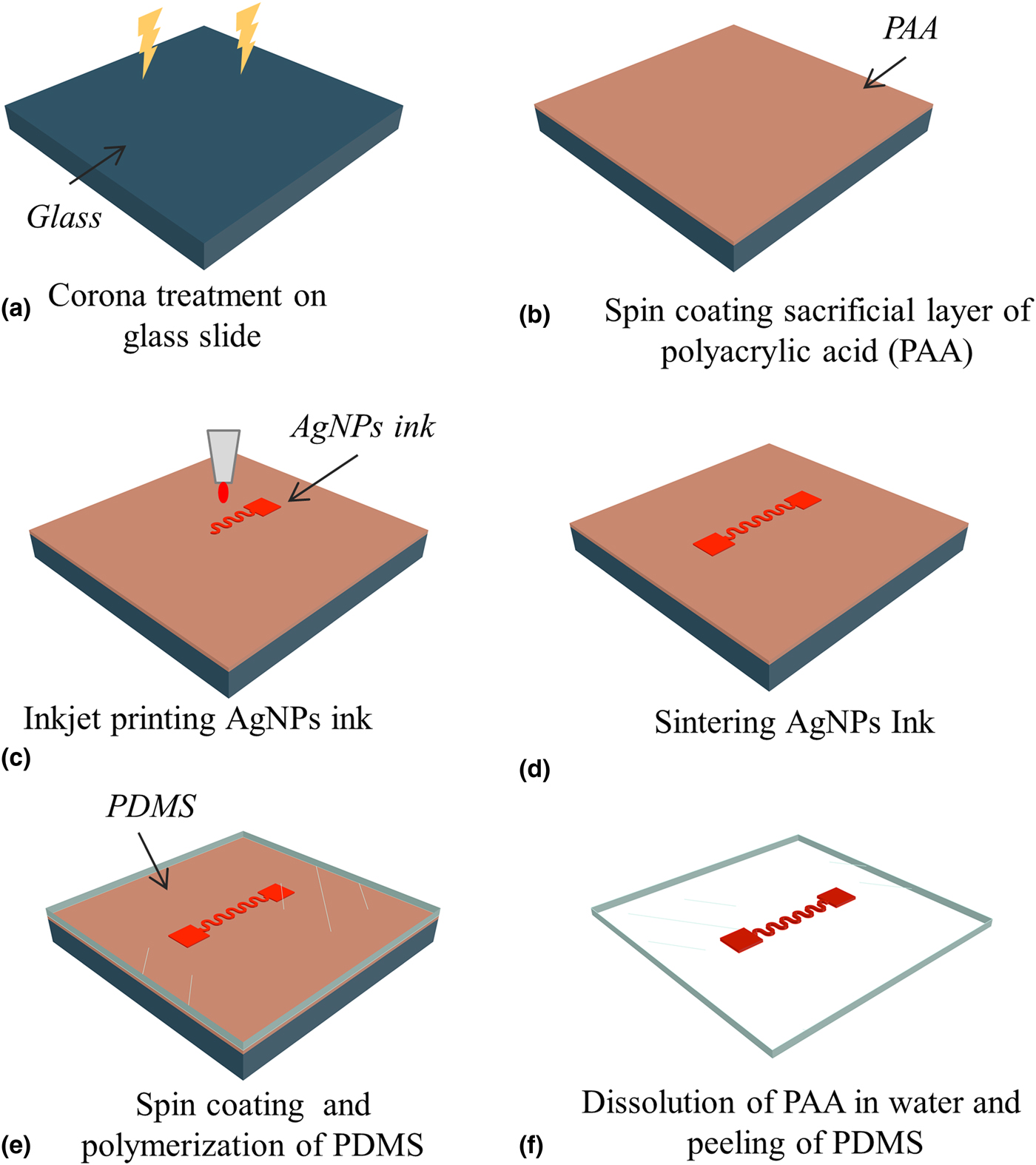
A schematic representation of the proposed transfer printing method for the fabrication of interconnects on PDMS (Sylgard 184, Dow Corning) is shown in Fig. 1. After the cleaning procedure the glass substrate was treated with Corona (BD-20AC) for 1 min in order to increase its wettability. A 17.5 wt% poly (acrylic acid sodium salt) (PAA, Merck) solution was spin coated (Laurell H6-23) on the glass surface at 1000 rpm and dried at 60 °C for 2 min.
Schematic representation of the fabrication process used to realize inkjet printed interconnects on PDMS substrate. (a) Corona treatment on surface of the carrier substrate; (b) Spin coating PAA sacrificial layer; (c) Inkjet printing of AgNPs ink; (d) Sintering of AgNPs ink; (e) Spin coating of PDMS and its polymerization; (f) Dissolution of the sacrificial layer in water and peeling of PDMS. Silver interconnect is transferred on PDMS.

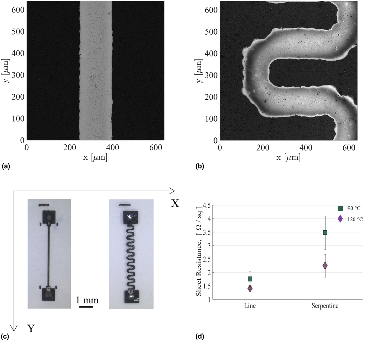
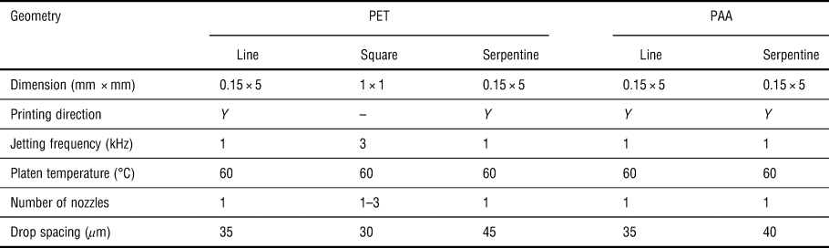
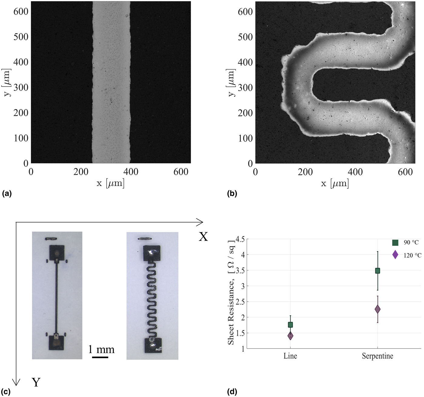
Two different geometries, linear and serpentine interconnects, Figs. 2(a) and 2(b), were directly printed on the PET surface and on the PAA sacrificial layer for the PDMS samples. Table I shows the printing parameters used to print the two patterns by means of a 16-nozzle printhead (Fujifilm Dimatix DMC- 11,610) with a nominal droplet volume of 10 pl for both substrates. The printed interconnects were then sintered at 120 °C for 3 h. Electrical and morphological characterization of the printed interconnects were performed by two-point probing using a Fluke digital multimeter, and by means of Confocal Laser Microscope (CLM, OLS 4100 Olympus). The microscopy analyses were aimed at estimating the integrity of the AgNPs sintered material and their failing mechanism when stretched.
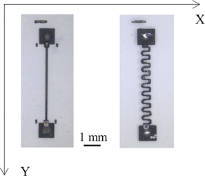
CLM intensity maps of the printed (a) line and (b) serpentine interconnects on PET substrate. (c) Optical images of the inkjet printed interconnects, (left) line and (right) serpentine. Interconnects were printed in Y direction, placing their long axis along Y-axis. (d) Sheet resistance, a figure of merit independent of the specific geometry, at same curing temperature/time for linear and serpentine interconnects.
Print parameters used in order to fabricate serpentine and linear interconnects and squared testing pad on both PET and PAA substrates.

As concern PDMS interconnects, Fig. 1, after the sintering process of the AgNPs ink PDMS (base: curing agent ratio 10:1) was spin coated on the wafer and cured at 80 °C for 50 min. After polymerization the structure was dipped in water that dissolved the PAA sacrificial layer. As a result, the printed pattern is transferred from the PAA sacrificial layer to the PDMS, which was gently peeled off from the glass substrate.
Electromechanical tests were performed on serpentine and linear interconnects on PET substrate by means of a drive controlled micro-tensile machine in quasi-static condition. The resistance was recorded during the test with a custom electrical measurement circuit made with Raspberry PI 3 and coupled with an in-situ observation through the CLM. The tested samples were chosen among that were produced with the selected processing parameters that ensure high quality of the printed pattern with regard to reaching the highest electrical conductivity, the lowest defects number and that should ensure higher electromechanical reliability.
Results and discussion
The substrate wettability is a key parameter of inkjet printing on polymeric non-porous materials. A suitable substrate should have a homogenous surface without defects, guarantee a good adhesion with the ink while ensuring a good resolution in order to fabricate narrow but continuous pattern, without excessive ink spreading. An alkaline treatment was performed on the PET surface. After the treatment the PET shows a decrease of the water contact angle of 30% (from 79.5° ± 5.2° to 55.4° ± 3.5°), indicative of an improvement of the PET hydrophilicity due to the formation of carboxylate and hydroxyl polar end- groups.[Reference Cammarano, De Luca and Amendola16] Moreover, the AFM analysis showed an increase of the surface roughness (Rrms) of 86% (from 5.27 to 9.83 nm). The variation of these two parameters guaranteed a better adhesion of the ink to the substrate. Simple tape tests were carried out on a printed AgNPs square on the treated and untreated surface. This qualitative analysis, showed an improvement of the ink adhesion on the treated surface.
The optimization of the printing parameters is an essential requirement in order to achieve a high level of print quality. Only an accurate evaluation of the platen temperature, drop spacing, printing direction, frequency, can guarantee a successful printing without any inconvenience. Table I summarizes all the print parameters used in order to fabricate serpentine and linear interconnects and squared testing pad on both PET and PAA substrates. A comparative analysis reveals that the selection of some settings as the number of printing nozzles, maximum jetting frequency, and particularly, the drop spacing are strictly correlated to the specific pattern. This aspect is related to the specific printing procedure of the Dimatix printer. During printing the cartridge moves horizontally (X direction) above the substrate, while the platen shifts in vertical (Y direction), Fig. 2(c). This peculiar printing procedure, line-by-line in X direction, strongly affects the deposition of the ink droplets on the substrate as explained by T. Seifert[Reference Seifert, Sowade, Roscher, Wiemer, Gessner and Baumann17] and E. Sowade[Reference Sowade, Polomoshnov and Baumann18] in detail. Printing in the vertical direction (Y) is slower than in horizontal one, therefore the ink drop has more time to dry, limiting the development of bulges. Instead, when a line is printed in the horizontal direction (X) due to the faster process the droplets can more easily merge together to create a leakage that affects pattern quality. The best resolution and quality can be achieved only by printing in the vertical direction, even if it means that more printing time is required. Therefore, the printing direction is a very important aspect that should be taken into account during the design phase, even if one of the advantages of inkjet printing is the versatility in the realization of various patterns directly from Computer-Aided Drafting (CAD) design. In this work, all the patterns were printed in the vertical direction (placing their long axis along Y-axis) in order to achieve the best quality. This aspect particularly affects narrow and complex geometries that develop on both the two directions (X and Y), such as the serpentine interconnect. Hence other parameters can be tuned in order to ensure a good control of all printed features, by guaranteeing an adequate drying time to each drop. Therefore, low frequency, low nozzles number, high platen temperature are needed to print narrow patterns, in order to guarantee an adequate drying time to each subsequent ink drop.
Another important parameter is the drop spacing. The drop spacing is usually set as a half of the size of one dot in order to ensure the drop coalescence and cover the substrate homogeneously without voids. It is worth noting that for narrow line a higher drop spacing compared with larger geometries (square pad) is required in order to avoid the bulge effect. Particularly, serpentine geometry needs higher drop spacing than line interconnects, as shown in Table I. It is correlated to the complex patterns expanding in the X and Y directions of the serpentine that affects the printing quality. Therefore, less ink per unit area is necessary to avoid bulge effect.
Another element that should be considered during the design phase of a narrow printed pattern is the mismatch between the size of the CAD geometry and the real size. The size of a printed line depends on the drop volume and the interaction of the droplet with the substrate. Comparing the dimensions of the CAD files and the printed interconnects it was noted that the printed line is 75% wider than the designed one. This aspect is clearly not relevant for larger geometries, such the square pad.
In order to define the proper curing temperature and curing time to reach the best conductivity without damaging the substrate an analysis on the curing temperature and time was performed on PET samples. The sheet resistance was evaluated as function of the sintering temperature and time of printed line [Supplementary Information S.1(a)]. As expected, increasing the curing temperature the resistance decreases and it reaches a plateau after 3 h at 120 °C. Hence the printed AgNPs interconnects in this work were sintered at 120 °C for 3 h. It is worth noticing that the sheet resistance is also related to the specific geometry. Figure 2(d) compares the sheet resistance, at same curing temperature/time for linear and serpentine interconnects. Serpentine presents higher sheet resistance, a figure of merit independent of the specific geometry, than line. Sheet resistance is obviously influenced by the thickness of the printed interconnects. However, performing a highly accurate measurement of the printed layer thickness and to define a reliable value is a complex task. The printed interconnects [Supplementary Information S.1(b)] are characterized by the typical coffee-ring profile with a peak height of 0.6 µm for linear and 0.4 µm for serpentine one. The thickness, as expected, is not uniform along the width of the printed interconnect, thus the definition of an average value is not reliable. Broadly speaking the linear interconnects exhibit a higher maximum height than linear one. This is due to the different printing parameters (Table I) used for each geometry: serpentine was printed with lower resolution and so less ink was dropped per unit area than linear interconnects, as explained before. The thickness of printed interconnect is an uncontrollable and not evaluable parameter. For this reason, in this work the comparison between the two interconnects relies on the use of the best parameters that guarantee a successful printing for each geometry. This implies that the optimum inkjet printed serpentine interconnects exhibit higher sheet resistance than the optimum linear ones.
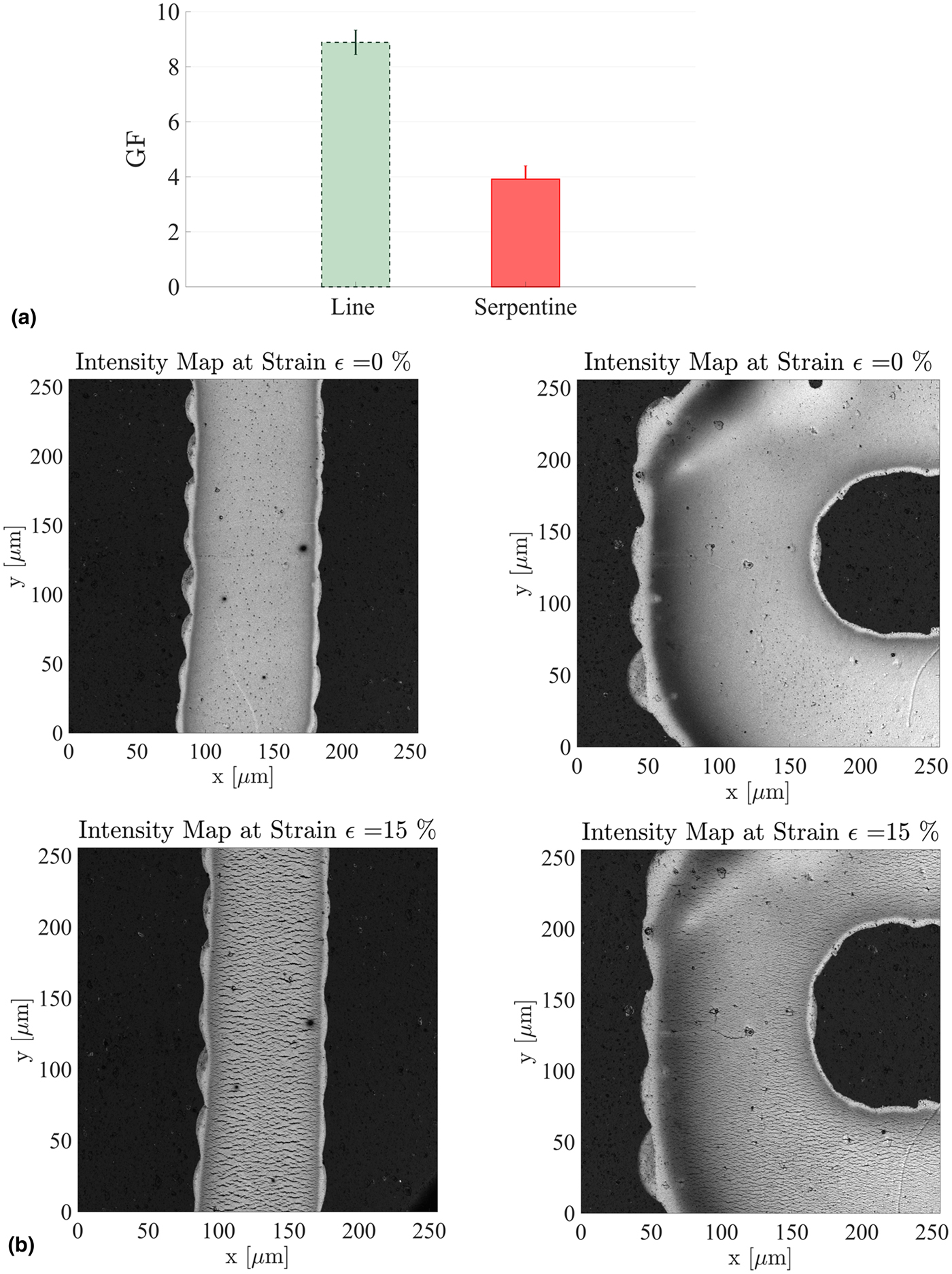
Electromechanical tests were performed on both the two geometries in order to understand the influence of the geometry on the reliability of the printed interconnects on PET substrate. As expected, serpentine exhibited higher deformability than the straight line. The gauge factor (GF), Fig. 3(a), calculated as the linear slope of the curve at 15% deformation, was used to compare the reliability of the two printed interconnects. The resistance variation of the serpentine shows a good linearity (R 2 = 0.995) with a GF of 3.9, which is lower than that of the line (GF 8.8). The resistance of the printed AgNPs tracks decreases under strain due to the formation of micro-cracks, as shown in Fig. 3(b). Increasing the tensile strain the cracks number increases and they become wider. A qualitative comparison between the two geometries shows that the serpentine, Fig. 3(b) right, presents lower density of cracks than the linear one, Fig. 3(b) left at the same deformation (15%).
(a) Gauge factor, calculated as the linear slope of the curve at 15% deformation, for line and serpentine interconnects. (b) CLM intensity maps of (left) line and (right) serpentine interconnect at 0% and 15% strain.

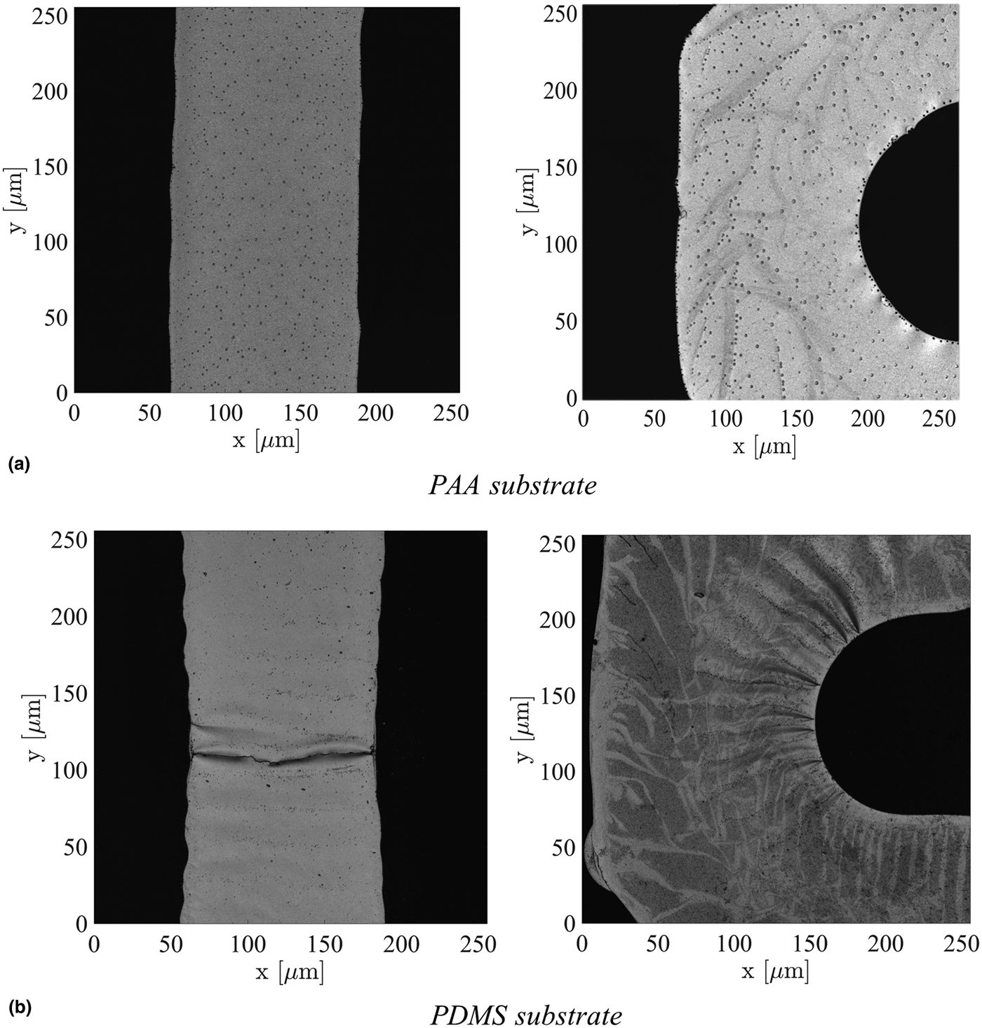
As concern the PDMS interconnects, Fig. 4(a) shows the printed patterns on the PAA substrate after the sintering process. Instead Fig. 4(b) shows the transferred printed interconnects on the PDMS substrate. Interconnects are characterized by fractures and wrinkles. These features occurred during the transfer process, as they were not present on the conductive tracks after the sintering of the AgNPs ink, Fig. 4(a), and also after the PDMS polymerization. The fractures and the wrinkles typology suggest that interconnects were subjected to an intrinsic compressive stress. When the strain of the substrate is released, due to the debonding of the PAA /PDMS interface, conductors are exposed to compressive strain, which causes conductors to buckle in an uncontrolled way. We assumed that these residual stresses were related to the PDMS shrinkage during polymerization. Since the shrinkage depends on the curing temperature,[Reference Madsen, Feidenhans, Hansen, Garnæs and Dirscherl19] PDMS polymerization was performed at room temperature and also a thinner layer of polymer was used. Despite these changes, we were not able to realize conductive interconnects with the proposed method.
CLM images of the inkjet printed interconnects, (left) line and (right) serpentine, on (a) PAA and on (b) PDMS substrate after the transfer process.

In order to overcome this problem, instead of PAA sacrificial layer, a commercial tattoo paper (Tattoo 2.1 The Magic Touch Ltd) was used, accordingly to the work of G. E. Bonacchini.[Reference Bonacchini, Bossio, Greco, Mattoli, Kim, Lanzani and Caironi20] The fabrication process is similar to the previous one, but at the end of the process a thin layer of ethyl cellulose (EC) remained on the top of the sample [Supplementary Information S.2]. This thin film protected the silver interconnects and guaranteed the integrity of the interconnects during the peeling process. However, the fabrication process is not reliable and few samples were successfully fabricated. One sample was characterized through an electromechanical test. The resistance reached an infinite value at low strain (around 4% of deformation), due to the break of interconnect [Supplementary Information S.3].
The optical analysis shows one wide fracture on the serpentine meander and on the EC film. Indeed, the fracture runs across the width of the interconnect and the EC layer, but not through the underneath PDMS which seems undamaged. No evidence of polymer/metal/polymer delamination were noticed, suggesting strong adhesion between AgNPs interconnect and both PDMS and EC layer. We can therefore assume that if PDMS can easily accommodate the applied deformation, the EC layer, which is the stiffest material, breaks at low strain dragging the interconnect and leading to fracture in the latter. These results show that the fabrication of stretchable PDMS interconnects through inkjet printing technique is still a challenge and further experiments and analysis should be performed in future.
Conclusion
Inkjet printing is a promising technique for the realization of cost-effective deformable electronics. However, different aspects should be considered because the reliability of the fabrication process and of the fabricated material systems are yet a goal to been reached. Therefore, an in-depth analysis of the manufacturing parameters was performed, and electromechanical characterization was achieved. The results showed the relevance of an accurate design of the geometrical layout that should be considered during the design phase. The electromechanical experiments confirmed that the geometrical layout strongly affects the electromechanical reliability of the printed interconnects: serpentine interconnections exhibited higher electromechanical reliability than the linear ones; although the directionality of the printing process should be considered when planning the geometrical features. Even if inkjet printing allows for printing versatile patterns directly from CAD drawings, the geometrical layout strongly affects the printing quality. This aspect particularly affects narrow and complex geometries, such as the serpentine interconnects. Therefore, the successfully reliable fabrication of serpentine interconnections is possible only after an accurate optimization of the printing parameters; in particular, drop spacing turned out to be one of the most important parameters to be tuned.
As for the samples on PDMS, the proposed transfer printing process was not a reliable fabrication method for the realization of the stretchable interconnects. The fabrication of interconnects on the elastomeric substrate is still a challenge. A further study on a suitable selection of the materials and the key factors for the fabrication of a flawless and electro-mechanically reliable stretchable silver interconnects should be performed.
Supplementary material
The supplementary material for this article can be found at https://doi.org/10.1557/mrc.2019.10.