I. INTRODUCTION
Recently, the application of radiofrequency identification (RFID) systems became more popular in different sectors such as industries, distribution logistics, libraries, and merchandise [Reference Dong, Ng, Yeung and Hai-Lan1, Reference Ajana, Harroud, Boulmalf and Hamam2]. The basic function of RFID systems is to retrieve automatically the information through a reader that has been previously inserted in a passive tag [Reference Lahiri3, Reference Lozani-Nieto4].
The whole communication between the reader and the tag involves two steps [Reference Chen, Chen and Li5]. In the first step, the reader radiates commands and the continuous wave (CW) to the tag. After receiving sufficient power from the radiated CW by the reader, tag wakes up and responds to the reader's communicated command. Secondly, in the process to send the signal to the reader, the tag antenna is alternatively connected to two different load impedances as per the data stored in the chip.
The CW is modulated by this process and is scattered back to the reader. When the difference between the lower and upper levels of the backscattered wave becomes sufficient, the reader would be able to demodulate the back scattered signal properly. Therefore, a proper tag design should be able to continuously provide sufficient power for tag chip while exhibiting the maximum level difference in the backscattered fields.
The communication distance between the reader and the tag is an important parameter in the RFID system to get wide area communication. This parameter is called read range. The Read range depends on various factors such as transmission power, frequency, gain of the reader and tag antennas, aperture of the antenna, the quality factor of the antenna, sensitivity of the reader, modulation type, radar cross-section (RCS), and the application environment [Reference Tang, He, Hou and Li6, Reference Mapa, Aryal and Chanda7]. Further, a successful antenna design must satisfy a conjugate impedance match condition [Reference Want8]. Along with these, for various application purposes, RFID tags need to be small. To meet these requirements, several RFID tag antennas have been proposed that operate in UHF band. Some compact antenna structures have been reported using inductively coupled structure [Reference Kim, Kim and Choj9–Reference Kim, Choi, Choi, Pyo and Chae14], inverted-F [Reference Soras, Karaboikis, Tsachtsiris and Makios15, Reference Hirvonenen, Pursula, Jaakkola and Laukkanen16], meandered antenna [Reference Chen, Chen and Li5, Reference Soliman, Sallam, Raedt and Vandenbosch17, Reference Bae, Lee, Chang, Kwon and Yoon18], and some other techniques [Reference Marrocco19–Reference Naji and Fyath21]. In [Reference Kim, Kim and Choj9–Reference Bae, Lee, Chang, Kwon and Yoon18] utilizes conventional single-antenna structure while some other utilizes dual-antenna structure [Reference Chen, Chen and Li5, Reference Chen, Chen and Li20–Reference Kamalvand, Pandey, Meshram and Mallahzadeh22]. Since the conventional single-antenna element RFID tag uses a single antenna for both the receiving and backscattering, it has some inherent limitations. The tag chip alternatively changes its impedances between highly complex values which are complex conjugate matched to antenna impedance and a short-circuit value. During the short circuit, the antenna will not receive any power (CW) from the reader; therefore, the efficiency of the energy absorption drops significantly in this phase. Further, the two impedance conditions, short circuit and conjugate matched, would not provide the maximum impedance difference in the backscattered signals, which results in shorter read range. To mitigate the limitations of the conventional single-antenna structure, RFID tags with dual-antenna structures have been reported. In [Reference Chen, Chen and Li5, Reference Chen, Chen and Li20], the dual-antenna structure is proposed with two meandered line antennas placed on the both sides of the substrate and operating in UHF bands. Whereas in [Reference Naji and Fyath21] dual-fractal antenna structure has been proposed which operates at 5.8 GHz and printed on both side of the substrate. Since both the antennas reported in [Reference Chen, Chen and Li5, Reference Naji and Fyath21] are placed on the either sides of the substrate, then it is very difficult to use these tags on the metallic surfaces and they do not have high differential RCS and gain. However, in [Reference Kamalvand, Pandey, Meshram and Mallahzadeh22] a single-sided platform-tolerant dual-antenna RFID tag is presented, but it has large size and to improve the read range complex technique of using mushroom-type electromagnetic (EM) band gap structure is utilized. Therefore, it is highly desirable to design an easy to fabricate RFID tag antenna that can mitigate these limitations.
In this paper, a single-sided novel dual-antenna structure for UHF RFID tag with significant enhancement in read range is proposed. The proposed tag consists of two independent antennas. One antenna is exclusively used for receiving and the other for backscattering. This technique provides the maximum and continuous power supply along with the maximum difference level of RCS in the backscattering mode, simultaneously. The performance of the proposed antenna is evaluated on the basis of differential RCS and read range. Table 1 summarizes the performance comparison such as size, operating frequency, increased read range, increased RCS, and type of antenna structure. It is observed that proposed easy to fabricate single-sided antenna structure has significant enhancement of read range and ΔRCS as compared with the other antenna structure at the cost of some increase in size. Further, the single-sided antenna structure helps to provide better performance when placed on different objects for operations. The concepts of dual-antenna structure along with antenna design are discussed in the following sections of the manuscript with the simulated and measured results.
Comparison of reported dual-antenna structure for RFID applications.

II. THEORICAL BACKGROUND OF DUAL-ANTENNA STRUCTURE
Figure 1(a) shows the configuration and equivalent circuit of a passive RFID tag. Figures 1(b)–1(c) show the schematic of both the conventional and the proposed dual-antenna along with tag ICs. The proposed dual-antenna structure works with a tag IC having three terminals instead of two terminals in conventional tag ICs for single-antenna structure, as shown in Figs 1(b)–1(c). The three terminals of tag IC for dual-antenna structure are denoted as RF1, RF2, and common ground. RF1 and RF2 are connected to the signal terminals of the receiving antenna and the backscattering antenna, respectively. The ground terminal is connected to the other terminals of both the antennas. In the proposed tag design, the backscattering antenna should be connected directly to the switching transistor, which is controlled by the backscatter modulator and provides either open- or short-circuited impedance loading for the antenna [Reference Chen, Chen and Li5, Reference Naji and Fyath21, Reference Balanis23, Reference Nikitin, Rao, Lam, Pillai, Martinez and Heinrich24].
(a) Configuration and equivalent circuit of a passive RFID tag, (b) schematic representation of conventional, and (c) schematic representation of dual-antenna tag IC.

For proper operation of RFID tag, receiving and backscattering antennas must satisfy the following conditions [Reference Chen, Chen and Li5, Reference Naji and Fyath21, Reference Green25]:
 $$Z_{reant} = Z_{chip}^* \quad {\rm and}\quad X_{bsant} = 0,$$
where Z reant , Z* chip , and X bsant are the impedance of receiving antenna, complex conjugate of chip impedance, and reactance of backscattering antenna, respectively.
In view of the two conditions given in equation (1), the maximum read range can be achieved. The maximum read range (d max ) of the tag antenna is given as [Reference Chen, Chen and Li5, Reference Aleksieieva and Vossiek26]:
 $$d_{max} = \left( {\displaystyle{{P_tG_t^2 \lambda ^2} \over {{(4\pi )}^3S_R}}\Delta \sigma} \right)^{1/4},$$
where λ, free space wavelength at operating frequency; P t , power radiated by reader; G t , gain of the reader antenna; S R , sensitivity of reader circuitry; and Δσ is the differential RCS between two loading states (open and short) of backscattering antenna.
Further, the RCS can be calculated as [Reference Nikitin and Rao27, Reference Harrington28],
 $$\sigma = \displaystyle{{\lambda ^2G_r^2 R_a^2} \over {\pi \vert Z_a + Z_L \vert ^2}},$$
where Z a (antenna impedance) = R a + j X a and Z L = impedance of chip.
The realized gain (G r ) of the receiving antenna can be defined as [Reference Virtanen, Bjorninen, Ukkonen and Sydanheimo29],
 $$G_r = \eta _r\eta _{cd}D = (1 - \vert {\rm \Gamma} \vert ^2)\eta _{cd}D,$$
where η r is the efficiency due to impedance mismatches, η cd is the efficiency due to conductor and dielectric losses (i.e., radiation efficiency), and D is the directivity of the antenna, and Γ is the power reflection coefficient.
III. ANTENNA STRUCTURE AND DESIGN
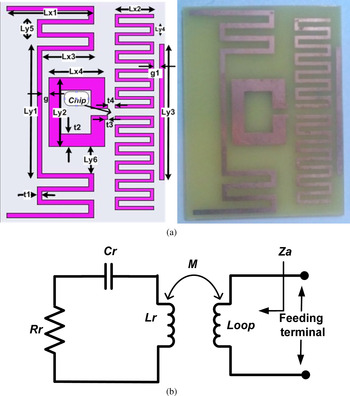
The configuration and fabricated prototype of the proposed antenna for RFID tag are shown in Fig. 2(a). It is fabricated on a low-cost FR4 substrate having dielectric constant (ε r ) 4.4, loss tangent of 0.018, thickness 1.6 mm, and overall size 50 × 67 mm2. The proposed dual-antenna consists of two independent antennas. One is made up of a meandered radiating element inductively coupled with a small rectangular loop as a feeding element, which acts as receiving antenna.
(a) Geometry and fabricated proposed dual tag antenna and (b) equivalent circuit of the inductively coupled feed structure.

Whereas the other one is meandered dipole antenna, along with a parasitic strip, which acts as backscattering antenna. The design concept of the proposed antenna in receiving mode is based on the paper reported in [Reference Chen, Chen and Li5].
The coupling strength of receiving antenna is controlled by the distance between the rectangular loop and the radiating element. Figure 2(b) shows the equivalent circuit of the inductively coupled feed structure. The inductive coupling is modeled by a transformer.
The input impedance of the receiving antenna (Z a ) is given by [Reference Son and Pyo10, Reference Sun, Xie and Cao11]
 $$Z_a = R_a + jX_a = Z_{loop} + \displaystyle{{{(2\pi fM)}^2} \over {Z_r}},$$
 $$R_a = \displaystyle{{{(2\pi f.M)}^2} \over {R_r}},$$
 $$X_a = 2\pi fL_{loop}.$$
From equations (5)–(7), it is observed that R a , M, and X a are functions of L loop , so they are separately controllable and could be adjusted for different RFID chips with different input impedances.
The proposed antenna is designed for Alien IC Higgs tag chip, which has an input impedance of 13.5-j110 Ω at 925 MHz [30]. The optimized values of shape parameters of the proposed antenna are shown in Table 2.
Dimension of proposed antenna structure.

IV. RESULT AND DISCUSSION
A) Parametric study
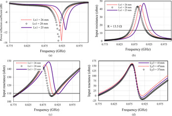
All simulations are performed using the Ansoft's high-frequency structure simulator (HFSS) [31] that uses finite-element method as the numerical technique to solve the EM problems. Variation of simulated power reflection coefficient, the real and imaginary parts of the input impedance of the receiving antenna and that of the chip by tuning the Lx1 with fixed Ly2 = 20 mm are shown in Figs 3(a)–3(c), respectively. It is observed that at the frequency of 925 MHz, the real part of the input impedance of the receiving antenna is tuneable between 24.4 and 8.4 ohm, while the imaginary part is almost same and varies a little from 109 to 113 Ω.
Simulated (a) power reflection coefficient, (b) real part of input impedance, (c) imaginary part of input impedance of receiving antenna by tuning the Lx1 when Ly2 = 20 mm, and (d) imaginary part of input impedance of backscattering antenna by tuning Ly3 when receiving antenna is matched.

Figure 3(d) shows the variations of the imaginary part of the input impedance with the frequency under the matched receiving antenna condition, for the backscatter antenna by tuning the vertical length of backscatter antenna (Ly3) with fixed Lx1 = 26 and Ly2 = 20 mm. It can be clearly seen that to satisfy equation (1), the imaginary part of backscattering antenna should be close to zero for achieving maximum differential RCS and for Ly3 = 41 mm the value of reactance close to zero is obtained.
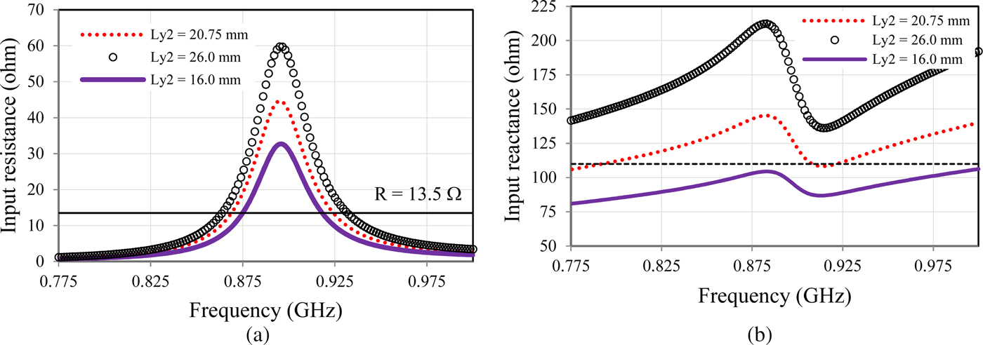
Further, Figs 4(a) and 4(b) show the real and imaginary part of the input impedance of the receiving antenna by tuning the Ly2. It is observed that, at a frequency of 925 MHz, the imaginary part of the input impedance of receiving antenna is tuneable from 88 to 141 Ω, whereas little variations of 8–18 ohm are there in the real part for Lx1 = 26 mm.
Simulated (a) real part and (b) imaginary part of input impedance of receiving antenna by tuning Ly2 when Lx1 = 26 mm.

Rigorous analysis is carried out on the other shape parameters (presented in Table 2) of the receiving antenna to achieve the complex conjugate value of the chip. The input impedance of the receiving antenna is obtained 13 + j111 ohm at 925 MHz frequency, which is close to the complex conjugate of the chip (13.5-j110 Ω) by choosing the optimized values of the various shape parameters of the antenna. The proper impedance value of the antenna is required to minimize the reflection losses between the antenna and chip, and hence, improve the transmitted power and maximize the read range.
B) Simulation and measurement results
There are several RFID Tag antenna characteristics measurement techniques in the literature [Reference Camp, Herschmann, Zelder and Eul32–Reference Frickey39]. In [Reference Qing, Goh and Chen36–Reference Palmer and van Rooyen38], very feasible, inexpensive technique for the measurement of the balance RFID tag antenna was proposed which is known as differential probe method. The concept of this method involves the measurement of the S-parameters to calculate the differential input impedance between ports of the antenna with the help of differential probe. The differential input impedance is the actual complex input impedance of the antenna.
The differential input impedance can be expressed by using S-parameters as follows [Reference Frickey39]:
 $$Z_d = \displaystyle{{2Z_0(1 - S_{11}S_{22} + S_{12}S_{21} - S_{12} - S_{21})} \over {(1 - S_{11})(1 - S_{22}) - (S_{21}S_{12})}}.$$
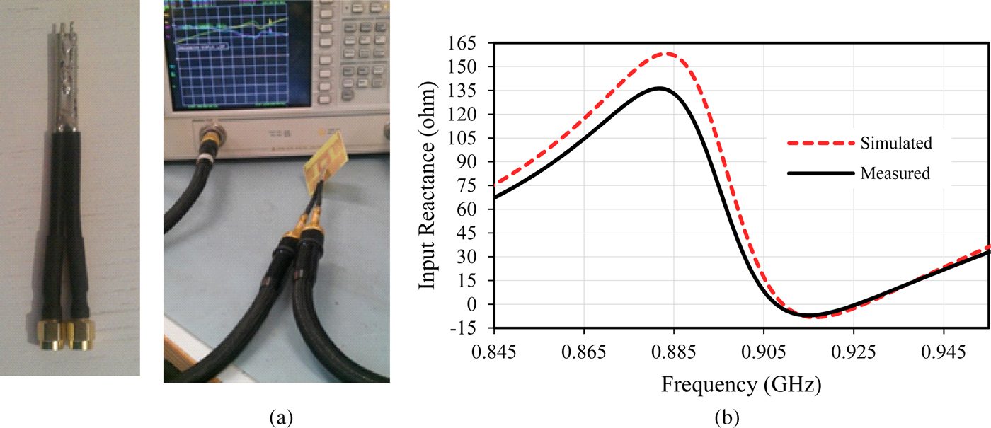
To measure the characteristics of the proposed RFID tag antennas, we have fabricated the differential probe as mentioned in [Reference Qing, Goh and Chen36–Reference Palmer and van Rooyen38]. Figure 5(a) shows the differential probe with measurement setup. With the help of differential probe connected to the terminals of antenna, S-parameters for two ports of differential probe are measured. Using the values of the S-parameters, differential input impedance is calculated. Further, with the help of differential input impedance, power reflection coefficient is calculated [Reference Nikitin, Rao, Lam, Pillai, Martinez and Heinrich24].
(a) Differential probe with measurement setup and (b) simulated and measured input reactance of backscattered antenna with optimum values.

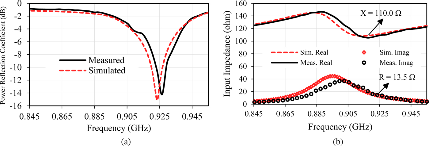
The simulated and measured input reactance of backscatter of antenna is shown in Fig. 5(b). The measured reactance values of the backscattering antenna are observed as −2.4 ohm which is close to zero. The simulated and measured results are in good agreement as seen from the plots. Figure 6 shows the simulated and measured results of reflection coefficient and input impedance of receiving antenna. The measured complex input impedances for the receiving antennas is obtained as 13 + j109 Ω, which is close to the complex conjugate of the chip impedance, i.e. (13.5 + j110 Ω). Due to the good impedance matching, low value of the reflection coefficient is observed about 0.925 GHz and shows antenna work properly.
Simulated and measured (a) reflection coefficient and (b) input impedance of the proposed antenna with optimum values.

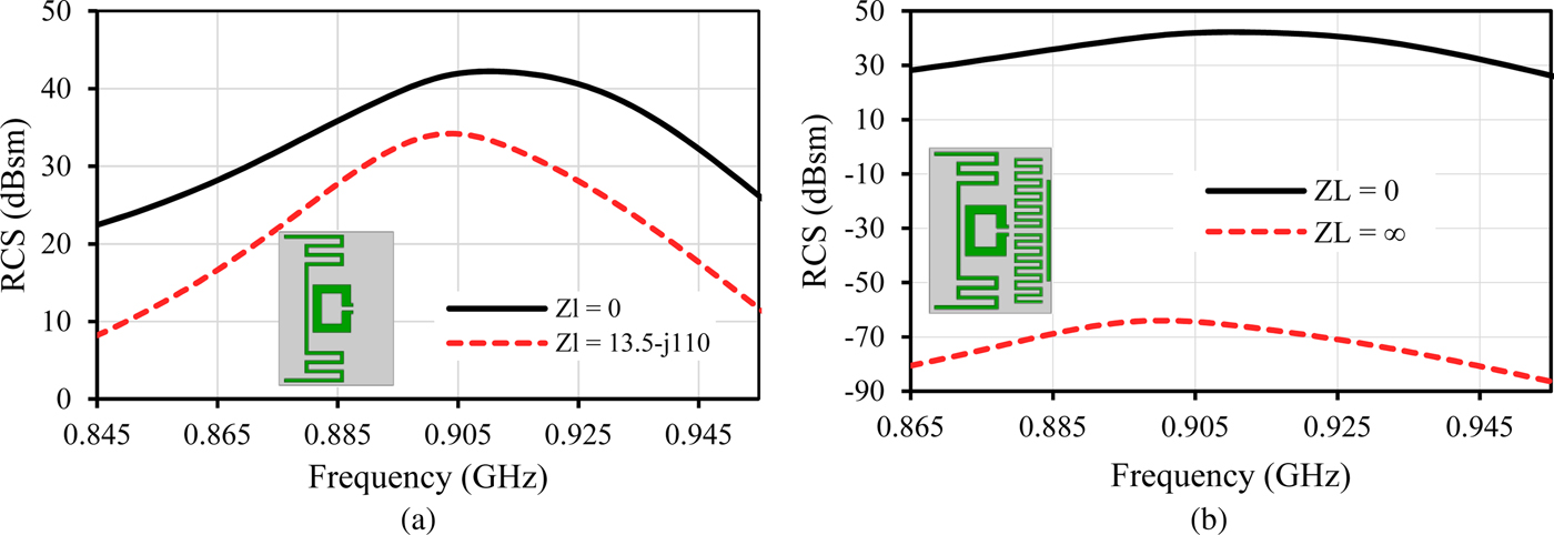
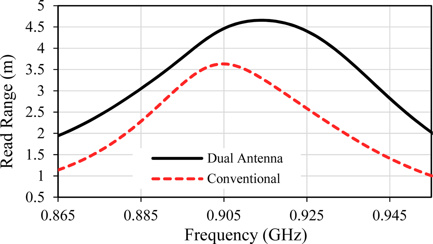
RCS of the proposed dual antenna is compared with conventional single-antenna structure in Figs 7(a) and 7(b). It is observed that the differential RCS (Δσ) in open and short-circuit states of the proposed dual-antenna structure is increased. Since the read range is directly proportional to the differential RCS under the two loading impedance, it results in the enhancement of read range, as shown in Fig. 8. With the help of the dual structure, we have managed to maximize the quantity of Δσ from 12 to 110 dBsm. It increases the read range from 2.4 to 4.4 m. It is noted that the receiving antenna of proposed dual-antenna structure is conjugate match; whereas the backscattered antenna alternatively switches between open and short-circuit states.
RCS of (a) conventional antenna in two states (matched and short circuit) and (b) proposed antenna in two states (open and short circuit).

Read range comparison of the conventional and proposed antenna.

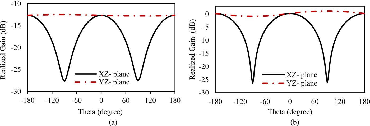
The simulated radiation pattern in terms of realized gain for the receiving and backscattering antenna in the xz- and yz-planes at 915 MHz is presented in Fig. 9. Both the antennas of the RFID tag show the omnidirectional pattern as required by the short-range communication devices, with dumbbell shape variation in the xz-plane and nearly non-directional variation in the yz-plane. The back scattering antenna has deep null in the xz-plane and more variation in the yz-plane than the receiving antenna.
Radiation pattern of (a) receiving antenna and (b) backscattering antenna at 925 MHz.

V. CONCLUSION
In this paper, a novel meandered dual-antenna structure for UHF RFID tag is presented. Both the antennas are printed on one side of the substrate. One of the antennas is exclusively used for receiving in order to provide the maximum power transfer to the tag chip. Other one is used for backscattering and designed to provide the maximum differential RCS. The design of the dual structure is discussed and the input impedance of both antennas with aid of differential technique is measured. By using the dual-antenna structure, the read range of UHF RFID system increased significantly.
ACKNOWLEDGEMENT
G. K. Pandey is grateful to the University Grant Commission (UGC) New Delhi, India for providing financial support in terms of senior research fellowship (SRF).
 Pouria Kamalvand was born in Shiraz, (Fars), Iran, in 1982. He received his B.Tech. degree in Electronics Engineering from the Islamic Azad University, Arak branch, Iran in 2005 and the M.Sc. degree in Electronics Engineering from Islamic Azad University, Bushehr branch, Iran in 2009. Currently, he is working toward his Ph.D. degree in the Department of Electronics Engineering, Indian Institute of Technology (Banaras Hindu University), India. His research interests include Microstrip antenna, RFID tag antenna, Dual structure, Dual band antenna, Wide Band antennas, and Electromagnetic Bandgap structures (EBG).
 Gaurav Kumar Pandey received the B.Sc. degree from St. Andrew's College, Gorakhpur and the M.Sc. degree in Electronics from Deen Dayal Upadhyay Gorakhpur University, Gorakhpur, Uttar Pradesh, India, in 2007 and 2009, respectively. Currently, he is working toward his Ph.D. degree. His research interests include Microstrip antenna, UWB antennas, Metamaterials, Electromagnetic Bandgap structures (EBG), MIMO antennas for handheld devices, Tapered slot antenna, RFID tag antenna, and microwave imaging. He has published more than 40 papers in national and international journals and conferences. He is also working on a project funded by Defence Avionics Research Establishment (DARE), Defence Research and Development Organization (DRDO), India.
 Manoj Kumar Meshram received Ph.D. degree from the Department of Electronics Engineering, Institute of Technology, Banaras Hindu University, Varanasi, India, in 2001. In 2002, he joined as a Lecturer in the Department of Electronics Engineering, Indian Institute of Technology (Banaras Hindu University), Varanasi, India, where presently he is working as Assistant Professor. He received INSA (Indian National Science Academy) Fellowship 2008–2009 from Govt. of India to visit South Korea under bilateral exchange program. In the year 2010, he has been awarded with the BOYSCAST fellowship for 1 year for conducting advance research at McMaster University (Electrical and Computer Engineering), Hamilton, Ontario, Canada, with Professor Natalia K. Nikolova. He has published more than 75 research papers in referred international journals and conferences. His research interests include frequency scanning antenna, microstrip antenna, UWB antennas, MIMO antennas, tapered slot antenna, ferrites, MMIC, and microwave imaging. Dr. Meshram is a Senior Member of IEEE and a Life Member of the Institution of Electronics and Telecommunication Engineers (IETE), India.