I. INTRODUCTION
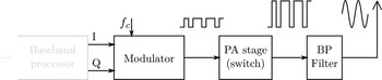
The growing demands toward a highly efficient, flexible, and low-cost wireless infrastructure have been fueling the research on microwave power amplifier (PA) concepts within the last years. As the RF PA is the last analog part in the transmitter chain of today's base stations, increasing attention is paid to digital amplifier solutions, partly referenced to as class S [Reference Hung, Rode, Larson and Asbeck1, Reference Wentzel, Chevtchenko, Kurpas and Heinrich2]. Figure 1 illustrates the principle of such a digital microwave PA: the incoming digital IQ baseband signal is encoded into a binary pulse sequence containing the wanted signal at carrier frequency f c . This pulse sequence is amplified by a binary PA, i.e. a switch. A band-pass filter between PA output and antenna then restores the wanted analog microwave signal. A key component in this architecture is the modulator, which translates the input signal into a stream of binary pulses that is adapted to the digital PA characteristics. The choice of modulation scheme is dictated by the requirements to meet the ACLR and EVM specifications as well as to offer high coding efficiency, so that the PA can be operated as efficiently as possible.
Concept of a digital microwave PA.

Please note, despite the similar name of the digital PA modulator block and the baseband modulator that is used to create the IQ baseband signal in the first place, there is no further connection between these two blocks. The modulator concept for digital PAs presented in this paper does not include any baseband processor and does not impose any restrictions on the baseband modulation. Instead, the combination of (digital PA) modulator, digital PA, and band-pass filter is a fully transparent replacement for an analog upconverter and amplifier. It can work on any baseband signal with finite bandwidth.
So far, mainly pulse-width (PWM) and delta-sigma modulation (DSM) have been used as coding schemes for digital microwave PAs. The time-continuous and analog nature of a PWM implementation not only requires a fast and precise digital-to-analog converter (DAC) with tightly tolerated components but furthermore excludes it from the benefits, which technology downscaling offers for digital circuits. In contrast, band-pass DSM (BPDSM) is an all-digital implementation, but has a very low coding efficiency which, in turn, lowers the overall efficiency of any real, and thus non-ideal digital PA. (Coding efficiency is defined as the in-band signal power divided by the total power of the signal, including DC.) There have been first efforts to combine (quantized) PWM with DSM in [Reference Markert, Haslach, Heimpel, Pascht and Fischer3]. But while simulation results look promising, actual measurements suffer from low ACLR values. However, all these modulators share the inability to compensate for distortions created by the amplifier on their own. Instead they require a computationally intensive digital predistortion (DPD), thus reducing the overall efficiency.
In this work, we propose a new modulator concept based on a wavetable, which respects the limitations a digital implementation imposes, e.g. finite-time resolution and limited clocking rate. Moreover, it is adjustable to special amplifier needs like dynamic dead times between PA inputs, minimum pulse length limit, or even multiple amplifier inputs. Furthermore, it features a very high coding efficiency and can correct for amplifier non-linearities with very small or even no additional computational resources.
The paper is organized as follows: Section II describes the coding scheme, Section III evaluates the modulator performance using simulations, while Section IV presents actual measured results. Section V concludes the paper.
II. CODING SCHEME
The input signal of a simple amplifier with one input and one output can be seen as having two degrees of freedom: its voltage level (amplitude) and timing information (phase). A digital PA reduces the amplitude to a discrete set of values. In its most basic form, the binary case, it is only capable of switching between two distinct output potentials. Therefore, all other signal information has to be encoded in the timing of the signal, which still can apply very high resolution as the amplifier is a time-continuous system. Many time-continuous modulators such as PWM [Reference Maier4], Click [Reference Wagh, Midya and Rakers5], or Neoteric [Reference Schemel6] exploit the accuracy that can be accomplished by fully utilizing the non-discrete nature of the timing information; but they suffer from implementational problems related to their analog nature, like the need for tightly tolerated components, high-power consumption, and considerable chip size requirements. On the digital side, the two common implementations are envelope DSM (EDSM [Reference Hori, Kunihiro, Takahashi and Fukaishi7, Reference Tanio, Hori, Hayakawa, Tawa, Motoi and Kunihiro8]) and BPDSM. While EDSM suffers from poor ACLR values [Reference Tanio, Hori, Hayakawa, Tawa, Motoi and Kunihiro8], BPDSM has a very low coding efficiency [Reference Johnson, Shawn and Stapleton9]. Therefore, to increase overall performance and signal accuracy, it is desirable to utilize more different pulse lengths, taking advantage of the non-discretized nature of the signal timing.
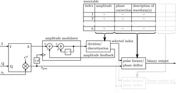
The new approach presented in this paper features a digital modulator that runs on an average clock rate of f c (carrier frequency) or even on integer divisions of that if further restrictions on the output filter can be accepted. Only a final pulse-forming circuit needs oversampling techniques and (digital) delay lines to shift pulse edges. The proposed modulator concept is designed to be adapted to many different hardware configurations. Its aim is to maximize the utilization of any given pulse-forming circuit regarding its timing and pulse-shaping capabilities. Figure 2 illustrates the new concept. It consists of a first block that processes the baseband IQ samples into an amplitude value and a constant amplitude but phase-modulated version s pm of the carrier signal s c . These signals are then further processed by an amplitude modulator with a decision and discretization unit and a pulse-forming waveform generator.
Block diagram of proposed wavetable modulator concept.

The decision and discretization unit selects one line of the wavetable based on the available amplitude values and its internal selection algorithm. The index of the selected wavetable entry is then sent over to the pulse former, which uses the phase correction value and the waveform description of the corresponding wavetable entry to create the output signal. For amplifiers that need more than one input signal, there might be several pulse former circuits running in parallel. Each of those is driven by the same clock and index value signals, but feature their own phase and waveform description columns in the accordingly extended wavetable.
A) Waveform generator
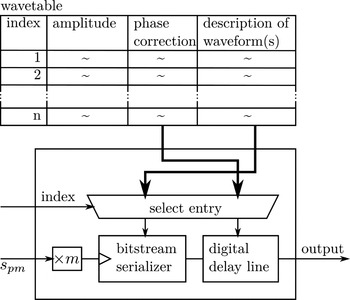
For this paper, a pulse-forming hardware as depicted in Fig. 3 is assumed. It consists of a bitstream generator with an oversampling factor of m combined with a digital delay line. This kind of hardware is already available in many field-programmable gate arrays (FPGAs) and other complementary metal-oxide-semiconductor (CMOS) processes as a SerDes device. With the index value from the decision/discretization unit, one row of the wavetable is selected. The bitstream serializer generates the desired pulse form, while the phase correction value is handled by the delay line. For d = 1, this results in one waveform description from the wavetable being placed over the time span of exactly one period of s pm .
Pulse forming circuit of Fig. 2 in detail.

The actual waveform descriptions stored in the wavetable are specially designed based on the capabilities of the pulse former. If the serializer expects a vector of m bits to shift out in sequence, it would probably be most suitable to store this vector as-is in the wavetable. Designing an optimal set of waveforms can become a very difficult process, since usually there are several different waveforms that result in the same amplitude once they passed the amplifier and band-pass filter. This especially holds true, when amplifiers with more than one input are considered (outphasing, multi-level, etc.); but this complexity in the design phase also gives the designer the opportunity to select an optimal balance between design goals of the overall system (e.g. best ACLR versus best efficiency). Moreover, since the wavetable is stored in memory, it can easily be exchanged by another one as needed. For example, if the baseband back-end switches to another communication standard that allows for lower ACLR, an updated wavetable can be used that treats in ACLR for amplifier efficiency without any changes to the hardware. The influence of the number of available amplitudes in the wavetable can be seen in the first part of Section III where a variation of m directly corresponds an accordingly adapted number of rows in the wavetable.
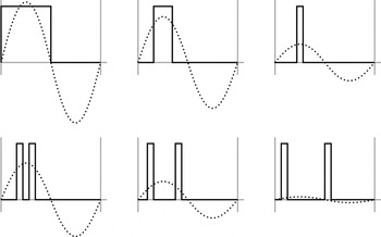
In general, for a higher oversampling ratio m, there will be more different waveforms, i.e. more rows in the wavetable, than for lower oversampling ratios. The waveform is also not necessarily limited to a single pulse with a varying duty cycle. Instead, e.g. it could consist of two pulses that are not only varied in their width, but also in their distance, partially canceling out each others contribution to the resulting output signal after the band-pass filter (see Fig. 4). This would lead to a higher resolution of amplitude values (more increments) after the final output filter than by only varying the pulse width. A combination of both approaches is possible as well in various forms.
Examples for varying the resulting amplitude by adjusting either the width of one pulse or the distance between two pulses. Solid: designed pulse form; dashed: signal after BP filter.

While using three or even more pulses per waveform is possible, it is typically not advisable, because the efficiency of any real amplifier will decrease. In this step of designing suitable waveforms special requirements of the amplifier like, e.g. maintaining a certain minimum pulse length can be considered by removing not suitable waveform entries. In general, more entries in the wavetable lead to better signal accuracy because more amplitude values can be encoded in the pulse form itself, i.e. as time information. Thus, the amplitude modulator has more values to choose from, resulting in accordingly reduced quantization noise. This again lowers the filter requirements. For each entry in the wavetable, the resulting amplitude and phase values are stored along with each waveform for later use. These values are either precalculated or the result of a distortion correction pass as described in Section II.C.
B) Amplitude modulator and discretization
The amplitude modulator as shown in Fig. 2 is similar to a DSM, but instead of using the common binary or multibit discretizer with equally spaced increments, a specific discretization unit is used. The amplitude modulator does not have to be of DSM type, but can be any form of modulator that can be clocked at an appropriate rate or even no modulator at all using only the discretization unit; but due to its noise-shaping properties and the simple implementation, a DSM-type modulator is a promising candidate. For all results presented in this work, a second order DSM was used.
In its simplest form, the discretization unit reads in all amplitude values from the wavetable and does a nearest neighbor decision with respect to the input signal. The chosen amplitude value is sent into the feedback loop of the modulator, while the index number of the chosen wavetable entry is relayed to the pulse generator. In this way, the actual capabilities of the pulse generator are already considered inside the amplitude modulator.
For future work, it would be possible to include a more sophisticated decision approach in the discretization unit. For example, instead of using a nearest neighbor decision for all samples, some of them could be forced to a zero waveform (i.e. no pulses) to reduce switching losses in the amplifier. Since this will happen inside the feedback loop of the modulator, it will inherently compensate for the skipped pulses in the following samples.
Another interesting approach would use two wavetables with different sets of waveforms, where one table is optimized for high signal amplitudes and the other one for low amplitudes. The decision unit would then switch between the two tables based on the input signal amplitude with a well-chosen hysteresis or even using a fetch-ahead path of the amplitude for the decision, if a small amount of latency is acceptable. However, having to many switchovers between (radically) different wavetables would lead to an increased amount of unwanted spectral components; but if carefully designed, any complex decision scheme can be realized inside the decision unit.
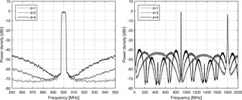
The clock divider d also can be varied, if required. This might be necessary in an actual application-specific integrated circuit (ASIC) implementation when the achievable clocking rate is lower than the carrier frequency. With d = 1, the amplitude modulator and discretization unit are clocked by s pm , providing exactly one index value to the pulse generator for every period of s pm , i.e. every period of the desired RF signal. For d > 1, each output sample of the amplitude modulator covers d periods of s pm . Then, the waveform description in the wavetable will cover d consecutive periods of s pm . This not only lowers the speed at which the amplitude modulator has to operate, but also enables more sophisticated pulse form variations, which again can be used to further reduce switching losses in the amplifier or to account for other properties of the amplifier. The disadvantage of using d ≥ 2 is the steeper raise of out-of-band noise, thus increasing the constraints on the output filter. Figure 5 shows how the spectral composition changes for different values of d. Table 1 reports on the key figures of the resulting signal. For the sake of simplicity, in this experiment, the waveforms in the wavetable were only expanded by concatenating them d times to theirselves. No additional entries were added nor were different waveform entries concatenated into a new one.
Frequency spectrum for different amplitude modulator clock division settings d.

ACLR and EVM values for different settings of d.

If different waveforms from the wavetable of d = 1 were combined to form new, additional entries for a wavetable for d ≥ 2, this on its own could improve the signal quality over the one shown in Fig. 5 since there are more different amplitude values to choose from. More rows (i.e. amplitude values) generally lead to reduced noise in the space between multiples of the carrier frequency. This idea could be even further extended if multiple sampling points of the amplitude signal were considered in each clock cycle of the DSM inside the amplitude modulator block. For example, if designing a system for d = 3 based on an existing system with d = 1 each waveform inside the wavetable now has enough space to accommodate the concatenation of three waveforms of the d = 1 case. Every possible combination of waveforms from the d = 1 table could be added as extra rows to the d = 3 table. Based on the absolute level and the differences of three sampling points of the amplitude signal taken at each clock cycle, a suitable row (i.e. combination of waveforms from the former d = 1 case) would be selected. In effect, this method would gradually lead closer toward a system that behaves like a paralleled DSM. Although possible, the method as described adds a lot of complexity to the DSM and the decision unit of the amplitude modulator. A complete weighing up of lowered clock rate versus added complexity and regained signal quality will greatly depend on the exact properties and constrains of any given ASIC technology.
C) Correction of amplifier distortions
As each RF PA as well as pulse generators are non-ideal, there will be signal distortions. The elongation or shortening of the pulses will result in amplitude errors and varying time delays over different waveforms will result in phase errors. Thus, a correction is needed to compensate for these effects, helping to fulfill the given linearity requirements (ACLR and EVM) of the amplifier system. In a static correction approach, actual amplitude and phase values for each entry of the wavetable will be recorded at the load output after the band-pass filter. This is done either by simulation or an actual measurement. These values are then written back into the corresponding column of the wavetable. Since the amplitude modulator now has more accurate amplitude values for each waveform, the resulting amplitude error will be greatly reduced, and the AM/AM intermodulation will be linearized. The phase error is corrected by the phase shifter inside the pulse generator. This static correction approach does not require any additional resources since it only adjusts already existing parameters to match the existing hardware more precisely. In laboratory experiments with digital PA prototypes, it was found that correction values, once determined, remained valid when they were loaded 4 weeks later. Of course, this only holds true as long as outer parameters (supply voltages, temperature) are not changed.
However, an adaptive correction approach can be used to additionally correct for effects that change over time (e.g. thermal effects, aging). For this method, a small segment of the output waveform is captured, downconverted, and compared with the baseband signal. Again, differences in amplitude and phase are calculated and the values of the wavetable are adjusted accordingly. The sampled segment can be from any signal, as long as it covers the full dynamic range. No special training sequence is required for this purpose. Furthermore, applying the newly calculated values to the wavetable is instantaneous, so that there is no down time of the amplifier and the signal is not interrupted.
The most outstanding feature of this approach over the traditional DPD is the fact that the traditional DPD, when applied to a digital PA system, would need to have a processing module in the signal path in front of the digital PA modulator in order to apply the inverse amplifier model to the incoming signal. Since this module has to process every sample of the incoming signal in real time, it would substantially add to the overall power consumption of the system, reducing the overall efficiency. This is even more true in systems with only a few Watts of RF output power per amplifier (massive MIMO, MicroCells, etc.). The method presented here, in contrast, only refines internal values of the digital PA modulator (i.e. the wavetable). By that it is a one-time operation with no need to process the whole signal. All signal processing is handled by the already existing digital PA modulator as it would without any applied correction, thus consuming no additional power for applying the predistortion to the signal.
III. SIMULATION RESULTS
In order to demonstrate the performance of the proposed modulator, a Matlab model was implemented. This section covers some parameter variations and studies their influence on the resulting output signal characteristics. Unless stated otherwise, parameters are chosen to be f c = 900 MHz, d = 1, m = 64 with a second-order DSM as amplitude modulator and a time resolution of 1 ps for the delay line. A WCDMA-like signal with 6.5 dB peak-to-average power ratio (PAPR) and a nominal bandwidth of 5 MHz is used as input. The wavetable is generated to contain waveforms with a single pulse per period, only varying the width of this pulse in discrete time steps, in accordance with the serializer clock frequency. A one-bit output is assumed (binary signal, i.e. a pure binary amplifier is used).
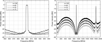
In a practical implementation, the maximum clocking rate of the serializer will be limited by technology available. Since the average clocking rate is determined by the carrier frequency times m, for a given carrier frequency, maximum m will be linked to the technology used. A reduced value of m will result in fewer possible waveforms and by thus reduces the number of rows (i.e. different amplitude values) in the wavetable. Figure 6 shows how different values for m affect the spectrum of the output signal. While the influence on the noise level directly adjacent to the wanted signal is very weak, noise at 450 MHz rises by about 6 dB when m is halved. Accordingly, this directly influences the output filter demands as it needs to provide a higher suppression. The influence on the noise directly adjacent to the wanted channel is given as ACLR measurement data in Table 2. The coding efficiency, however, is not affected by the oversampling ratio m. The amplitude of the in-band portion stays the same (see Fig. 6) for all values of m. The energy content in between multiples of the carrier is slightly higher for lower values of m, but this gets compensated by reduced amplitudes at multiples of the carrier frequency. Spectral peaks at
 $f_c \cdot m \cdot N,N \in {\open{\rm Z}}_{ \ne 0}$
also cancel out.
Frequency spectrum for different oversampling factors m.

Corresponding ACLR and EVM for Fig. 6, measured over 5 MHz wide channels.

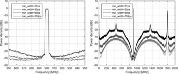
By removing entries with very short pulses from the wavetable, it is possible to accommodate for an amplifier that is either very inefficient when operating with such short pulses or cannot generate them at all. As can be seen in Fig. 7, elongating the minimum pulse length produced by the modulator has a strong and non-linear impact on the unwanted spectral components. Especially for a minimum pulse length of 139 ps noise increases significantly. Only the noise level directly adjacent to the wanted channel is not increased by a great amount (see Table 3). This behavior can be understood by realizing that the minimum amplitude that can be encoded with a single pulse per period when setting a limit of 139 ps at 900 MHz carrier frequency is −8.34 dBFS. The given input signal for this simulation is lower than this value for 85% of the time. Since lower amplitudes than this threshold will be encoded by skipping pulses, the modulator essentially is turned into a pulse-skip-modulator (PSM) for this duration, inheriting some of the unfavorable spectral properties of the PSM. In case this effects becomes the limiting factor in a design, it might be reasonable to evaluate waveforms with two partially canceling pulses per period to realize low-amplitude values while still meeting the minimum pulse width requirement (refer to Fig. 4).
Frequency spectrum for different minimum pulse widths.

Corresponding ACLR and EVM for Fig. 7, measured over 5 MHz wide channels.

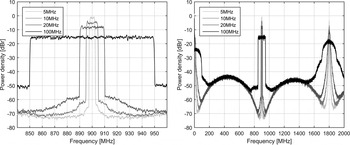
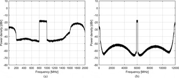
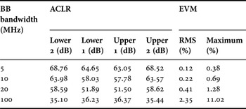
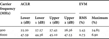
Another important factor for the resulting signal quality of the modulator is the bandwidth of the incoming baseband signal. Wider bandwidths increase the amount of signal content directly adjacent to the channel (see Fig. 8 and Table 4), consequently worsening ACLR. This effect, however, is coupled to the carrier frequency, enabling wider bandwidths at higher carrier frequencies. Figure 9(a) depicts a 200 MHz wide signal at a carrier frequency of only 900 MHz. Clearly, the performance of this setup in terms of ACLR is insufficient for most use cases. In contrast, the same baseband signal on a 6000 MHz carrier, as depicted in Fig. 9(b), is much more usable. Table 5 lists actual ACLR values as measured in the simulation. Note that for Fig. 9(b) not only the carrier frequency has been increased to 6 GHz, but also the value of m has been reduced to m = 16 (m = 64 was used for Fig. 9(a)). This was done to limit the serializer clock to a more feasible rate of 96 GHz. One should note, however, that 200 MHz bandwidth at 900 MHz carrier frequency correspond to about 22% relative bandwidth, which is higher than required for typical applications. Since future trends go toward higher carrier frequencies at 6 GHz and above, this problem becomes less important.
Frequency spectrum for different bandwidths of the baseband signal.

Frequency spectrum for a 200 MHz wide signal at 900 MHz with m = 64 and for the same signal at 6 GHz with m = 16.

Corresponding ACLR and EVM for Fig. 8; bandwidth and center frequency offset for measurement channel equals respective baseband bandwidths.

Corresponding ACLR and EVM for Fig. 9, measured over 200 MHz wide channels.

The coding efficiency for every signal shown in this section always remains at its theoretical maximum. The coding efficiency η
c
is defined as the in-band signal power of the digital bitstream divided by the total power of the bitstream [Reference Johnson, Shawn and Stapleton9]. As is shown in [Reference Johnson, Shawn and Stapleton9], the maximum coding efficiency for a full-scale sinusoidal tone is 81% and the total power of the bitstream is independent of its contents (since it always applies a voltage of either + Δ
a
or − Δ
a
to the load). For a WCDMA signal with 6.5 dB PAPR, the average in-channel power is 6.5 dB lower than the one of the full-scale tone. Therefore, the maximum achievable coding efficiency is
 $\eta _{c, - 6.5\;{\rm dB},\max} = 81\% \cdot 10^{( - 6.5/10)} = 18.1{\kern 1pt} \% $
. All signals discussed in this section reached this value. Between different settings, only the unwanted signal parts are distributed differently. For comparison, the BPDSM used in [Reference Johnson, Shawn and Stapleton9] reached only 7.1% coding efficiency for a 7.1 dB PAPR WCDMA signal.
IV. EXPERIMENTAL RESULTS
In order to also verify the performance of the proposed modulator in a real-world setup, the binary output sequence of the simulation was sent to a Keysight M8195A AWG and subsequently measured by a spectrum analyzer in frequency domain and a real-time oscilloscope for time domain characterization. The parameters for the modulator were chosen to be the same as in Section III.
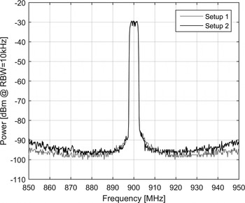
Figure 10 presents the measured frequency spectrum for two different setups. Setup 1 uses m = 32 and a minimum pulse length of one bit time, i.e. ≈34 ps. For setup 2 the bitstream serializer speed was increased to m = 64, but at the same time, a limit of six bit times, i.e. ≈104 ps, for the duration of the shortest pulse was introduced. The need to limit the minimum pulse length may arise if an amplifier shows strongly degraded performance for such short pulses. Due to the increased value of m the overall noise floor is lowered, while the increased minimum pulse length adds noise. Both effects cancel so that a comparable ACLR performance of over 57 dB is reached for both variants. Table 6 lists the measured data.
Measured frequency spectrum for two different modulator setups.

Measured ACLR and EVM values for two different setups over 5 MHz wide channels.

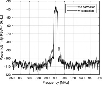
To examine the feasibility of the correction approach, the signal generator is connected to an analog broadband amplifier (SHF824) in order to add non-linearities on the digital pulse train. After attenuation, the signal is captured by the oscilloscope and correction values are calculated. For this setup, the following parameters were chosen: m = 32 with a minimum pulse length of one bit time (≈34 ps). f c and d remain at f c = 900 MHz, d = 1. To keep measurement times low, the signal length is reduced from 100 to 10 µs, which explains the noisier appearance of the frequency plots in comparison to the ones shown before.
Figure 11 shows the resulting spectrum after the amplifier before and after applying the estimated correction values to the wavetable. Table 7 collects the measured data. An improvement of over 10 dB in the ACLR performance in the adjacent channel was observed. With an ACLR of more than 58 dB, this system could easily meet the 3rd Generation Partnership Project (3GPP) criteria for cellular base stations (45 dB ACLR).
Frequency spectrum after the amplifier without and with correction.

Measured ACLR and EVM values over 5 MHz wide channels.

While this measurement used an analog broadband amplifier to prove the concept, the correction approach is tailored to suit digital microwave PAs, which do not provide a linear amplification but just switch between two states. Measurements on a prototype of such a digital amplifier have been conducted and will be published in [Reference Hühn, Wentzel and Heinrich10].
V. CONCLUSION
A new digital modulator concept using a wavetable approach has been developed and proven for the first time. Characteristic features of the modulator are that it accommodates flexibility of modulation types and its architecture is adapted to digital hardware building blocks. Simulations as well as measurements show excellent results in terms of signal quality. ACLR values of ≥ 58 dB in the adjacent channel and ≥ 64 dB in the alternate channels were measured. The EVM added by the modulator (and the measurement equipment used) is as low as 0.26% root mean square (RMS) and 0.60% maximum with the built-in correction of the modulator enabled. These values easily meet the 3GPP requirements for WCDMA signals, making the digital PA approach suitable for future use in wireless communication systems, even when using only single-bit PAs. The modulator can easily be extended to drive PAs capable of more than two distinct levels if higher signal fidelity is required.
Moreover, the wavetable approach allows easy implementation of an algorithm to correct the output signal for distortions in the PA stage. In a static approach, actual amplitude and phase values at the output after the band-pass filter are recorded and the wavetable entries are modified accordingly. In contrast to other power-hungry DPD algorithms, this static correction does not require any additional resources since it only adjusts already existing parameters to match the respective hardware more precisely. First experiments revealed an improvement of more than 10 dB in ACLR, leading to an overall ACLR better than 58 dB.
As shown in Section III, it is easily possible to optimize the modulator for the underlying hardware. By varying a few parameters, hardware demands can be shifted between the amplitude modulator part, the serializer circuit, the amplifier, and the band-pass filter. Wavetable and carrier frequency can be changed on the fly, providing great flexibility to dynamically adapt the characteristics.
ACKNOWLEDGEMENTS
This work is funded by the Leibniz Association under contract SAW 2015-FBH1.
 Florian Hühn received the Dipl.-Ing. degree in Electrical Engineering from the University of Bremen in 2011. He is currently a Ph.D. candidate in the Microwave Department of the Ferdinand-Braun-Institut in Berlin. His research activities focus on modulators for highly efficient switch mode RF power amplifiers and digital microwave PA design.
 Andreas Wentzel received the Dipl.-Ing. and Dr.-Ing. degree in Electrical Engineering from the Technical University of Berlin, Germany, in 2006 and 2011, respectively. Currently, he is the Head of the Digital PA Lab in the III-V-Electronics Department of the Ferdinand-Braun-Institut in Berlin. His research activities focus on the design of digital TX architectures including advanced switch-mode power amplifier concepts realized on GaN and InP as well as on optimized modulation schemes and filter structures suitable for this type of PA.
 Wolfgang Heinrich Wolfgang Heinrich received the diploma, Ph.D., and habilitation degrees from the Technical University of Darmstadt, Germany. Since 1993, he has been with the Ferdinand-Braun-Institut (FBH) at Berlin, Germany, where he is Head of the Microwave Department and Deputy Director of the institute. Since 2008, he is also Professor at the Technical University of Berlin. His present research activities focus on MMIC design with emphasis on GaN power amplifiers, mm-wave integrated circuits, and electromagnetic simulation. Professor Heinrich has authored or coauthored more than 350 publications and conference contributions. He has been serving the microwave community in various functions, e.g. as Distinguished Microwave Lecturer for the term 2003–2005, as General Chair of the European Microwave Week in Munich, 2007, and as Associate Editor of the IEEE Transactions on MTT from 2008 until 2010. Since 2010, he is President of the European Microwave Association (EuMA).