

I. INTRODUCTION
Power dividers are key element used for combing and dividing power in microwave systems. In the past decades, a great many attentions have been paid on multi-ways [Reference Song and Xue1–Reference Song, Fan and Zhang3], wideband [Reference Abbosh4], dual-band [Reference Park5–Reference Cheng and Law7], and harmonic suppression [Reference Cheng and Ip8]. Bandpass filters are also essential devices in radio frequency (RF) and microwave front-ends. Recently many designs about compact size [Reference Matsuo, Yabuki and Makimoto9], wideband [Reference Sun and Zhu10, Reference Song and Fan11], tunable passband [Reference Kim and Chang12] and multiband [Reference Zhang and Xue13, Reference Xu, Wu and Miao14] have been presented. These two components are indispensable in many RF and microwave circuits. However, large size and high insertion loss cannot be avoided when these two devices are connected together. Thus, it is meaningful to design a device integrated with the dual functions of power dividing and filtering.
Nowadays, some designs with the capabilities of filtering and power splitting were proposed. A power divider based on a stub-loaded ring resonator is presented in [Reference Gao, Sun and Xiao15], three coupled-line sections are installed at the input and output ports to improve the selectivity and suppress the harmonic. In [Reference Shao, Huang and Pang16–Reference Chau, Hsu and Tu20], filters are used as the impedance transformers to replace the quarter-wavelength in the traditional Wilkinson power divider, where the impedances of the two ports are both matched to 70.7 Ω rather than 50 Ω. A power divider based on five resonators which are combined to realize the function of power splitting and filtering is presented in [Reference Ren, Song, Hu and Chen21]. In [Reference Zhang, Wang and Hu22], composite right-/left-handed transmission lines are applied to reduce the size of the power divider. Two power dividers with arbitrary power division ratios are presented in [Reference Mirzavand, Honari, Abdipour and Moradi23, Reference Wang, Zhang and Hu24]. In [Reference Mirzavand, Honari, Abdipour and Moradi23], the proposed power divider can be modeled as a low-pass filter with series L and shunt C. In [Reference Wang, Zhang and Hu24], coupling structure is utilized to replace the quarter-wavelength microstrip line in the power divider to realize arbitrary power-splitting ratios and filtering responses. But the operating bandwidths of these proposed circuits are narrow. Recently, two ultra-wideband power divider with bandpass response are presented in [Reference Wong and Zhu25, Reference Song and Xue26], but the performances of isolation in band are bad.
In this paper, a new configuration embedded with two filters and one resistor is proposed. The analysis of the stepped impedance ring resonator based on the even- and odd-mode method is proposed in Section II. All the even- and odd-mode resonant frequencies and transmission zeroes are derived. Three interdigital-coupled lines are applied at the input port and output ports to achieve a bandpass response and suppress the second harmonic. For verification, a sample operating at the central frequency of 2 GHz is fabricated and tested in Section III. Good performances on impedance matching, frequency selectivity, and isolation over the operating band are obtained. The conclusion is presented in Section IV.
II. DESIGN OF THE POWER DIVIDER
A) Analysis of the power divider
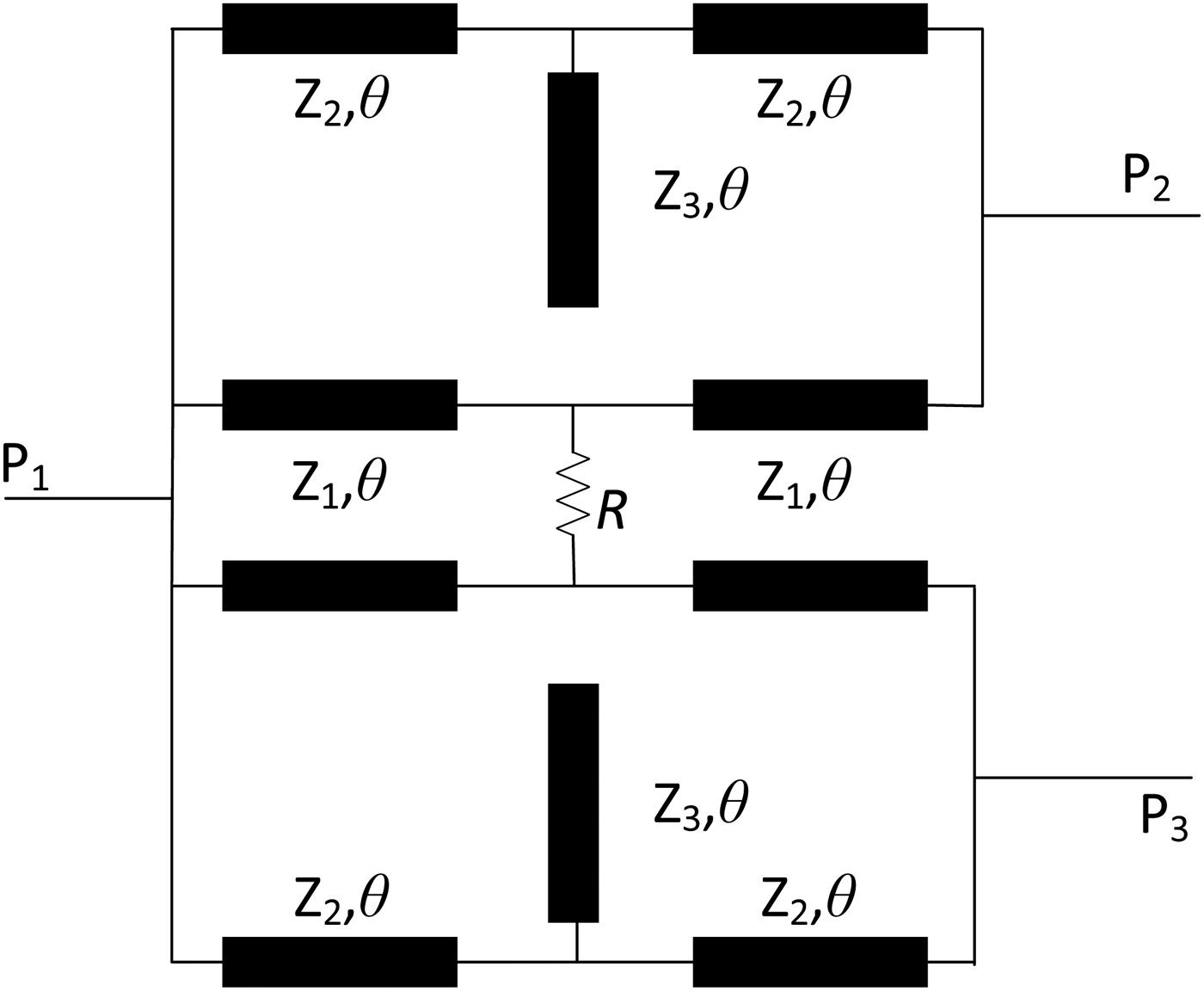
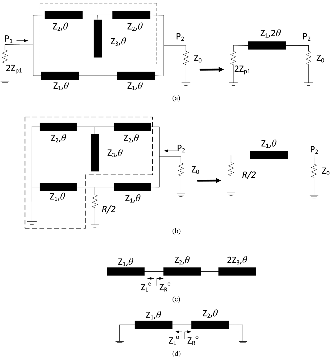
The schematic of the power divider is shown in Fig. 1. It is based on two stepped impedance ring resonators and one resistor. Zi (i = 1, 2, 3) is the characteristic impedance of each transmission line section. All the transmission lines have the same electrical length of θ which is one quarter of the wavelength specified at the central frequency. Since the power divider is symmetrical, so the even- and odd-mode method can be used to analysis the circuit. When the power divider is under even-mode, the symmetrical plane is magnetic wall. The whole circuit can be symmetrical bisected. Looking from port 1, the circuit in the dash line is open since the electrical length of the transmission lines are 90°. So the circuit can be simplified as depicted in Fig. 2(a). Assuming perfect impedance matching is achieved, the following equations can be obtained.
 $${Z_1} = {Z_0},$$
 $${{\rm Z}_{{\rm p}1}} = \displaystyle{{{Z_0}} \over 2},$$
when the power divider in Fig. 1 is under odd-mode excitation, the voltage along the symmetrical plane is zero. We can bisect the circuit by grounding the symmetrical plane. Looking from port 2, the circuit in the dash line is open because the electrical length of transmission is 90°. So the circuit can be simplified as depicted in Fig. 2(b). To achieve impedance matching, the following equation must be met.
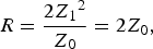 $$R = \displaystyle{{2{Z_1}^2} \over {{Z_0}}} = 2{Z_0},$$
Schematic of the proposed power divider.

(a) Equivalent even-mode circuit of the power divider (b) equivalent odd-mode circuit of the power divider (c) equivalent even-mode circuit of the circuit in (a) (d) equivalent odd-mode circuit of the circuit of the circuit in (a).
It can be found that Z 2 and Z 3 have no influence on the matching of port 1, but the transmission poles and zeroes are affected by them. The circuit in Fig. 2(a) is a filter, the transmission poles can be determined if the circuit is excited by the even- and odd-mode sources, respectively.
In the even mode case, the open stub is divided in half along the symmetrical plane so the characteristic impedance is 2Z 3, as shown in Fig. 2(c). The resonance frequencies can be derived and it can be simply expressed as follows [Reference Sun and Zhu10]:
 $${{\rm Z}_L}^e + {{\rm Z}_R}^e = 0,$$
where
 $${{\rm Z}_L}^e = \displaystyle{{{Z_1}} \over {j\tan \theta}},$$
 $${{\rm Z}_R}^e = j{{\rm Z}_{\rm 2}}\displaystyle{{{R_Z}\tan \theta - 2{R_S}\cot \theta} \over {{R_Z} + 2{R_S}}},$$
 $${R_Z} = \displaystyle{{{{\rm Z}_{\rm 2}}} \over {{{\rm Z}_{\rm 1}}}},$$
 $${R_S} = \displaystyle{{{{\rm Z}_{\rm 3}}} \over {{{\rm Z}_{\rm 1}}}}.$$
In the odd mode case, the open stub is shorted; the equivalent circuit is shown in Fig. 2(d). The resonance frequencies can be obtained and can be expressed as [Reference Sun and Zhu10]:
 $${\rm Z}_L^o + Z_R^o = 0,$$
where
 $${Z_L}^o = j{Z_1}\tan \theta,$$
 $${Z_R}^o = j{Z_2}\tan \theta.$$
Based on the transmission line theory described in [Reference Matsuo, Yabuki and Makimoto9, Reference Sun and Zhu10], the transmission zeroes can be obtained when Y 21 = Y 12 = 0, where the Y-parameters are the admittance matrices of the two propagation paths between port 1 and 2 in Fig. 2(a), such that
 $$\sin 2\theta + 2{R_Z}\sin \theta \cos \theta - \displaystyle{{{R_Z}^2} \over {{R_S}}}{\sin ^2}\theta \tan \theta = 0$$
According to the analysis above, all the even- and odd-mode resonant frequencies and transmission zeroes of the ring can be calculated by (4)–(12). Figure 3 plots the first three normalized resonant frequencies f o1/f o1, f e1/f o1, f e2/f o1 and first two normalized transmission zeroes f z1/f o1, f z2/f o1 versus R Z under different values of R S. f o1 is the first resonant frequency when the resonator in Fig. 2(a) is excited by the odd-mode source.
Normalized resonant frequencies and transmission zeroes versus RZ under different values of R S.
As depicted in Fig. 3, the three resonant frequencies are distributed in the range of the two transmission zeroes and the transmission zeroes are very close to the even-mode resonant frequencies, this means the roll-off skirts near the cut-off frequencies are very sharpe. It can be obtained when R Z is fixed, the smaller the R S is, the bigger is f e2/f o1 − f e1/f o1. When R S is fixed, the bigger the R Z is, the bigger is f e2/f o1 − f e1/f o1. These characteristics of the ring resonator can be applied to design a wideband filter with good selectivity.
B) Design of interdigital-coupled feed lines
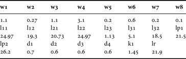
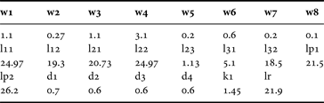
To achieve a bandpass response and suppress the second harmonic, three interdigital-coupled lines are applied at the input port and output ports. As depicted in (2), the input impedance of the circuit under the even-mode excitation equals to Z 0, so the input impedance of the whole circuit under even-mode excitation is Z 0/2. To realize good impedance matching at port 1, an impedance transition from Z 0 to Z 0/2 need to be designed. The layout and dimensions of the ports are shown in Fig. 7 and Table 1, respectively. The length of interdigital-coupled feed line is about quarter-wavelength at the central frequency f 0. According to the analysis in [Reference Sun and Zhu27], by adjusting the length of the interdigital-coupled feed line, the first harmonic of the stepped ring resonator can be suppressed and the stopband can be improved. A commercial software HFSS is used in this design and the simulated results of the interdigital-coupled lines are shown in Fig. 4.
(a) Simulated results of port 1 (b) simulated results of port 2
Physical dimensions of the fabricated power (unit: mm).
C) Design procedure of the power divider
Z 1 and R can be calculated by (1) and (3). But there are not explicit design equations to calculate Z 2 and Z 3. We can estimate their values according to Fig. 3 if the fractional bandwidth is given. The design procedure of the power divider is given as follows:
(1) Calculate Z 1 and R according to (1) and (3).
(2) According to the given fractional bandwidth, estimate their approximate values of R Z and R S in Fig. 3. Maybe there are several combination values with the same bandwidth, choose the proper one.
(3) Design the input and output interdigital-coupled feed lines. Tune the length of interdigital-coupled feed lines to suppress the harmonic frequency.
(4) Integrate the two filters, input port and output port. The resistor is used as isolation element. Since the coupled-lines are connected to the ring resonator, the bandwidth will be widened. So we need to optimize the values of Z 2 and Z 3.
III. EXPERIMENTAL RESULTS
In order to investigate the effect of the fabrication tolerances on the RF performance of the proposed power divider, a power divider designed using ideal circuit elements is simulated. Z 1, Z 2, Z 3 and R are chosen as 50, 100, 50 and 100 Ω, respectively. The tolerance of the manufacturing process is 0.02 mm. The layout of the power divider is shown in Fig. 5 and the dimensions of the power divider are listed in Table 1. According to the simulated results by HFSS, the parameters l11, w1, l21, w2, l32, w3, lp1, lp2 are more sensitive to the response of the power divider than other parameters. Figure 6 shows the simulated results of the power divider versus variations in the parameters above with fixed R = 100 Ω. “B” represents the simulated results using the parameters listed in Table 1. “A” represents the simulated results with 0.05 and 0.2 mm decrease in w1, w2, w3 and l11, l21, l32, lp1, lp2. “C” represents the simulated results with 0.05 and 0.2 mm increase in w1, w2, w3 and l11, l21, l32, lp1, lp2. The simulated frequency responses of the power divider versus R (±10%) with fixed Z 1 = 50 Ω, Z 2 = 100 Ω, Z 3 = 50 Ω are shown in Fig. 7.
Layout and photograph of the fabricated power divider.
(a)Simulated results of S 21and S 11 (b) simulated results of S 22 and S 33. ‘A’ represents the simulated results with 0.05 and 0.2 mm decrease in w1, w2, w3 and l11, l21, l32, lp1, lp2. ‘B’ represents the simulated results using the parameters listed in Table 1. ‘C’ represents the simulated results with 0.05 and 0.2 mm increase in w1, w2, w3, and l11, l21, l32, lp1, lp2.
(a) Simulated S 21 and S 23 (b) simulated S 11 and S 22
In Fig. 6, when the widths and lengths of the transmission lines decrease, the operating band shifts upward. This is because the corresponding operating central frequency increases when the lengths of the transmission line decrease. On the contrary, the corresponding operating central frequency decreases when the lengths of the transmission line increase. In Fig. 7, the operating band almost unchanges when the value of R changes, this is because the resistor is irrelevant with the bandwidth of the power divider, as analyzed above. In a word, the performance of the proposed power divider is not severely affected by the tolerance of the manufacturing process.
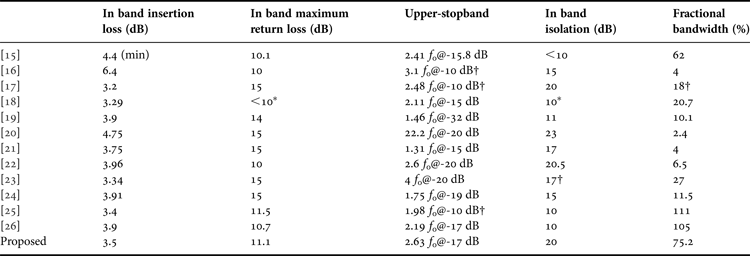
To validate the proposal, a power divider is designed and fabricated on a RF-35 substrate. The data of the substrate are ε r = 3.5, tanδ = 0.003, thickness of the dielectric layer is 0.508 mm, and the conductor thickness is 0.018 mm. The characteristic impedances of the transmission line in this design are Z 1 = 50 Ω, Z 2 = 100 Ω, Z 3 = 50 Ω. One of the pictures of the fabricated power divider is shown in Fig. 5. Figure 8 shows the simulated and measured results. There are in good agreement between the simulated and measurement results. The measured return loss is greater than 11.1 dB and the insertion loss is less than 4.1 dB in the pass band ranges from 1.27 to 2.8 GHz, with 75.2% fractional bandwidth. The bandpass bandedges’ skirts of the insertion loss are sharpened by the two transmission zeroes located at 1.16 and 2.9 GHz. The measured upper-stopband rejection is better than 16 dB from 3.1 to 5.3 GHz. The isolation in the passband is higher than 20 dB. Comparisons between the proposed and the previous ones are listed in Table 2. It can be found that the proposed one has much wider operating bandwidth than the ones in [Reference Gao, Sun and Xiao15–Reference Wang, Zhang and Hu24]. Although the power divider in [Reference Wong and Zhu25, Reference Song and Xue26] has wider operating bandwidth than the proposed one, the isolation in band are bad. The proposed circuit has wider upper stop band compared with [Reference Gao, Sun and Xiao15, Reference Singh, Basu and Wang17, Reference Cheong, Lai and Tam18, Reference Ren, Song, Hu and Chen21, Reference Wong and Zhu25, Reference Song and Xue26] and better performance on in band isolation compared with [Reference Gao, Sun and Xiao15, Reference Shao, Huang and Pang16, Reference Cheong, Lai and Tam18, Reference Li, Xue and Zhang19, Reference Ren, Song, Hu and Chen21, Reference Mirzavand, Honari, Abdipour and Moradi23–Reference Song and Xue26].
Simulated and measured results. (a) S 11 and S 21. (b) S 22 and S 23.
Comparisons between the proposed power divider and the reported ones.
* Estimate value.
† Simulation value.
IV. CONCLUSION
A power divider which has the dual function of power splitting and filtering embedded with two filters and one resistor is presented in this paper. The filter is based on stepped impedance ring resonator. Transmission-line theory is employed to obtain the even- and odd-mode resonant frequencies and transmission zeroes of the stepped impedance ring resonator. In order to achieve a bandpass response and suppress the second harmonic, three interdigital-coupled lines are applied at the input port and output ports. A sample operating at the central frequency of 2 GHz is fabricated and tested to validate the proposed idea. The measured results show the power divider has good performance on impedance matching, frequency selectivity, and isolation over the operating band. Later on, much effort will be made to miniaturize the size and extend the upper-stopband.
Cong Tang was born in Shangqiu, Henan Province, China, in 1987. He received the B.S. degree in Electronic Engineering from PLA Information Engineering University, Zhengzhou, China in 2010, and is presently working toward the Ph.D. degree at the UESTC (University of Electronic Science and Technology of China), Chengdu, China. His research interests include millimeter wave and microwave devices, circuits and systems.
Xian Qi Lin was born in Zhejiang Province, China, on July 9, 1980. He received the B.S. degree in Electronic Engineering from UESTC (University of Electronic Science and Technology of China), Chengdu, China, in 2003, and Ph.D. degree in Electromagnetic and Microwave Technology from Southeast University, Nanjing, China, in 2008. He joined the Department of Microwave Engineering at UESTC in August 2008, and became an Associate Professor and a Doctoral Supervisor in July 2009 and December 2011, respectively. From September 2011 to September 2012, he was a postdoctoral researcher in the Department of Electromagnetic Engineering at Royal Institute of Technology (KTH), Stockholm, Sweden. He has authored over 10 patents, over 40 scientific journal papers, and has presented over 20 conference papers. His research interests include microwave/millimeter wave circuits, metamaterials and antennas. Dr. Lin is a member of IEEE and a reviewer of many well-known journals such as IEEE-MTT/AP/MWCL/AWPL, JEMWA/PIER and EL. He was the recipient of 2011 honorable mention for the national hundred outstanding doctoral dissertations, a 2012 excellent young scholar presented by UESTC, and a 2013 new century excellent talent in University presented by Ministry of Education.
Yong Fan was born in 1963. He received the B.E. degree from Nanjing University of Science and Technology, Nanjing, Jiangsu, China, in 1985, and the M.S. degree from University of Electronic Science and Technology of China Chengdu, Sichuan China, in 1992. From 1985 to 1989, he was interested in microwave integrated circuits. Since 1989, He dedicated himself to researching and teaching on subjects of Electromagnetic Fields and Microwave Techniques for many years. His main research fields are as follows: electromagnetic theory, millimeter-wave communication, millimeter-wave, and terahertz circuits etc. Besides, he is interested in other subjects including broadband wireless access, automobile anti-collision, intelligent transportation intelligent transportation etc. He has authored and co-authored over 130 papers.
Kaijun Song (M'09-SM'12) received the M.S. degree in radio physics and the Ph.D. degree in Electromagnetic field and Microwave Technology from the University of Electronic Science and Technology of China (UESTC), Chengdu, China, in 2005 and 2007, respectively. Since 2007, he has been with the EHF Key Laboratory of Science, School of Electronic Engineering, UESTC, where he is presently a Full Professor. From 2007 to 2008, he was a postdoctoral research fellow with the Montana Tech of the University of Montana, Butte, USA, working on microwave/millimeter-wave circuits and microwave remote sensing technology. From 2008 to 2010, he was a research fellow with the State Key Laboratory of Millimeter Waves of China, Department of Electronic Engineering, City University of Hong Kong, on microwave/millimeter-wave power-combining technology and ultra-wideband (UWB) circuits. He was a senior visiting scholar with the State Key Laboratory of Millimeter Waves of China, Department of Electronic Engineering, City University of Hong Kong in November 2012. He has published more than 80 internationally refereed journal papers. His present research fields include microwave and millimeter-wave/THz power-combining technology; UWB circuits and technologies; microwave/millimeter-wave devices, circuits and systems; and microwave remote sensing technologies. Professor Song is the Reviewer of tens of international journals, including IEEE Transactions and IEEE Letters.