Introduction
Recently, the touch screen and display industry have begun to move to silver nanowire (AgNW)-based contacts due to their ability to readily integrate the contact with the lower-temperature and ink-based processing employed increasingly for the rest of the touch panel processing.[ 1 ] This has led to increased interest in the use of transparent nanowire contacts in other applications such as photovoltaics (PV), OLED/PLED, and Film Heaters. Their use in PV and especially PV produced on flexible substrates is very attractive due to their inherent flexibility and compatibility with roll-to-roll processing. Many recent reports have shown that AgNW transparent conductors (TCs) have excellent macroscopic optical transparency and electrical sheet resistance properties that are comparable with vacuum PVD-deposited Indium-Tin-Oxide (ITO) or ZnO transparent conductive oxides (TCOs) that are historically employed in these applications.[ Reference Woods, Wolk, Smith, Davande, Ribelin and Perkins 2 – Reference Guo and Ren 5 ] Nanowires alone cannot meet the increasingly demanding lifecycle for PV especially with some projections for device life of up to 50 years or for example the more stressful environment of hot and humid climates around the world. In particular, bare AgNW mesh TCs have significant problems with chemical reactivity,[ Reference Mayousse, Celle, Fraczkiewicz and Simonato 6 – Reference Hosseinzadeh Khaligh, Liew, Han, Abukhdeir and Goldthorpe 8 ] adhesion,[ Reference Aggarwal, van Hest, Perkins and Ginley 9 – Reference Chen, Lan, Wang, Zhu, Yang, Ding, Tang, Wang, Su and Xie 11 ] and shunting[ Reference Angmo, Andersen, Bentzen, Helgesen, Søndergaard, Jørgensen, Carlé, Bundgaard and Krebs 12 ] (i.e., reliability), as well as efficient photocurrent collection from the large open areas between the wires[ Reference Duan, Duan, Chen, Tao, Yang and Zhao 13 , Reference Zilberberg, Gasse, Pagui, Polywka, Behrendt, Trost, Heiderhoff, Goerrn and Riedl 14 ] and band energy alignment[ Reference Chang, Chiang, Kang, Chi, Chang, Wu and Lin 15 – Reference Shin, Kim, Ahn and Han 17 ] (i.e., efficiency). These problems in principle can be avoided by encapsulating the nanowires in a media that adheres better to the substrate, and protects the nanowires especially if the encapsulant has some moderate conductivity itself to minimize spreading loss. Composite contacts can be nearly ideally formed using an existing TCO and the AgNW mesh TC (c-TC). If properly chosen, the composite can adhere better and have improved band matching, comparable conductivity, and transparency to the nanowires themselves. Furthermore, such c-TCs can be fully atmospheric-pressure processible thereby reducing thermal budget and processing cost relative to conventional vacuum (sputter)-deposited TCO contacts. Additionally, it is enabling for high-throughput roll-to-roll processing. All of this can have a significant impact on the overall module cost for PV.
In this paper, we discuss recent results for nanowire composites deposited using solution-based ZnO from diethyl zinc (DEZ) precursors and radiofrequency (RF) sputtering combined with a number of commercial AgNWs of various aspect ratios and concentrations. We note that we also explored Zn acetate precursors, but the much higher decomposition temperature >300 °C is not compatible with many of the applications; so for the present study we focused on the DEZ where the decomposition temperature is ~120 °C. We show that the assumptions above can be readily realized in this fashion and we have produced high-performance c-TC by spin coating and by blade coating with TCO encapsulated nanowires having <10 Ω/sq and >90% transmittance.
Experimental
Spin coating
Glass substrates Corning E2K and Corning Willow glass were cut in 1 × 1 inch2 samples and were cleaned by sonicating in acetone for 15 min followed by sonication in isopropyl-alcohol for 15 min. Then substrates were dried with an N2 stream. The cleaned substrates were then further treated with UV plasma immediately before use.
Spin coating of base ZnO layer: The bottom ZnO layers were deposited from a mixture of one part 15 wt% DEZ in toluene to three parts tetrahydrofuran (THF) to achieve a 25 nm-thick film that was made fresh inside a dry-box prior to use. For each sample a volume of 300 µL was used for spin coating. For these films the spin rate was 3000 rpm with a ramp rate of 1000 rpm/s. The total spin time was 30 s and the films were subsequently annealed, on a hot plate in air, at 120 °C for 10 min.
Step-2: spin coating of AgNW
AgNW [diam. × length 35 nm (±5 nm) × 25 µm (±5 µm) from Sigma Aldrich, 5 mg/mL in ethanol] was used to form nanometal networks of varying surface coverage. The nanowires were spin-coated onto the previously spin-coated ZnO-coated glass substrate at 800–3000 rpm for 50 s. The volume of solution used for each sample was 250 µL. Coverage was evaluated as a function of spin rate from 250 to 1000 rpm.
Step-3: spin-coating ZnO for top encapsulant layer
As with the bottom ZnO layers the top layers were deposited from a mixture of one part 15 wt% DEZ in toluene to three parts THF to achieve a 50 nm-thick top layer. The volume of 300 µL was used for spin coating. These ZnO films were deposited with a spin rate of 3000 rpm with a ramp rate of 1000 rpm/s. The total spin time again was 30 s and the films were subsequently annealed in air at 120 °C for 10 min.
Sputtered ZnO films
Composites were also explored by sputtering the ZnO from an intrinsic ZnO (i-ZnO) target, similar to what is used for the i-ZnO window layer in a standard i-ZnO/TCO TC bilayer for copper indium gallium selenide (CIGS) cell fabrication. The ZnO film was sputtered using an RF magnetron at a power of 40 W RF, an Ar flow of 10 sccm Ar/O2 (1.5% O2 in Ar) flow of 10 sccm and a working pressure of 5 mTorr. Typical to what is used for CIGS cell fabrication. The overcoat was sputtered under the same conditions.
Blade coating
The fabrication of transparent conductor having structure ZnO/AgNW/ZnO was also explored using a blade coater capable of large-area deposition (Zehntner blade on a Coatema Easycoater). Coating was performed at room temperature. The gap between blade and glass substrate was kept at ~10 µm along with speed of blade of 1 m/min. The speed was chosen to achieve the desired coating thickness approximately the same as that for the spin-coated samples. The cleaned E2K glass was coated with DEZ and annealed at 120 °C. On top of the ZnO-coated glass, AgNW [diam. × length 35 nm (±5 nm) × 25 µm (±5 µm), 5 mg/mL in ethanol] was coated using two orthogonal passes to minimize texturing effects and subsequently annealed at 200 °C for bonding of nanowires, which decreases[ Reference Perkins, Aggarwal, van Hest, Gennett and Ginley 18 ] the contact resistance between wires. Overcoating of ZnO was done to improve the mechanical and chemical properties and had very little effect on sheet resistance and total transmittance. Willow glass samples were deposited on identically and produced very similar results.
The sheet resistance is measured using the four-point probe method. Optical spectra of the total transmission of films including diffuse were measured using a Varian Cary 5000 UV/VIS spectrometer with an integrating sphere. Therefore, the measured transmittance values include Fresnel reflection and scattered light. Optical specular transmittance of the films was measured using an Ocean Optics USB4000-VIS-NIR spectrometer coupled with fiber optics with a scanning stage that could automatically sample points across the surface of the sample. A bare glass substrate was used as a reference in the transmittance measurements. For all data shown, transmission values are corrected for the substrate.
Optical microscope images as well as scanning electron microscope (SEM) images were taken to investigate surface morphology and structural features of bare AgNW and AgNW/ZnO films.
Results and discussion
Pure nanowires: The original work utilized Blue Nanowires with a diameter of 90 nm approximately 30 µm long and wire with a diameter of 35 nm approximately 20 µm long. The work showed that the most desirable configuration for the wires is a small diameter and longer length. Unfortunately, Blue Nano was unable to supply subsequent batches of nanowires and we standardized on Sigma Aldrich nanowires (739448 ALDRICH) that are 115 nm in diameter and have lengths of 20–50 µm. These produced comparable results to the wires from Blue Nano. We believe that there is considerable additional optimization possible in the nanowire configuration.
Samples were blade and spin coated to explore the process dependence for both the ZnO layers and the AgNW density and interconnectivity. Table I summarizes the spin-coating data for samples deposited in a range of spin rates. While the films at 750 rpm were the most conductive all of the films were as good as or better than typical commercial ITO with similar light transmission, which typically has 15–75 Ω/sq.
Effect of spin speed on composite TC properties.

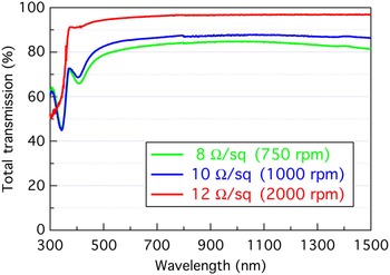
Table II shows a summary of the data for the spin-coated films using the same spin rate (750 rpm) but different nanowire concentrations. Figure 1 shows the morphology of the three films in Table I and the final nanowire densities are comparable, but might show a small decrease from S1 to S3. Figure 1 shows top-down SEM images of the deposited wires. The black bar below the picture indicates the scale bar, which was 20–30 µm for all films. As can be seen, the average wire length was between 50 and 75 µm, slightly longer than the specification. The films strongly adhered to the ZnO-coated substrate and were very robust after applying the ZnO overcoat. All films passed tape and scratch tests. More detailed mechanical testing is underway. The optical transmission data for these films are shown in Fig. 2 and demonstrate a very flat response from 300 to 1500 nm with transparency between 85% and 95% with the highest transmission observed for the films spun at the highest rpm. This co-aligns with the SEM images showing a lower nanowire density for those samples.
SEM images of nanowires spun on the ZnO-coated substrate with the different nanowire concentrations left to right (750, 1000, 2000 RPM).

Optical transmission of spin-coated c-TCs as a function of spin rate.

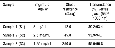
Effect of nanowire concentration on spin-coated c-TCs.
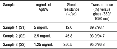
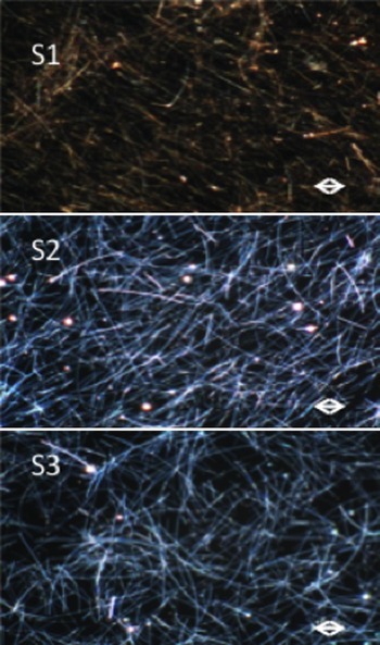
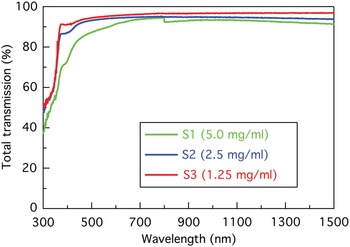
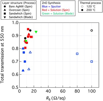
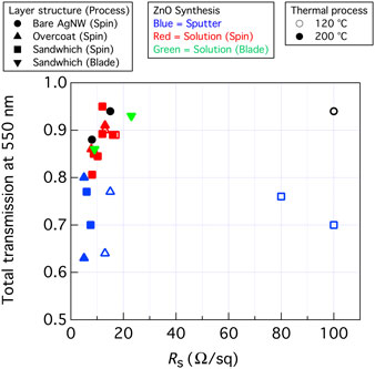
The samples with variable nanowire concentrations but the same spin rate (see Table II) show, not too surprisingly, that there is a clear decrease in the sheet resistance and a small decrease in the transmission with increasing silver wire content. The morphology of these films is shown in Fig. 3. The scale bar for all images is 10 µm. As can be seen, the average wire length was again ~50 µm. The transmittance measurements are shown for the whole spectrum in Fig. 4, and for two fixed wavelengths in Table II. As can be seen in Fig. 4, the optical transmission for S1, S2, and S3 has a relatively flat response from below 400 to over 1500 nm. There is some fall off at lower wavelengths for S1, which might be expected given the high nanowire density; however, the overall transmission is still quite good being on average 90% or higher. The flat spectral response is highly desirable for PV applications enabling more light absorption and thereby higher efficiencies. This much flatter response in the near-IR is due to the fact that the carrier concentration of the metal oxide matrix material is sufficiently low such that the carrier absorption and reflection, if any, is shifted to much lower photon energies farther out in the IR.[ Reference Ginley, Perkins, Ginley, Hosono and Paine 19 ] For a typical thin-film solar cell material such as CIGS this added transparency in the IR can yield up to 2% net efficiency. These data in both sets of experiments support that the ZnO bilayer does not substantially affect the overall conductivity or transmission. In fact, it may actually improve the interconnection between the wires somewhat by bonding the wires with moderately conductive oxide glue. If the conductivity of the oxide is high enough, then it is not necessary to bond the wires with the 200 °C anneal. Interestingly sputtered ZnO films do not behave comparably and in fact they show less adhesion than the solution-processed ones and do not pass the “tape” test, while the solution-processed ones do and are very robust. It is interesting to note that films where the wires are annealed and overcoated, or in the reverse order, are very comparable for the solution-processed films, but not for the sputtered films where the overcoat and annealed films are a factor of 2 less conductive than the ones that are annealed and overcoated. This seems to support a benefit to the solution-based precursor having some surface reaction with the Ag. This could be further modified through addition of ligands to the precursor ink. The film can also be intentionally doped to produce and even more ohmic contact. A summary of the data is shown in Fig. 5 where the red points are for the solution deposited films for bare nanowires and nanowire composites by spin and blade coating. The blue points are for the sputtered bottom films that then have a solution top coat. Note that the solution-deposited ZnO films behave nearly identical to the bare nanowires, while the sputtered films are nearly as conductive but far less transmissive.
Images of spin-coated c-TCs made with differing AgNW concentrations (see Table II).

Optical transmission spectra for spin-coated c-TCs made with differing AgNW concentrations (see Table II).

Summary of transmission and sheet resistance for AgNW/ZnO c-TCs.

Blade coating of films
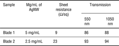
Spin coating is not amenable to large-area coating, so to explore the scalability of the approach films were blade coated. To avoid any unintentional texturing of the films due to the blade direction the films were coated twice in perpendicular directions. These films were overcoated with ZnO as above. Table III and Fig. 5 show the results of the blade coating.
Blade-coated c-TCs.
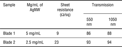
These results show that while the coating dynamics are very different the overall results are comparable. This is encouraging for the application of nanowire composite electrodes to large-scale roll-to-roll coating processes. To this end, we also coated Corning 100 µm-thick Willow glass, which is capable of being processed roll to roll and is therefore enabling for thin-film PV flexible modules. A previous work by Yang and co-workers has shown that a composite structures such as made here can significantly improve the mechanical stability of the TC especially to flexing, etc.[ Reference Song, Rim, Liu, Bob, Ye, Hsieh and Yang 16 ] Their use of TiO2 accomplished this, but could not help the conductivity or band edge alignment the same as a weakly doped TCO in the composite.
Benefits of solution-processible large-area nanowires
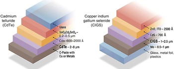
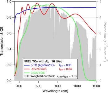
The potential benefit of c-TC to thin-film PV are multiple and co-aligned with the goals of lower-cost high-performance modules. Figure 6 shows a schematic for both a cadmium telluride (CdTe) and a CIGS thin-film solar cell. Integration in the case of CIGS is very facile simply replacing the ZnO/ITO layers with a ZnO or other TCO nanowire composite could improve band match, stability, and performance. In the CdTe case, it would have to be shown that if the back contact is replaces the oxide nanowire composite could take the ~600 °C processing temperatures. It is also potentially possible to replace the current opaque contact with a nanowire composite to create a bifacial cell. Given this and the fact that AgNW/ZnO c-TCs have demonstrated increased integrated photon flux compared with the standard TCO TCs with the same sheet resistance due to the higher IR transmissivity, leads directly to improved efficiency and further, by a judicious choice of oxide, the overall durability can likely be improved as well. In addition, due to the 100× higher conductivity of silver compared with conventional TCOs, very little silver is needed to achieve comparable sheet resistances, only 0.05 g/m2 to make a 15 Ω/sq corresponding to $0.05/m2 in the raw silver material. Further, the use of non-vacuum deposition methods to deposit the transparent conducting contact layer has the potential to reduce manufacturing costs by $2–$3/m2 compared with the use of conventional TCOs deposited by vacuum sputtering. This is based on the NREL analysis of the cost of sputter-deposited TCOs (both ZnO and ITO) compared with solution-deposited carbon nanotubes.[ Reference Bergeson 20 ] The biggest cost reduction comes from the great reduction in the capital equipment to <$0.10/m2 when no vacuum deposition equipment is required. Then further considering the materials costs, one finds that solution-deposited AgNW-based TCs could have a total coating cost as low as $0.50–$0.75/m2 compared with ~$3.40/m2 for the vacuum-sputtered TCOs currently used in many PV technologies. In terms of $/Watt, a $2/m2 cost savings approximately the same as a 2% improvement in solar transparency (assuming a 20% cell efficiency and AM1.5 illumination) as shown in Fig. 7, c-TCs can actually have improved net transparency due to their flat spectral response. This indicates that at parity with ITO there is a significant benefit but that the net result may be even larger. Looking beyond CIGS, PV application research in 2015 using c-TCs includes top electrodes on wafer Si PV,[ Reference Göbelt, Keding, Schmitt, Hoffmann, Jäckle, Latzel, Radmilović, Radmilović, Spiecker and Christiansen 21 ] hybrid organic-silicon PV,[ Reference Spechler, Nagamatsu, Sturm and Arnold 22 ] OPV tandems,[ Reference Angmo, Andersen, Bentzen, Helgesen, Søndergaard, Jørgensen, Carlé, Bundgaard and Krebs 12 ] perovskites,[ Reference Kim, Lee, Kwon, Jung, Park, Jeong and Moon 23 ] and perovskite-based tandems.[ Reference Bailie, Christoforo, Mailoa, Bowring, Unger, Nguyen, Burschka, Pellet, Lee, Grätzel, Noufi, Buonassisi, Salleo and McGehee 24 ]
Schematics of CdTe and CIGS solar cell stacks.

Comparison of transmission spectra for sputtered ZnO and atmospheric pressure processed c-TC with QE spectrum for CIGS solar cell. Solar photon flux is shown in gray versus right axis.

Conclusions
In this work, we show how scalable processing of large-area AgNW composites with TCOs can result in a synergistic improvement of performance, processing, and cost. While not fully optimized the nanowire composites show performance 10 Ω/sq and 90% transmittance of the best TCOs in use commercially. It was found that unlike the pure TCOs the solution processing of the nanowire composites produced higher performing more robust composites. Their ready scalability and low capital cost make them attractive for integration into large-area opto-electronics such as PV. The inherent robustness of essentially a fiber reinforces composite make them attractive for flexible applications as well.
Acknowledgments
This work was supported as part of the SunShot Initiative by the US Department of Energy, Office of Energy Efficiency and Renewable Energy, Office of Solar Energy Technology under Award Number DE-AC36-08GO28308 to the National Renewable Energy Laboratory (NREL). This research is based upon work supported in part by the Solar Energy Research Institute for India and the U.S. (SERIIUS) funded jointly by the U.S. Department of Energy subcontract DE AC36-08G028308 (Office of Science, Office of Basic Energy Sciences, and Energy Efficiency and Renewable Energy, Solar Energy Technology Program, with support from the Office of International Affairs) and the Government of India subcontract IUSSTF/JCERDC-SERIIUS/2012 dated 22nd Nov. 2012. Shruti Aggarwal would like to acknowledge the support of the Baskara Fellowship and Rajiv Singh would like to acknowledge the support of the Raman Fellowship.