
I. INTRODUCTION
Silicon (Si) is regarded as a unifying material for integrated circuits not only for electronics but also for photonics. This is due to the fact that Si is the second most abundant element (after oxygen) in the earth’s crust and hence the cost of producing high quality Si substrates is low. Furthermore, stable oxide, good mechanical robustness, high thermal conductivity, and large area are the merits of Si substrates. Most importantly, Si complementary metal oxide semiconductor (Si-CMOS) is the most mature, high yield, low cost, highly integratable, and scalable technology in the electronic industry. Reference Sze and Lee1–Reference Taur and Ning9
Si photonics, on the other hand, has been widely studied for shorter-reach optical interconnects such as chip-to-chip, board-to-board, and rack-to-rack communication as well as intrachip/intercore communication in the micro-processing unit (MPU). 10 This is to address the needs of an energy efficient and a high bandwidth data transmission with a high data processing rate on a single microchip. Reference Lannoo11–Reference Kirchain and Kimerling15 To realize a mass production scale, Si photonics have to leverage on the well-established Si-CMOS technology and business model to achieve a fully monolithic integrated Si-based photonic–electronic systems.
Most of the passive Si photonic devices, such as waveguides are based on Si. An Si waveguide with the dimension of a submicron has been monolithically integrated with Si-CMOS processes. Reference Tsybeskov, Lockwood and Ichikawa16 However, Si is not an ideal material, as active photonic components, for telecommunication, such as photodetectors, light sources, and electro-optical modulators. Engineering of defect states in Si has extended the Si photodetection to telecommunication wavelengths, but this approach suffers from a poor absorption coefficient and a trade-off in quantum efficiency. Reference Geis, Spector, Grein, Yoon, Lennon and Lyszczarz17,Reference Souhan, Grote, Driscoll, Lu, Stein, Bakhru and Osgood18 Modulators based on Mach–Zehnder interferometer have large footprints and high power consumptions. Reference Liu, Liao, Rubin, Nguyen, Ciftciogulu, Chetrit, Izhaky and Paniccia19,Reference Green, Rooks, Sekaric and Vlasov20 Si nanostructures have been investigated for light emission, but the electroluminescence (EL) efficiency is rather low especially at elevated injected current density (>1 mA/cm2). Reference Cheng, Anthony, Kortshagen and Holmes21 On the other hand, laser diodes (LDs) or light-emitting diodes (LEDs) based on III–V compound semiconductors are commercially available and are assembled onto Si photonic circuits using flip-chip bonding or a solder-based assembly. Reference Zimmermann22–Reference Lee, Liu and Seeds28 The light from a LD propagates through optical fiber and it is then coupled to a Si waveguide based on certain coupling mechanisms. Reference Gunn29 The problem of this scheme is that the form factor of the final chip is large and the power consumption is high. It is possible to integrate LDs or LEDs monolithically on the Si substrate through a thick graded buffer or wafer bonding technique, but cross-contamination of III–V elements to Si-CMOS processing tools cannot be avoided, and the process throughput is low. Reference Lee, Bao, Fitzgerald and Tan30,Reference Lee, Bao, Zhang, Kohen, Fitzgerald and Tan31
Germanium (Ge) is a promising material as it is compatible with CMOS processing. Reference Wada and Kimerling32 The direct bandgap of Ge is around 0.8 eV (which is equivalent to 1550 nm in wavelength). Reference Newman33,Reference Hayne34 Ge has been utilized in CMOS processing for strain engineering at the source and drain regions of MOSFET. Reference Zhang, Huang, Wu, Chen, Hong, Bera and Zhu35–Reference Feng, Thareja, Kobayashi, Chen, Poon, Bai, Griffin, Wong, Nishi and Plummer37 In addition, a Ge-on-Si photodetector is the most mature Si photonic component available in commercial products. In terms of light emitting, Ge has a pseudo-direct bandgap, (the difference between its direct bandgap at Γ valley and indirect bandgap at L valley is only 136 meV Reference Madelung38 ) and electrically pumped LDs have been demonstrated by several groups through band engineering. Reference Liu, Sun, Kimerling and Michel39–Reference Komiyama, Lizuka and Akasaka42
In this article, we report our approaches in achieving high quality Ge-on-Si (Ge/Si) substrates. The performance of various active photonic devices fabricated on these substrates are presented. Future work will be proposed to further improve the performance of the photonic devices. Finally, the potential applications of such integrated photonic devices with Si-CMOS will be discussed.
II. EPITAXIAL GROWTH OF Ge ON Si SUBSTRATE
A. Overview of epitaxy growth of Ge on Si substrate
Ge is a group IV material and it is located right below Si in the periodic table of elements. Ge exhibits several superior electrical and optical properties. In terms of electrical properties, Ge has a much higher carrier mobility than that of Si [electron mobility of Ge: 3900 cm2/(V∣s) versus Si: 1400 cm2/(V∣s); hole mobility of Ge: 1900 cm2/(V∣s) versus Si: 450 cm2/(V∣s)] and has been used for future p-channel MOSFETs. Reference Shang, Okorn-schimdt, Ott, Kozlowski, Steen, Jones, Wong and Hanesch43 Optically, Ge has a longer cut-off wavelength (∼1.55 µm) than that of Si, and thus Ge photodetectors can be operated between O- to U-bands of telecom wavelengths (1.27–1.67 µm). Reference Fathpour44 Due to its pseudo-bandgap behavior [small energy difference of 136 meV between the direct valley (Γ) and indirect valley (L)], an efficient light-emitting device becomes possible by engineering its band structure. Recently, a laser fabricated on a Ge/Si substrate has been demonstrated by Michel et al. Furthermore, Ge has a lattice constant that closely matches gallium arsenide (GaAs), and it can be used as a buffer layer for the growth of subsequent III–V compound semiconductors Reference Kohen, Bao, Lee, Lee, Tan, Yoon and Fitzgerald45,Reference Kohen, Nguyen, Yadav, Kumar, Made, Heidelberger, Gong, Lee, Lee, Yeo, Yoon and Fitzgerald46 Therefore, large scale III–V on-Si substrates can be realized.
On the flip side, the difference in lattice constant between Ge (a = 5.658 Å) and Si (a = 5.431 Å) is larger than desirable at about 4.18%. When a Ge film with thickness beyond its critical thickness is grown on top of an Si substrate, misfit dislocations are inevitably generated at the Ge/Si interface and are propagated toward the Ge surface as threading dislocations. These dislocations act as unfavourable generation/recombination centers for carriers and severely deteriorate the device performance especially for minority carrier devices, such as lasers, photodiodes, photovoltaics, heterojunction bipolar transistors (HBTs), etc. Furthermore, high surface roughness is also observed as the result of three-dimensional (3D) Stranski–Krastanov growth mode and this causes difficulties in subsequent epitaxial growth and process integration. These limitations have precluded the use of Ge/Si substrates in optoelectronic applications.
To achieve low threading dislocations and smooth surface of Ge/Si (001) substrates, various approaches have been proposed. The most common method is to grow a fully relaxed thick-graded Si x Ge1−x buffer layer to match the lattice constant between the Si substrate and the Ge epitaxial film. Since the lattice constant mismatch between the Si x Ge1−x and Ge is smaller than that of the Si and Ge and also because the surface energy of Si x Ge1−x is lower than that of Si, the Franck–van-der-Merwe growth mode is preferred in the Si x Ge1−x system. The compositional gradient of the graded buffer layer, grading rate, growth temperature, and conditions will contribute to final treading dislocation densities (TDD) and surface roughness of the Ge epitaxial film. Reference Fitzgerald, Xie, Green, Brasen, Kortan, Michel, Mi and Weir47,Reference Shah, Dobbie, Myronov and Leadley48 By inserting a chemical mechanical planarization (CMP) midway through the graded buffer growth, a low TDD of 2.1 × 10⁶/cm2 can be obtained. Reference Curie, Samvedam, Langdo, Leitz and Fitzgerald49 Another technique is by incorporating antimony (Sb) into the thick graded Si x Ge1−x buffer. This method achieves a very low TDD of 5.4 × 10⁵/cm2 and a low surface roughness of 3.5 nm. A monolayer of Sb is found to be effective in relieving the stress which is caused by the large lattice constant mismatch between Si and Ge. Reference Liu, Tong, Luo and Wang50 The graded buffer layer usually has a thickness of about 10 µm prior to the growth of pure Ge. Reference Luryi, Kastalsky and Bean51,Reference Curie, Samvedam, Langdo, Leitz and Fitzgerald52 Such thickness is impractical in industrial reduced pressure chemical vapor deposition tools, as growth occurs on one side only as such the wafer bow is prohibitive. Reference Hartmann, Sanchez, Van Den Daele, Abbadie, Baud, Truche, Augendre, Clavelier, Cherkashin, Hytch and Cristoloveanu53 Hence, it may be desirable to have thinner initial layers for some applications, e.g., laser, photovoltaic, etc. Reference Liu, Sun, Kimerling and Michel39,Reference Jain54 For this purpose, an ultrathin ∼10 nm of Si0.5Ge0.5 buffer layer is introduced before the Ge epitaxial films grown directly on Si substrates. The TDD of <1 × 10⁷/cm2 and smooth surfaces (RMS surface roughness of 0.44 nm) of Ge/Si substrates are reported. Reference Nakatsuru, Date, Mashiro and Ikemoto55
Selective area growth (SAG) or selective epitaxial growth technique is another approach to achieve low TDD of the Ge epitaxial films. This technique requires additional substrate patterning which is then followed by epitaxial lateral overgrowth. Mesas with dimensions of <40 µm and with an aspect ratio >1 are patterned through the lithography and etched through the SiO2 layer to reach the surface of the Si substrate. Ge epitaxial layers are therefore grown selectively on the patterned windows. Reference Langdo, Leitz, Curie and Fitzgerald56 As threading dislocations are not glided parallel to the growth directions, they can glide to the oxide sidewalls and annihilate. Reference Bai, Park, Cheng, Curtin, Adekore, Carroll and Lochtefeld57,Reference Ren, Rong, Kamins, Harris and Miller58 Hence, the SAG approach can eliminate defects originated from the Ge/Si interface in the growth windows and results in a very low TDD (<1 × 10⁶/cm2) in the upper part of the Ge films. Another similar technique is called aspect ratio trapping. Reference Fiorenza, Park, Hydrick, Li, Li, Curtin, Carroll and Lochtefeld59 Mesas with smaller dimension of <1 µm and higher aspect ratio of >2 are patterned on the SiO2 layer and are etched to reach the Si surface. Ge epilayers are subsequently grown selectively on the patterned windows. Low TDD (∼1 × 10⁶/cm2) of Ge films have been achieved by this technique.
A more practical approach from the manufacturing point of view is the two-step growth method. Reference Colace, Masini, Galluzzi, Assanto, Capellini, Gaspare, Palange and Evangelisti60–Reference Luan, Lim, Lee, Cheng, Sandland, Wada and Kimerling62 This approach consists of a low temperature (LT, 300–400 °C) growth step that is followed by a high temperature (HT, 600–850 °C) Ge growth. A thin Ge seed layer (30–100 nm) is grown at a low temperature to limit the mobility of Ge adatoms and hence prevent the 3D nucleation of Ge. After that, a thick Ge (to the desired thickness) film is grown at the high-temperature regime to achieve a higher growth rate and better Ge crystallinity. Additional annealing steps after the two-step growth approach are introduced to further reduce the TDD and smoothen the surface of the Ge epitaxial films. There are several annealing methods, including multiple hydrogen annealing Reference Nayfeh, Chui and Saraswat63 and thermal cyclic annealing. Reference Tan and Tan64
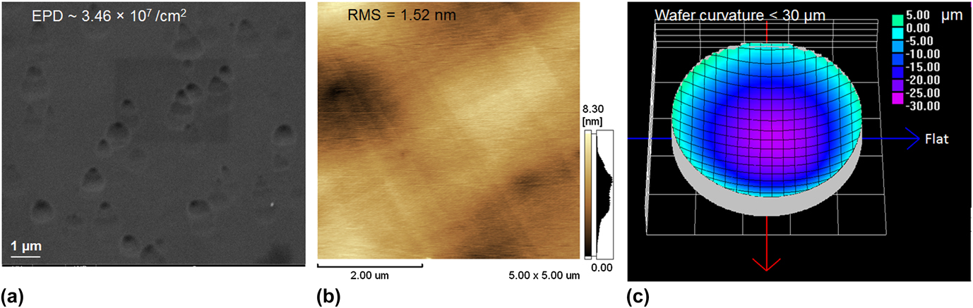
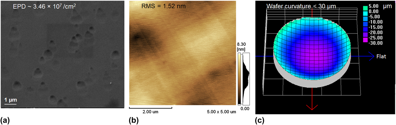
The authors’ group has reported Ge epitaxial films that were grown directly on Si (001) substrates by the two-step growth approach in metal–organic chemical vapor deposition combined with a thermal cyclic annealing process. A pure Ge seed layer with a thickness of 60 nm was grown at 350 °C. After that, the reactor temperature was increased to 650 °C and then 800 nm of HT Ge was grown on top of the Ge seed layer. Finally, thermal cyclic annealing was introduced to enhance the surface mobility of the Ge adatoms to control the surface roughness and to reduce TDD. One thermal cyclic annealing was performed in H2 ambient between 650 and 850 °C. TDD of the Ge film is 3.46 ± 0.37 × 10⁷/cm2 (Refs. Reference Lee, Tan, Jandl, Fitzgerald and Tan65 and Reference Lee, Jandl, Tan, Fitzgerald and Tan66) with an RMS surface roughness of ∼1–2 nm as shown in Figs. 1(a) and 1(b). In addition, Fig. 1(c) depicts that the wafer curvature of this 8ʺ Ge/Si substrate is <30 µm, (in term of absolute value) which can be handled by most of the processing tools such as the 8ʺ lithography stepper, as the stepper can handle the wafer with a wafer curvature within ±70 µm.
(a) Etch pit density (EPD) determination of a Ge epilayer that was grown directly on a Si substrate. (b) Two dimensional (2-D) AFM scans (dimension: 5 × 5 µm) shows the RMS surface roughness of the Ge epilayer on the Si substrate. The RMS roughness is 1.52 nm and clear cross-hatch patterns are observed. (c) Wafer curvature measurement on the Ge epilayer on the 200 mm Si wafer. The value is <30 µm (in absolute value).
B. Methods to achieve high crystalline quality Ge epitaxial film on Si substrate
Dislocations act as recombination centers for minority carriers; therefore, they play an important role in determining the performance of most of the minority carrier devices (e.g., laser, LEDs, HBTs, etc). Dislocations degrade the minority carrier lifetime and hence the carrier diffusion length as described in the following expressions Reference Masafumi, Chikara and Yoshio67,Reference Masafumi and Chikara68 :
 $${1 \over \tau } = {1 \over {{\tau _0}}} + {1 \over {{\tau _{{\rm{TDD}}}}}}\quad ,$$
 $${1 \over {{\tau _{{\rm{TDD}}}}}} = {{{\pi ^3}{D_{\rm{p}}}{N_{{\rm{TDD}}}}} \over 4}\quad ,$$
 $${D_{\rm{p}}} = {{7.347 \times {{10}^6}} \over {6.697 \times {{10}^5} + {n^{1{\rm{/}}3}}}}\quad ,$$
 $${1 \over {L_{\rm{p}}^2}} = {1 \over {{{\left( {6 \times {{10}^{ - 4}}} \right)}^2}}} + 3 \times {10^{ - 11}}n + {{{\pi ^3}{N_{{\rm{TDD}}}}} \over 4}\quad ,$$
where τ is the minority carrier lifetime, τ0 is the minority carrier lifetime without TDD given by the radiative lifetime, Reference Nayfeh, Chui and Saraswat63,Reference Tan and Tan64,Reference Ginige, Corbett, Modreanu, Barrett, Hilgarth, Isella, Chrastina and von Känel69 τTDD is the TDD-limited minority carrier lifetime, D p is the empirical minority carrier diffusion coefficient, N TDD is the threading dislocation density, L p is the diffusion length, and n is the doping concentration. The theoretical dependence of the minority carrier lifetime in n-GaAs on TDD can be determined based on Eqs. (1)–(3). Minority carrier lifetime decreases with increasing TDD, but it is reasonably high (∼10 ns) for device applications provided that the value of TDD is in the order of ∼106/cm2 and below. The lifetime is shortened drastically to 0.1 ns at a TDD of 5× 10⁷/cm2. Hence, there is a need to further reduce the TDD of the Ge epitaxial films.
In the authors’ group, two approaches were developed to reduce the TDD of the Ge film on Si substrates. The first approach is to fabricate and anneal a germanium-on-insulator (GOI) substrate at a high temperature in oxygen (O2) ambient. Reference Lee, Bao, Chong, Tan, Fitzgerald and Tan70,Reference Lee, Bao, Chong, Tan, Fitzgerald and Tan71 The second approach is to dope an LT Ge seed layer with a high concentration of arsenic (As) dopants. Reference Lee, Bao, Wang, Wang, Yoon, Michel, Fitzgerald and Tan72
The first approach is presented here. Firstly, SiO2 was deposited on the Ge/Si substrate (after the two-step growth approach and thermal cyclic annealing) by plasma-enhanced chemical vapor deposition (PECVD). The oxide surface was planarized by CMP to ensure that the RMS surface roughness is <1 nm, which is one of the most important criteria for a successful direct wafer bonding. The Ge/Si (after the PECVD oxide deposition and CMP) and a Si (001) handle wafer were subjected to O2 plasma exposure, followed by rinsing them with deionized water and then spin dried in a spin rinse dryer SRD. The two wafers were then bonded together at room temperature and at atmospheric pressure. Post-bonding annealing of the bonded wafer pair was carried out at 300 °C in atmospheric N2 ambient for 3 h to further enhance the bond strength. The Si substrate from the Ge/Si wafer was then removed by a combination of mechanical grinding and wet-etching in the tetramethylammonium hydroxide (TMAH) solution. Prior to wet-etching in TMAH, the backside of the Si handle was protected by a protective film, ProTEK®B3-25 (Brewer Science, Rolla, Missouri). The Ge epitaxial film acts as an etch-stop layer as the etching selectivity of Ge over Si is high (>1:100) in the TMAH solution. The etching was carried out at 80 °C until the Si was completely removed. The ProTEK®B3-25 protective coating was then removed in O2 plasma with a power of 800 W. The GOI substrate was then subjected to annealing between 700 and 850 °C in an O2 environment. After that, the sample was etched in HF solution (49% HF:H2O = 1:10, by volume) for 60 s to remove the oxidized Ge layer. Lastly, the sample was subjected to CMP process to smoothen the Ge surface which was roughened during the high-temperature annealing step.
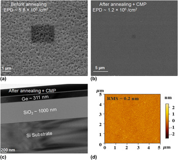
Etch pit density (EPD) method is used to reveal TDD of the Ge epitaxial films. As shown in Fig. 2(a), EPD of the GOI sample before O2 annealing is 5.26 ± 0.57 × 10⁸/cm2. TDD is reduced by more than two orders of magnitude to 1.2 ± 1.37 × 10⁶/cm2 after O2 annealing, as depicted in Fig. 2(b). The misfit dislocations which are previously confined along the Ge/Si interface are now exposed and accessible from the top. This provides the ease to remove the exposed misfit dislocations by either CMP or annealing process. After annealing, no misfit or treading dislocations are observed in the cross-sectional bright field transmission electron microscopy (X-TEM) as shown in Fig. 2(c), suggesting that TDD of the GOI sample is greatly reduced. O2 annealing is chosen because: (i) it oxidizes the Si/Ge intermixed layer and Ge layer to remove the misfit dislocations; (ii) the number of threading dislocations can be annihilated once the misfit dislocations are eliminated; and (iii) the high-temperature annealing can also recrystallize the Ge epitaxial film, which is similar to the recrystallization process of poly-Si to crystalline-Si. As shown in Fig. 2(d), the RMS surface roughness of the Ge epilayer after the CMP process is ∼0.2 nm and no cross-hatch patterns are observed, indicating that an effective CMP process is established.
EPD determination for (a) before annealing and (b) after O2 annealing of a GOI substrate. (c) Cross-sectional transmission electron microscopy (X-TEM) bright field image shows the overall view of the GOI substrate after subjected to O2 annealing and chemical mechanical planarization (CMP) processes. (d) Two dimensional (2-D) AFM scans (dimension: 5 × 5 µm) shows the RMS surface roughness of the GOI substrate after O2 annealing and CMP processes.

In the second approach, a LT Ge seed layer was grown and doped with a high concentration of As dopants (concentration of the As dopants ∼1019/cm3). After that, high-temperature Ge growth at 650 °C was carried out by gradually reducing the AsH3 flow from maximum flow (which can achieve As concentration of ∼1 × 10¹⁹/cm3) to zero and then was followed by pure Ge growth at 650 °C to achieve the intended thickness. Similar thermal cyclic annealing as mentioned previously was introduced to further reduce TDD and achieve a smooth Ge surface.
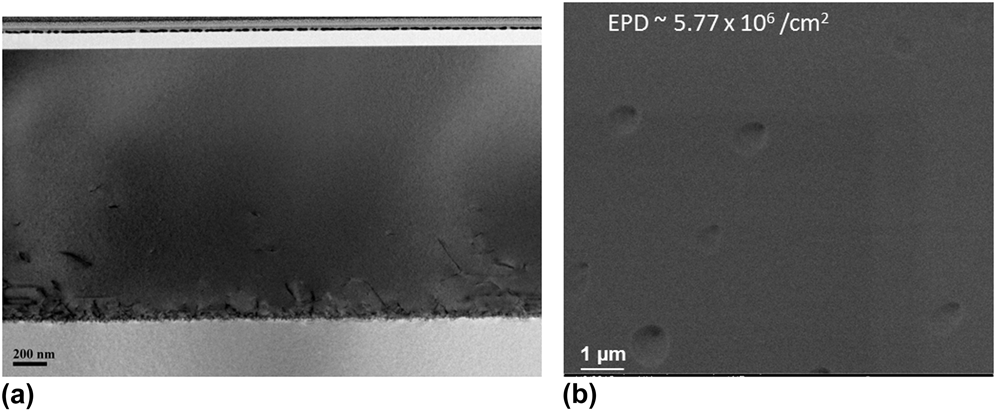
The X-TEM image in Fig. 3(a) shows that the Ge epitaxial layer has a thickness of ∼1.5 µm. The misfit dislocations are mostly confined along the Ge/Si regrowth interface as shown in the X-TEM image. In addition, most of the threading dislocations are confined within the first 700 nm Ge layers, (above the Ge/Si interface) where the Ge epilayer is doped with As during growth steps. Beyond this thickness, no visible threading dislocation is observed under X-TEM.
(a) X-TEM bright field image shows a Ge epitaxial film grown directly on a Si substrate using the heavily arsenic (As) doped Ge seed layer. The treading dislocations are confined within the first 700 nm of the Ge epilayer. Beyond this thickness, minimum number of dislocations are observed which indicates a high quality Ge film. (b) EPD determination of the Ge epilayer on the Si substrate.

EPD of the Ge epilayer with the As-doped Ge seed layer is 5.77 ± 0.74 × 10⁶/cm2 as shown in Fig. 3(b). This is about one-order of magnitude lower than that of the Ge/Si substrate using the intrinsic Ge seed layer. This observation is due to the role of As dopants in promoting Si/Ge interdiffusion that results in a gradual change in the composition of Si1−x Ge x . This behavior may contribute to the TDD reduction. Recently, it is reported that Si–Ge interdiffusivity can be enhanced by 10–20 times when the Ge is highly doped with phosphorus (P) due to a much faster P transport toward the Ge seeding layer which increases Si–Ge interdiffusion due to the Fermi-level effect. Reference Cai, Dong, Tan, Tan and Xia73 This work suggests that heavy levels of arsenic doping may also increase interdiffusion by a similar mechanism.
In addition, the RMS surface roughness of the Ge/Si substrate with a heavily As-doped seed layer is also much smaller, ∼0.37 nm. The smooth surface is a result of dislocation motions occurring after the completion of epitaxial growth. In addition, the As dopants may also help to promote the migration of Ge atoms during the high-temperature annealing which further improves the smoothness of the Ge epilayer. Reference Jung, Hsieh, Kwong, Liu and Brennan74
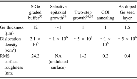
A comparison table which summarizes the quality of Ge epitaxial films on Si substrates using different approaches is shown in Table I.
A comparison table which summarizes the quality of Ge epitaxial films on Si substrates using different approaches.

III. Ge PHOTO-DETECTOR
Ge-on-Si photodetector (PD) is one of the most mature integrated Ge photonic devices. A p-i-n diode is the most commonly available structure. The key challenges to high-performance devices are optimization of the TDD and surface passivation technique. Higher TDD increases the dark current and poor surface passivation leads to higher surface recombination, which results in a further increase in the dark current. TDD can be controlled by graded Si x Ge1−x buffer layers. Huang et al. Reference Huang, Oh, Banerjee and Campbell75 have investigated the graded buffer technique and have successfully reduced the dark current density by one-order of magnitude. Through improvement in the surface passivation technique, the dark current density has been further reduced to 1 mA/cm2 at −1 V. Reference DiLello, Johnstone and Hoyt76
Thanks to the improvements in the Ge/Si epitaxial growth, Liu et al. reported high performance Ge vertical p-i-n Ge photodetectors that were directly grown on a p+-Si substrate. Reference Liu, Michel, Giziewicz, Pan, Wada, Cannon, Jongthammanurak, Danielson, Kimerling, Chen, Llday, Kartner and Yasaitis77,Reference Liu, Cannon, Wada, Ishikawa, Jongthammanurak, Danielson, Michel and Kimerling78 Dehlinger et al. Reference Dehlinger, Koester, Schaub, Chu, Quyang and Grill79 adopted a high quality Ge-on-SOI epitaxy followed by a lateral p-i-n configuration to improve the photodetector absorption efficiency and speed. To mitigate the trade-off between responsivity and bandwidth that these normal-incidence Ge photodetectors had, waveguide-integrated photodetectors were later developed, in which an Si (or SiN Reference Ahn, Hong, Liu, Giziewicz, Beals, Kimerling, Michel, Chen and Kartner80 ) waveguide was built Reference Vivien, Osmond, Fedeli, Marris-Morini, Crozat, Damlencourt, Cassan, Lecunff and Laval81–Reference Virot, Vivien, Fédéli, Bogumilowicz, Hartmann, Bœuf, Crozat, Marris-Morini and Cassan83 or evanescently-coupled Reference Yin, Cohen, Morse, Sarid, Chetrit, Rubin and Paniccia84 into an epitaxial-Ge waveguide structure on Si Reference Vivien, Polzer, Marris-Morini, Osmond, Hartmann, Crozat, Cassan, Kopp, Zimmermann and Fédéli85 or silicon-on-insulator (SOI). Reference Wang, Loh, Chua, Zang, Xiong, Loh, Yu, Lee, Lo and Kwong86 Both high responsivity (∼1 A/W) and high speed (>30 GHz) could be simultaneously achieved.
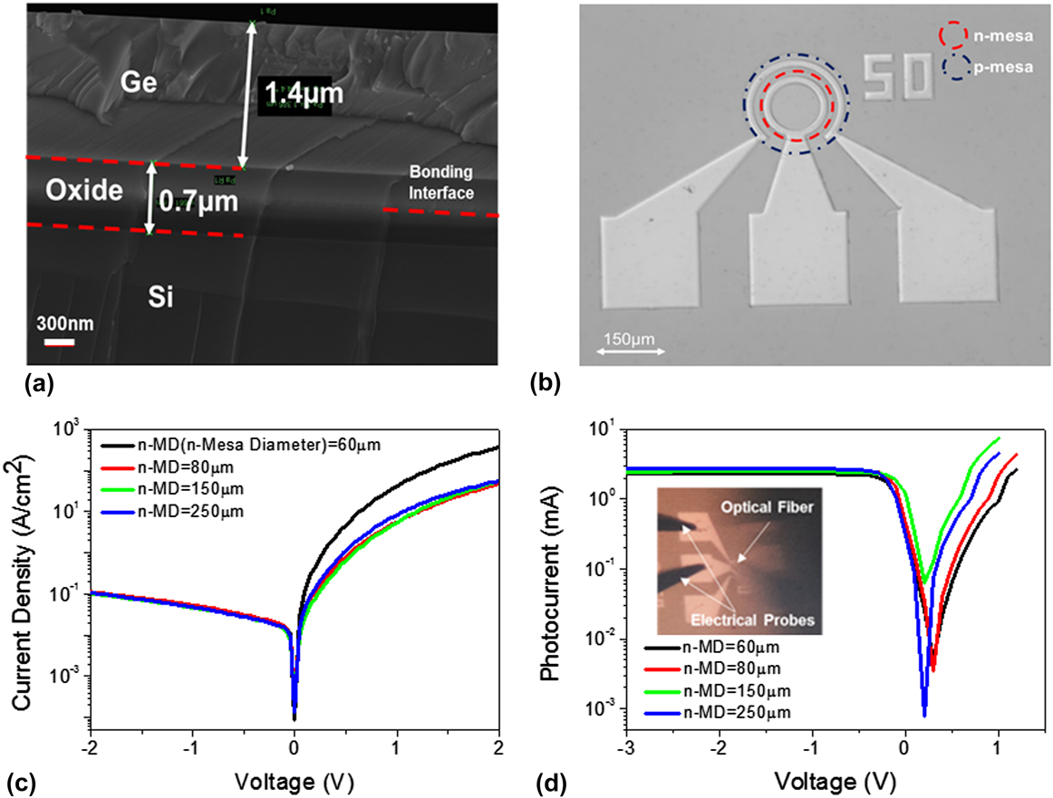
In the authors’ group, vertical p-i-n photodetectors on the GOI platform were developed. The key fabrication steps were: (i) implanting the boron (B) ions on the Ge/Si substrate; (ii) forming the GOI platform through wafer bonding; (iii) CMP away the misfit dislocations; (iv) implanting the arsenic (As) ions on the GOI wafer to realize the p-i-n GOI structure as shown in Fig. 4(a); (v) forming the n- and p-mesas, (vi) depositing the PECVD SiO2 for passivating the peripheral of the PDs; and (vii) forming the p- and n-contacts.
(a) Cross-sectional SEM image of a GOI p-i-n structure. (b) Optical microscope image of the fabricated GOI p-i-n photodetector with n-mesa diameter of 150 µm. (c) Current–voltage characteristics of the GOI p-i-n photodetectors with different n-mesa diameters. (d) Photocurrent of the GOI p-i-n photodetectors with respect to the applied bias. Inset shows the corresponding measurement configuration.
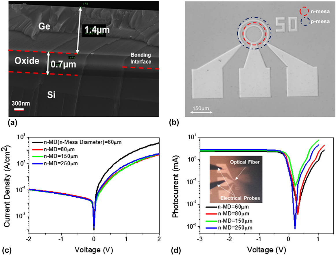
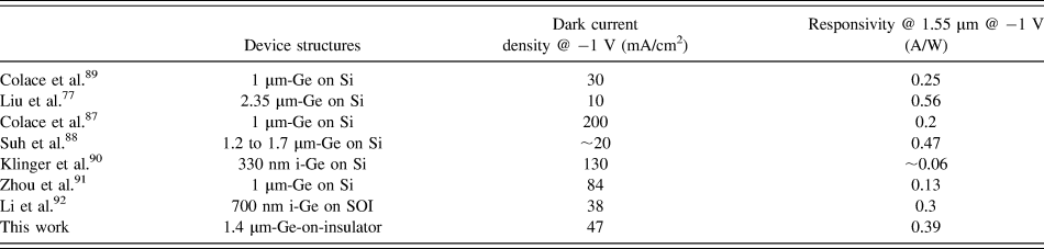
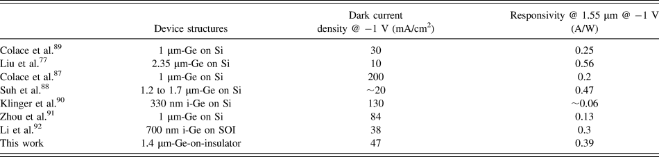
Figure 4(b) shows the optical microscope image of the fabricated GOI p-i-n photodetector with an n-mesa diameter of 150 µm. The image reveals clear device surface features of mesa regions and metal contacts. Figure 4(c) depicts current–voltage characteristics of the photodetectors with different n-mesa diameters. The dark current density of the device is ∼47 mA/cm2 at a reverse bias of −1 V, irrespective of n-mesa diameters. This indicates that there is a negligible surface peripheral leakage current contributing to the device dark current, implying a good quality of SiO2 passivation. The relatively low on/off ratio might be attributed to the high series resistance of metal/Ge contact that hinders the forward-biased current of the photodetector. The series resistance could be further reduced by improving the metal/Ge contact fabrication. Figure 4(d) shows the device photon-generated current with respect to an applied bias voltage under 6.9 mW optical illumination at 1550 nm. The photocurrents saturate at a low reverse bias of −0.4 V, enabling the low-power consumption capability of the devices. The ∼2.6 mA saturated photocurrent gives a ∼0.39 A/W device responsivity. The dark current and optical responsivity of the photodetector are comparable with reported values Reference Jung, Hsieh, Kwong, Liu and Brennan74,Reference Colace, Balbi, Masini, Assanto, Luan and Kimerling87–Reference Li, Xue, Liu, Cheng, Li and Wang92 and are summarized in Table II. Considering surface optical reflection and metal contacts shielding, the responsivity of the photodetector is expected to be even higher, demonstrating an excellent potential of the GOI platform as an enabler for the on-chip electronic–photonic integration.
Summary of reported Ge normal-incidence p-i-n photodetectors as benchmark to our GOI photodetector.
IV. Ge LIGHT SOURCES
Si is an indirect bandgap material and its light emission efficiency is extremely low. Although there are several approaches (including erbium (Er)-doped Si, Si-rich oxide, nanocrystal Si, and many more) to pursue an Si light source, none of them are able to offer sufficient EL efficiency at room temperature. Reference Jalali and Fathpour93
Ge has a pseudo-direct bandgap, where the energy difference between the direct bandgap at the Γ valley and indirect bandgap at the L valley is only 136 meV. The energy difference can be further reduced by an appropriate amount of tensile strains. With the biaxial tensile strain, both direct and indirect bandgaps shrink, but the direct bandgap shrinks faster. Hence, it is possible to transform Ge from an indirect to a direct bandgap with a biaxial strain of about >1.75%. Reference Liu, Sun, Pan, Wang, Kimerling, Koch and Michel94–Reference Reboud, Gassenq, Hartmann, Widiez, Virot, Aubin, Guilloy, Tardif, Fédéli, Pauc, Chelnokov and Calvo97 Theoretically, a uniaxial tensile strain of >4% along 〈100〉 direction is also able to realize a direct bandgap of Ge. Experimentally, 0.2–0.3% of tensile strain can be thermally induced during the cooling from high-temperature Ge growth to room temperature as Ge has a linear coefficient of thermal expansion (CTE) of 5.8 ppm/°C compared to Si which has a CTE of 2.6 ppm/°C. This amount of tensile strain reduces the energy difference between the direct and indirect bandgaps to ∼100 meV. Through heavy n-type doping, the indirect L valley can be occupied by electrons from the n-type doping, and some injected electrons are redistributed to occupy the direct Γ valley upon carrier injection. The electrons in the direct Γ valley then recombine with holes radiatively via efficient direct transitions. Michel et al. in Massachusetts Institute of Technology used this approach and reported the first optically pumped Ge/Si laser operating at room temperature in 2010. The Ge/Si substrate had a biaxial tensile strain of 0.24% and was heavily phosphorous (P) doped ∼1 × 10¹⁹/cm3. Reference Liu, Sun, Kimerling and Michel39 An electrically pumped germanium laser was subsequently reported by the same research group two years later. Reference Camacho-Aguilera, Cai, Patel, Bessette, Romagnoli, Kimerling and Michel40
Nam et al. Reference Nam, Sukhdeo, Kang, Petykiewicz, Lee, Jung, Vučković, Brongersma and Saraswat98 proposed a gradually strained Ge microbridge to enable strong carrier confinement. This structure significantly increases the carrier concentration in the active region, resulting in an enhanced emission. Based on the similar idea, another group has demonstrated an enhanced photoluminescence at a wavelength as long as 5 μm in uniaxial tensile strained GOI (on Si substrate) microbridges based on highly strained Ge cavities. Reference Zabel, Marin, Geiger, Bozon, Tardif, Guilloy, Gassenq, Escalante, Niquet, Duchemin, Rothman, Pauc, Rieutord, Reboud, Calvo, Hartmann, Widiez, Tchelnokov, Faist and Sigg99 In the authors’ group, we have demonstrated a gradually strained Ge microbridge structure with a pair of distributed Bragg reflector (DBR) mirrors on Ge stressing pads to form a resonator for light emission applications. The resonator was fabricated on a GOI substrate, and the strains were manipulated through different Ge microbridge structures.
The GOI substrate was fabricated by epitaxy, bonding, and layer transfer processes. The Ge layer was in situ doped to ∼1 × 10¹⁹/cm3 with phosphorous during the Ge growth on an Si (100) substrate. Then the Ge/Si wafer was bonded to a plasma-treated Si (100) substrate with a thermal oxide layer and an Al2O3 sacrificial layer at room temperature. After removing of the Si substrate from the Ge/Si wafer, the n-type GOI could be realized. Finally, a CMP step was used to thin down the Ge film to the desired thickness.
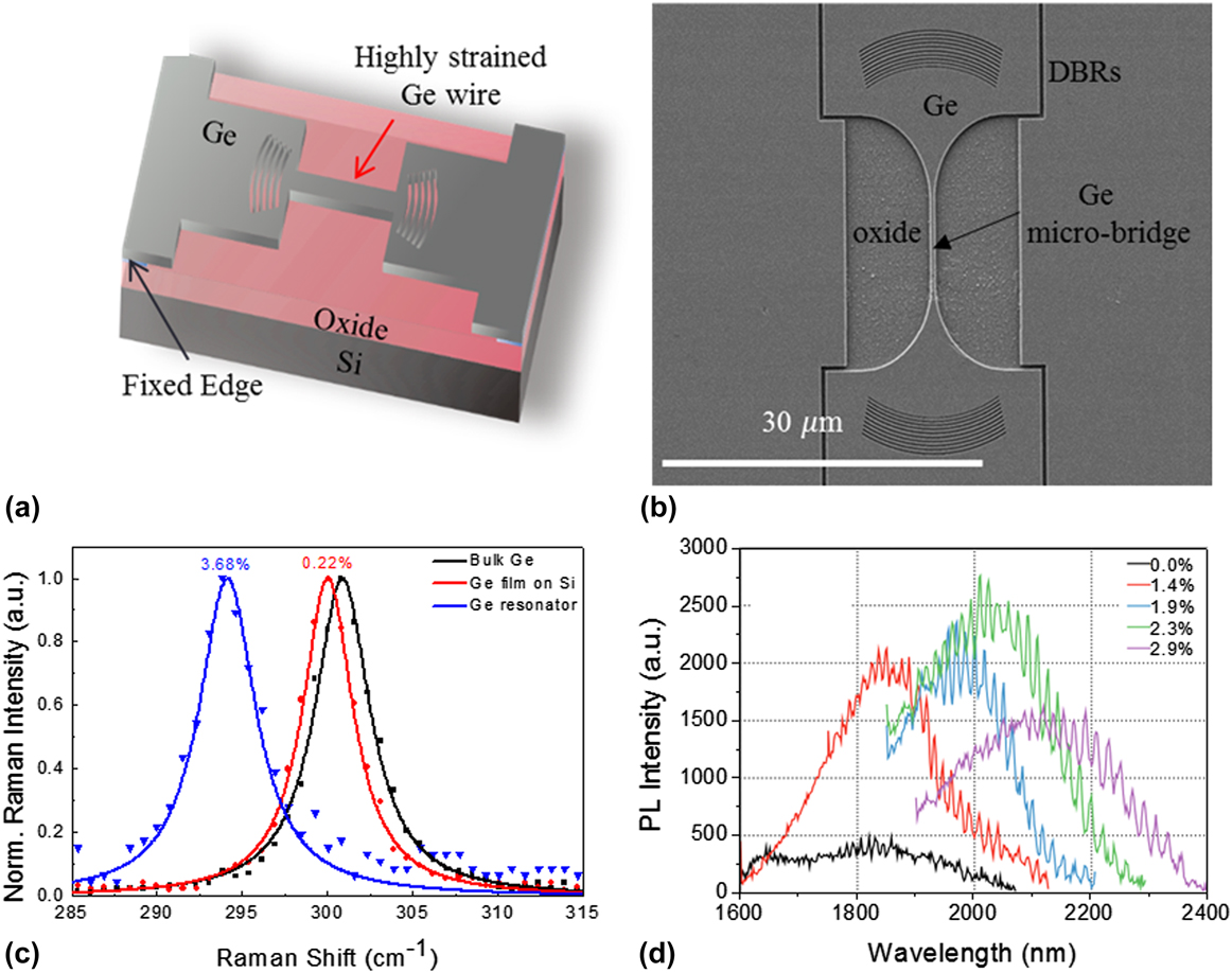
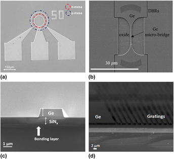
Figures 5(a) and 5(b) represent the schematic and its corresponding scanning electron microscope (SEM) image of the strained Ge micro-bridge resonator. The micro-bridge structure is defined by electron beam lithography, and it is uniaxially tensile strained due to the relaxation of the Ge pads after removal of the sacrificial layer.
(a) Schematic illustration of a strained Ge micro-bridge resonator, and (b) its corresponding SEM image. (c) Raman measurements (scattered points) and Lorenz fitting (solid lines) of a bulk Ge, a Ge/Si substrate and a 3.68% strained Ge resonator. (d) PL spectra of the strained Ge micro-bridge with different strains. It shows that the light emission intensity increases with increasing the tensile strain until reaching the detection cut-off of the detector at 2200 nm.
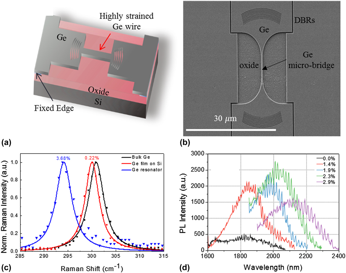
By tuning the length of the Ge pads, the strain on the microbridge can be manipulated. In our structures, the tensile strain varied from full relaxation to 3.68% as measured by the Raman spectroscope, which is based on the nonlinear relation between Raman peak shift and the strain level. Reference Gassenq, Tardif, Guilloy, Duchemin, Pauc, Hartmann, Rouchon, Widiez, Niquet, Milord, Zabel, Sigg, Faist, Chelnokov, Rieutord, Reboud and Calvo100 Figure 5(c) shows that a significant Raman peak shift on a highly strained Ge resonator compared to the Raman peaks from a bulk Ge substrate and a Ge/Si substrate.
The room-temperature PL spectra of the Ge microbridge with different strains are shown in Fig. 5(d). As the tensile strain increases from 0 to 2.3%, it shows a red-shift of the emission peak, while the emission intensity increases. This observation indicates the enhancement of carrier confinement with increasing strain, thus resulting in the increase in the integrated PL intensity of the 2.3% strained resonator by more than 5 times, compared to that of the fully relaxed Ge sample. However, due to the detection limits of the detector, the measured PL intensity decreases as the tensile strain further increases to 2.9%.
By further optimizing the microbridge and DBR structure, the Ge laser can potentially be realised.
V. Ge WAVEGUIDES
Monolithic integration of photonic circuits will not be possible without the successful communication between the various Ge-active components via waveguides. Passive waveguides and active Ge modulators have been fabricated on the GOI platforms. Reference Kang, Takenaka and Takagi101 However, the SiO2 dielectric from the bottom cladding material is highly lossy over 2.5–2.9 µm and above 3.5 µm wavelength. Replacing the SiO2 with sapphire (transparent up to 4.4 µm), SiN (transparent up to 6.6 µm), or air (suspended Ge membrane, transparent up to 6.9 µm) was proposed by Soref et al. Reference Soref, Emelett and Buchwald102
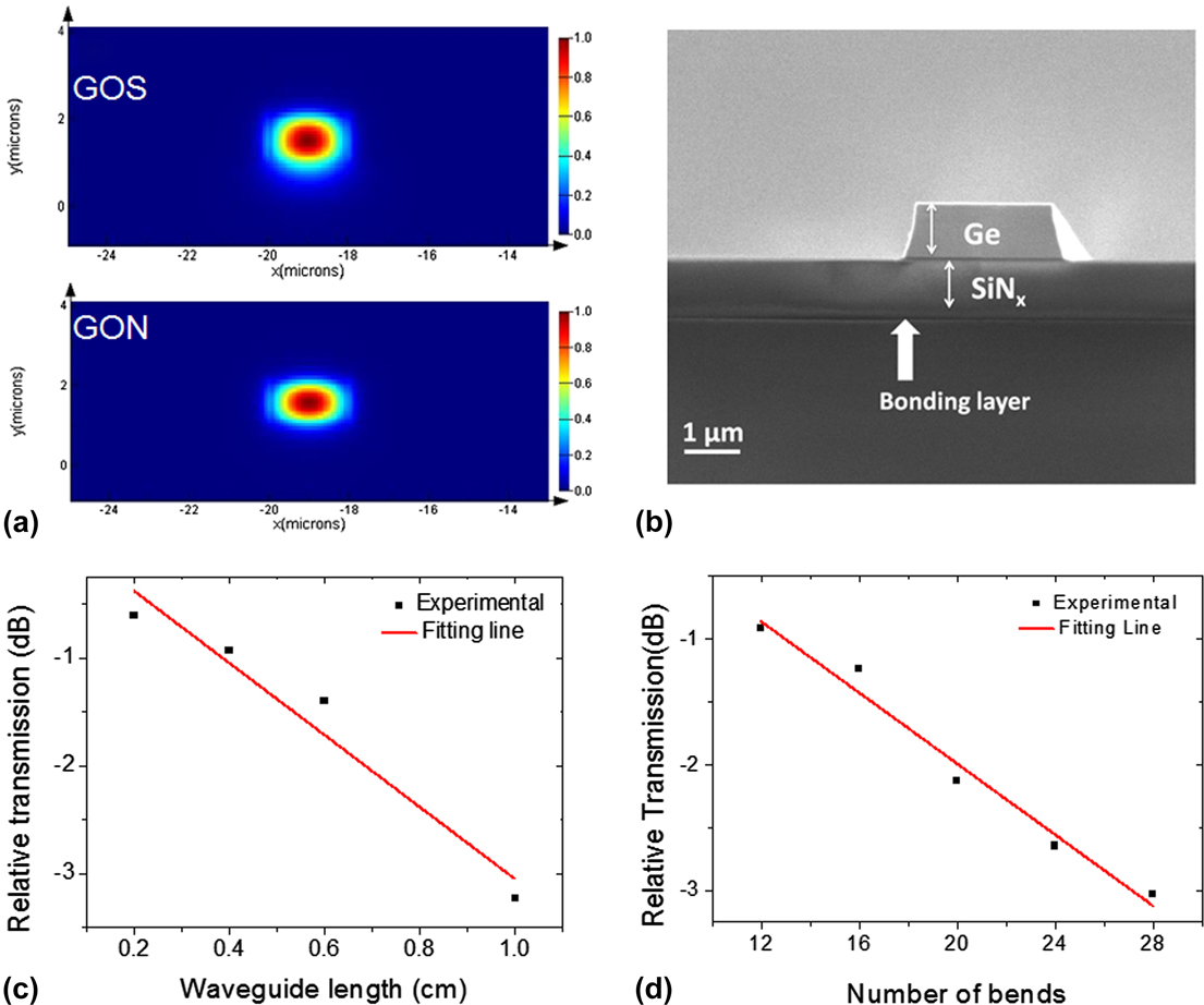
Ge/Si platforms are widely used in photonics research presently, and many impressive achievements have been reported. The lowest propagation loss of Ge waveguides on this platform reported a propagation loss of 0.6 dB/cm. Reference Nedeljkovic, Penadés, Mitchell, Khokhar, Stanković, Bucio, Littlejohns, Gardes and Mashanovich103 However, the refractive index contrast between Ge (n = 4.1) and Si (n = 3.4) is considerably less than that of silicon-on-insulator (SOI, ∆n = 2.01). As a result, the bend radii in Ge/Si must be accordingly larger than those in SOI, causing the footprint of Ge/Si on-chip devices to be generally larger than those of SOI. What is desired is a better alternative Ge-waveguide platform that will provide a larger core-clad index contrast than that of Ge/Si as well as with useful transparency and smaller channel-bend radii. To achieve these goals, the authors’ group has developed the germanium-on-silicon nitride (Ge-on-SiN x ) which is referred to here as GON. The refractive index of silicon nitride (SiN x ) is 1.9 and it is transparent up to about 6.6 µm. In addition, the refractive index contrast of GON is 2.1 compared to 0.7 in Ge/Si and hence a compact ring becomes possible. Moving forward, compact sensing devices Reference Yalcin, Popat, Aldridge, Desai, Hryniewicz, Chbouki, Little, King, Van and Chu104 can also be realized based on microring resonators Reference Xu, Fattal and Beausoleil105 with this innovative Ge platform. Therefore, this GON structure is promising for providing a more compact integrated photonic circuit network whose bend radii are only a few microns. Our simulation result also shows that GON has a better confinement than that of the Ge/Si as shown in Fig. 6(a). The simulation is based on the finite difference time domain method. The thickness of the Ge strip core and the SiN x layer thickness is defined to be 1 µm each, and the operation wavelength is set to 3.8 µm. The cross-sectional dimensions of both waveguides on GON and Ge/Si are determined to support a single TE mode propagation.
(a) Simulation result shows the mode profile of waveguides on a Ge/Si substrate and a GON platform with width = 2 µm and height = 1 µm. (b) Cross-sectional SEM image of the patterned GON wafer. (c) Measurement results of propagation losses of waveguides on the GON substrate. The GON waveguide has a propagation loss of 3.35 dB/cm, while the Ge/Si waveguide has a propagation loss of 8.18 dB/cm (result not shown). (d) Measurement results of the bend losses on the GON waveguide. The bend loss of the GON waveguide is 0.1411 dB/bend and the bend loss of Ge/Si waveguide is 2.54 dB/bend (result not shown).
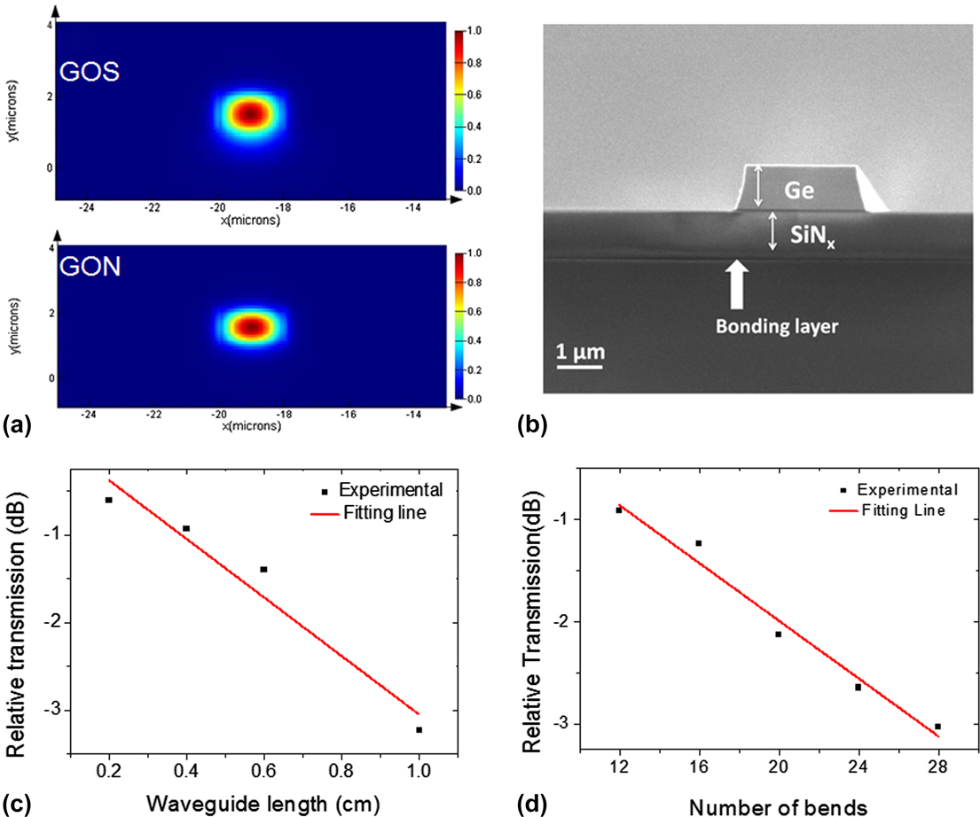
The GON platform can be realized through direct wafer bonding process. Briefly, low stress PECVD SiN x and PECVD SiO2 films were deposited on the Ge/Si substrate. The wafer was then bonded to an Si handle wafer to realize the GON platform. Waveguides on the GON platform with a width of ∼2 µm and a height of ∼1 µm was then fabricated using reactive ion etching (RIE) process as shown in Fig. 6(b). The propagation loss and bend loss measurements were carried out employing the cut-back method. Reference Vlasov and McNab106 This method is based on a comparison of transmissions through waveguides of different lengths or number of bends and fitting the dependence on the length or number of bends assuming identical coupling conditions and an identical surface roughness.
We have fabricated waveguides whose length changes from 2 to 12 mm with a step of 2 mm. Each waveguide has 8 bends (R = 50 µm) and we assume that the total bend losses in 8 bends at this large radius is negligible. The propagation loss measurement results are shown in Fig. 6(c). The GON waveguide has a propagation loss of 3.35 dB/cm compared to 8.18 dB/cm in the Ge/Si waveguide. In addition, the bend loss of the GON waveguide is 0.1411 dB/bend, which is also lower than the Ge/Si waveguide of 2.54 dB/bend as shown in Fig. 6(d). The higher propagation and bend loss of the Ge/Si waveguide are because the mode interacted intensively with the interface and sidewall due to the poor confinement. We believed the propagation loss of the GON waveguide can be further reduced with finer lithography and deep-reactive ion etching (DRIE). For certain applications, we can design rib structures to realize a better mode confinement thus reducing the propagation loss. Reference Suh, Kim, Joo and Kim88 The largest source of bend loss is from the mode mismatch loss. It is due to the imperfect mode overlap between the straight and the bent waveguides. This leads to scattering at the start and at the end of fixed-radius bends. We expect to further reduce the bend loss of the GON waveguide by varying the curvature of the bend continuously rather than abruptly. Reference Li, Yao, Thacker, Mekis, Zheng, Shubin, Luo, Lee, Raj and Cunningham107
This GON platform has the potential of making passive photonic devices with footprints as small as possible, which can be useful for compact active devices like microring modulators.
VI. Ge WAVEGUIDE FOR SENSOR APPLICATIONS
The Ge/Si platforms are also gaining a wide interest for sensing in the mid infrared (MIR) regime due to its broad optical transparency ranging from 2 to 9 μm. Reference Soref108 The MIR spectral region is analytically relevant, as an extensive range of liquid and gas phase molecules interact with MIR photons with the excitation of their rotational and vibrational modes. Reference Lavchiev and Jakoby109 Thus, it is appropriate to develop a lab-on-chip sensing platform using Ge thin films in the MIR region. Several studies report label-free chemical and biological sensing and diagnostics, environmental monitoring, and the development of hand-held devices using Ge thin film waveguides. Reference Sieger and Mizaikoff110
Given the large compatibility of Ge substrates to silicon processing methods, on-chip integration to develop point of care devices can be realized with ease. Reference Sieger, Balluff, Wang, Kim, Leidner, Gauglitz and Mizaikoff111 One of the recent studies involves the detection of cocaine using low loss Ge ridge waveguides. Reference Chang, Wägli, Paeder, Homsy, Hvozdara, van der Wal, Di Francesco, de Rooij and Peter Herzig112 A MIR radiation source at a wavelength of 5.8 μm was coupled into the waveguide. The analyte (cocaine dissolved in tetrachloroethylene) was allowed to interact with the evanescent field by utilizing a microfluidic chamber, built and bonded over the Si substrate with the Ge waveguide. With the modulation of cocaine concentration in the solution, a minimal concentration of 100 μg/L was detected. However, the issue of large propagation losses observed on the Ge structures presents a limitation for developing highly sensitive on-chip platforms. The process of polishing the coupling facets (in and out for butt coupled designs) to improve surface quality is quite tedious and could lead to higher scattering losses. In the authors’ group, we have demonstrated the sensing capability of a grating-coupled Ge/Si waveguide (with reduce the losses) in the MIR region using isopropyl alcohol (IPA) as an analyte.
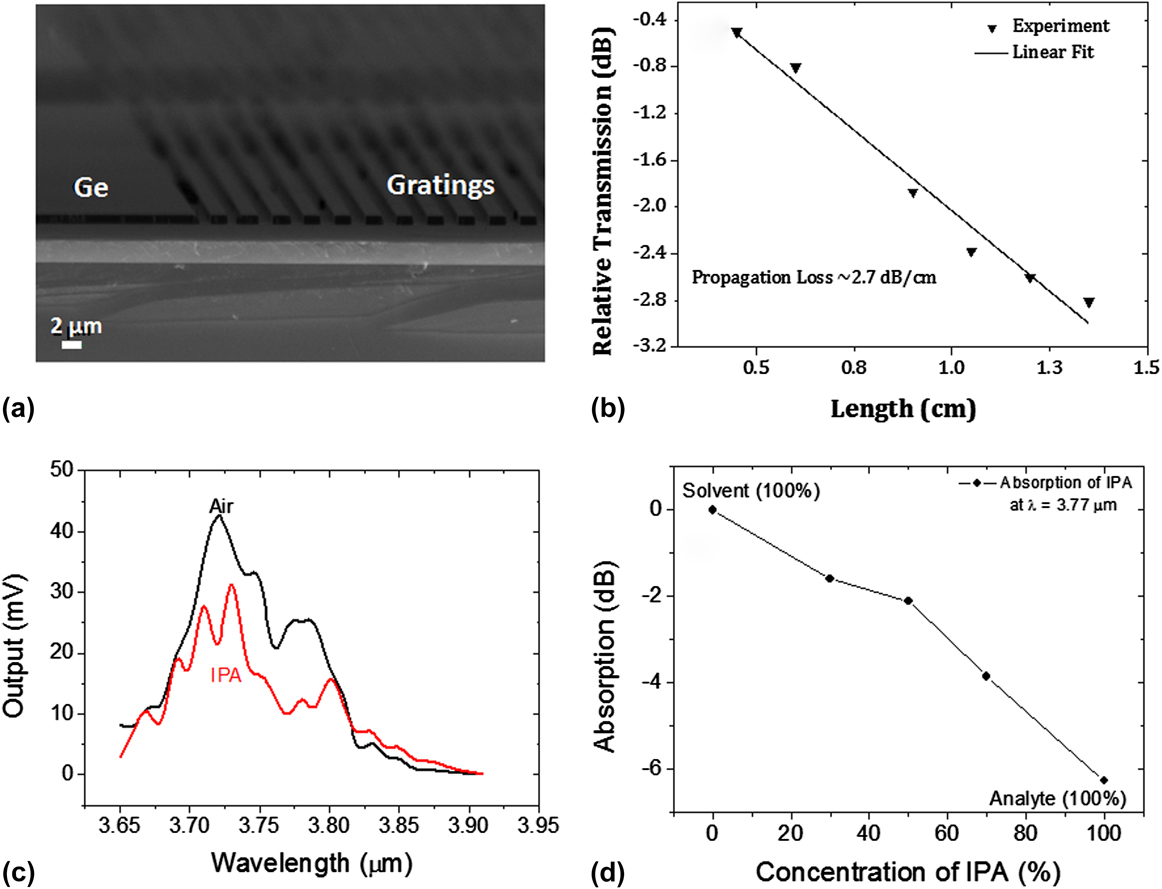
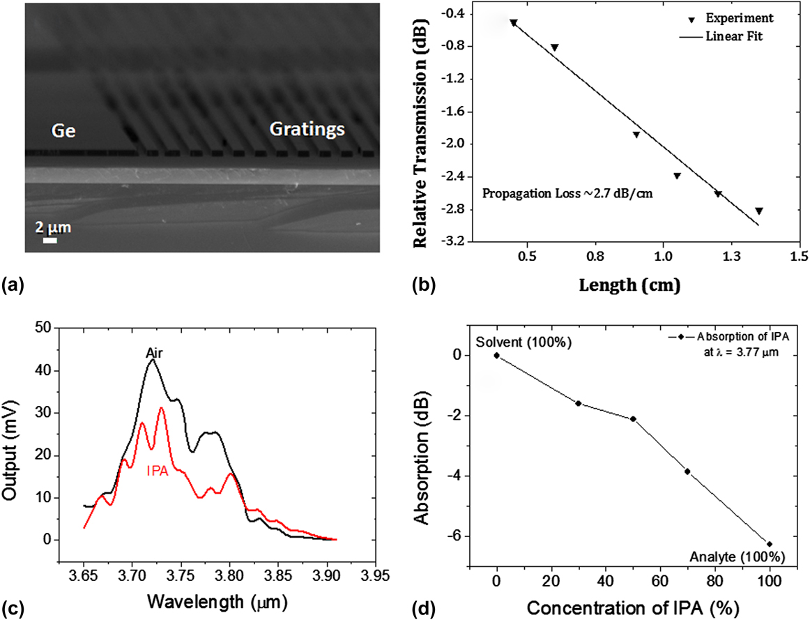
Ge/Si waveguides were fabricated on a 3 µm thick Ge layer that was grown directly on a silicon wafer. Electron beam lithography was used to pattern the grating structure on the Ge/Si wafer and the grating pattern was then transferred to Ge layer through deep-reactive ion etching (DRIE). Rib waveguides with a depth of 1.5 µm and with a single mode propagation were obtained with a grating duty cycle of 0.5. Single mode waveguides with a width of 2 μm and a length of 1.5 μm were fabricated to enable sensing over a larger region. Rib waveguides are optimum for having a large evanescent field and are thus compatible to be used for sensing applications. The fabricated samples were characterized for propagation loss using the cut-back method, with a fiber coupled angle maintained at 10°. The measured wavelength was fixed at 3.77 µm. Figure 7(a) shows the SEM image of the Ge-on-Si waveguide and grating structures which are etched using the DRIE method. The relative transmission is measured with respect to the increasing waveguide length. A low propagation loss of 2.7 dB/cm is obtained and is shown in Fig. 7(b). The well-defined waveguide structures minimize the scattering loss and thus a low propagation loss is observed.
(a) SEM image of Ge/Si waveguides and grating structures. (b) Propagation loss of the waveguides measured by cut-back method. (c) Light absorption of an organic solvent IPA in the MIR region, obtained by droplet casting onto the Ge/Si waveguide. (d) Change in absorption observed with increase in IPA (analyte) concentration. Water is used as a solvent in this case. A good linearity in sensor responsivity is observed.
For analytical applications, the evanescent field generated from the photonic device in use is beneficial. As for the rib waveguide structure, the evanescent field is generated at the interface of the waveguide (high refractive index) and the surrounding medium (low refractive index). When the analyte molecules are allowed to interact with this evanescent field, the light absorption by these molecules leads to an attenuation of the wave propagating within the waveguide. Thus a reduced output intensity would be evident. This occurs in correspondence to the molecules’ vibrations and/or rotations. The absorption (A) within the evanescent field thus follows Reference Hu, Tarasov, Agarwal, Kimerling, Carlie, Petit and Richardson113 :
 $$A = \left( {\varepsilon cl} \right)r = \log \left( {{{{I_{{\rm{ref}}}}} \over I}} \right)\quad ,$$
where ε is the molar absorptivity, l is the waveguide length, c the concentration, and r is the radiative energy within the evanescent field. I ref and I are the intensity of the output power of the nonabsorbing media and absorbing media, respectively. Two types of interactions between the waveguide and the liquid analyte can be implemented. The first experimental study involves a droplet casting method to obtain the absorption spectra of the analyte. Secondly, a microfluidic channel could be built around the waveguide to contain the analyte for a more efficient and repeatable testing approach.
In this study to evaluate the label-free sensing capability of the Ge/Si waveguide in the MIR region, IPA was chosen as the primary analyte with water as the solvent in the preliminary studies. An optical scan using a tunable quantum cascade laser (QCL) light source was carried out (wavelength range of 3.65–3.9 µm) through the 1.5 cm long Ge/Si waveguide. A first scan was carried out without the incorporation of the analyte onto the waveguide surface. The surrounding medium was exposed to the air. Subsequently, a 0.1 mL liquid droplet of IPA was casted on the center of the Ge waveguide and the corresponding light intensity was recorded. The output values from the optical scan obtained for the two varying adjacent mediums are shown in Fig. 7(c). The main absorptions are attributed to the characteristic absorption band of the hydroxyl group (–OH) and the C–H stretching modes of the methyl group (–CH3) comprising of the IPA molecules. Reference Coates114 These modes have been identified to have a wide influence on the absorption spectra in the MIR region. From Fig. 7(c), it is observed that the maximum absorption occurs at 3.77 µm. Furthermore, the influence of the change in concentration of the analyte on light propagation is observed. A wavelength of 3.77 µm is fixed at the highest absorption by the IPA molecules. The concentration of IPA is varied from 0 to 100%, and water is utilized as the solvent for this characterization. Water molecules have been observed to have no absorption at this given wavelength of 3.77 µm. The increase in absorption is calculated according to Eq. (5) and is shown in Fig. 7(d) with an increase in the IPA concentration. As the volume concentration of the analyte increases, a good linearity in the sensor response is demonstrated. Thus, the sensing capabilities of the Ge-on-Si waveguide is clearly demonstrated with the use of IPA as the analyte.
To further improve the sensitivity, a smaller waveguide loss (dependant on the waveguide design and material) and a larger evanescent field is preferred as it can enhance the output signal from the sensor device. Through integrating the microfluidic channels onto the waveguide chip, cost effective and mass producible lab-on-chip sensing platforms can be realized. Furthermore, introducing intermediate dielectric materials can result in a large refractive index contrast. This enables more compact devices, higher sensitivity with improved limits of detection, and sensing of a variety of analytes. Depending on the dielectric materials, the applicable wavelength can also be extended. Thus some of the work involving the development and testing of the GON Reference Li, Anantha, Bao, Lee, Guo, Hu, Zhang, Wang, Soref and Tan115 waveguide structure for sensing applications using microfluidic channel integration is in-progress.
VII. FUTURE WORK—Sn INCORPORATION
As the absorption coefficient of Ge drops drastically beyond its direct bandgap (0.8 eV, equivalent to 1550 nm), it cannot cover the L-band (1565–1625 nm) and the U-band (1625–1675 nm) of telecommunication wavelengths. Although introducing an in-plane tensile strain can extend the Ge absorption edge through high-temperature annealing or through depositing Si3N4 stress liner, Reference Capellini, Kozlowski, Yamamoto, Lisker, Wenger, Niu, Zaumseil, Tillack, Ghrib, Kersauson, Kurdi, Boucaud and Schroeder116,Reference Ghrib, Kurdi, Prost, Sauvage, Checoury, Beaudoin, Chaigneau, Ossikovski, Sagnes and Boucaud117 it still fails to cover the entire L-band. Tin (Sn), is another group IV semiconductor, has a narrower direct bandgap than that of Ge and can reduce the bandgap energy of Ge through incorporation of Sn into Ge during the Ge growth. Ge1−x Sn x becomes a direct bandgap material when the Sn incorporation is 8–10 at.%. Reference D’Costa, Cook, Birdwell, Littler, Canonico, Zollner, Kouvetakis and Menéndez118–Reference Wirths, Buca and Mantl121 Grutzmacher et al. demonstrated an optically pumped Ge0.874Sn0.126 laser on the Si substrate at low temperature. Reference Wirths, Geiger, Driesch, Mussler, Stoica, Mantl, Ikonic, Luysberg, Chiussi, Hartmann, Sigg, Faist, Buca and Grutzmacher122 Separately, a Ge0.97Sn0.03/Si p-i-n photodetector also demonstrated its reasonable responsivities from 1310 to 1800 nm. Reference Su, Cheng, Xue, Wang, Cao, Xue, Hu, Zhang, Zuo and Wang123 Hence, GeSn is a promising material for future Si photonics components.
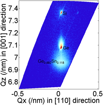
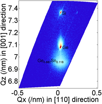
GeSn alloy growth on an Si substrate is a challenging process due to the following reasons: (i) the equilibrium solid solubility between Ge and Sn is very low, <1%; (ii) lattice mismatch between Ge and α-Sn is large, about 14.7% (a Ge = 5.658 Å and a α-Sn = 6.489 Å); and (iii) significant surface segregation of Sn at elevated temperatures, >400 °C. Despite these limitations, our group has overcame these challenges and successfully grown GeSn on Si substrates through a Ge buffer layer. Sn with a concentration as high as 11.8% and with a thickness of 150 nm has been grown on the Ge/Si substrate as shown in Fig. 8. More photonic devices, such as lasers, photodetectors, and waveguides based on the GeSn/Ge/Si substrate are being attempted and developed.
Symmetric (004) reciprocal space map of a GeSn/Ge/Si structure measured from high resolution X-ray diffraction. The Sn composition is ∼11.8%.
VIII. APPLICATION OF INTEGRATED ELECTRONIC–PHOTONIC CIRCUITS
With the development of the photonic devices as shown above, a fully integrated light detection and ranging (LiDAR) chip using GOI on a silicon platform is one of the many possible applications. The Ge light source, together with other components such as waveguides, photodetectors, and gratings can be realized on the GOI platform. Additionally, the electronic components such as CMOS for high-speed data processing can be built on the Si substrate enabling future optoelectronic integrated circuits (OEIC). Hence, a fully monolithic integrated electronic-photonic such as a LiDAR chip can be realized. The LiDAR chip can even be mass produced by Si foundries due to the material’s compatibility with Si.
A compact and portable hand-held sensor is another application that we are interested in. Since most organic fluids are sensitive in MIR regions, the sensor based on the Ge/Si platform becomes a very promising candidate. Similar to the above approach, a sensor comprises of a Ge light source, waveguides, and CMOS (for data processing) can be monolithically integrated on the GOI on the Si platform. The form factor of the sensor can be greatly reduced since most of the optic components can be omitted or miniaturized. Hence, it is possible that this sensor chip can be built-in with wearable or portable electronics, such as smart watch, smart phone, etc.
IX. CONCLUSIONS
In summary, we have demonstrated two approaches to achieve highly crystalline germanium-on-silicon substrates. The first approach is based on high-temperature annealing of a GOI substrate in oxygen ambient and threading dislocation densities of low-106/cm2 can be achieved. The next approach is to dope the germanium seed layer with arsenic, and threading dislocation densities of mid-106/cm2 can be realized. Devices such as photodetectors, lasers, waveguides, and sensors are then co-fabricated on these substrates and they demonstrate promising performances to realize a true OEIC. The incorporation of tin into germanium reveals the next generation of Si photonics platform with better performance and multiple functionalities. With all these efforts, we believe that a fully silicon-based integratable and manufacturable LiDAR chip and a hand-held portable sensor become viable.
ACKNOWLEDGMENTS
This research was supported by the National Research Foundation Singapore through the Singapore MIT Alliance for Research and Technology’s Low Energy Electronic Systems (LEES) IRG and NRF-CRP12-2013-04. The work was also partially supported by Innovation Grant from SMART Innovation Center. Authors are grateful to the support and resources from the Silicon Technologies Center of Excellence (Si-COE). C.S. Tan is affiliated with NOVITAS (Nanoelectronics Center of Excellence) at NTU. S. Bao is supported by SMA3 Fellowship. We would like to thank Daeik Kim, Chibuzo Onwuka and Donguk Nam from Inha University for their measurement data and valuable discussion. In addition, we are thankful for the support received from the silicon photonics group, Optoelectronics Research Center at the University of Southampton.