I. INTRODUCTION
Since the discovery of the first graphene flake in 2004 through the mechanical cleavage of highly ordered pyrolytic graphite, two-dimensional (2D) nanomaterials have attracted attention due to their potential use in a range of applications such as catalysis, electronic and optoelectronic devices, electrodes for energy storages, and nanocomposites.Reference Novoselov, Geim, Morozov, Jiang, Zhang, Dubonos, Grigorieva and Firsov1,Reference Novoselov, Jiang, Schedin, Booth, Khotkevich, Morozov and Geim2 2D materials such as graphene have versatile and enhanced mechanical, chemical, and electrical properties.Reference Pan, Bao, Mao, Liu and Li3,Reference Sun, Liu, Yin, Yu, Li, Hang, Zhou, Yu, Li, Tai and Guo4 The success of 2D graphene has motivated scientists in the last years to pursue the search for 3D materials that can be exfoliated by separating a 3D material into single or few 2D layers.Reference Mounet, Gibertini, Schwaller, Campi, Merkys, Marrazzo, Sohier, Castelli, Cepellotti, Pizzi and Marzari5 These efforts successfully have led to the discovery of promising new 2D materials beyond graphene such as hexagonal boron nitride and transition metal dichalcogenides.Reference Marrazzo, Gibertini, Campi, Mounet and Marzari6,Reference Pacilé, Meyer, Girit and Zettl7 Therefore, the space of 2D materials is expanding and getting more mature as a distinct class of materials bringing new capabilities, functionalities, and technologies, which were not attainable with their parent 3D materials.
Layered metal oxides, nitrides, and carbides are already being explored and were found to be promising 2D materials for different electronic devices.Reference Gupta, Sakthivel and Seal8 To date, there is no literature about 2D materials based on metal borides, while there are many advantages of pursuing metal borides as 2D materials such as low temperature synthesis, especially aluminum. In addition, AlB2 has the unique properties of boron, and more cost-effective and practical to produce than pure boron, which is similar to graphene oxide, as compared to graphene.Reference Thakur and Karak9 Furthermore, AlB2 single crystals show metallic conductivity in the axis parallel to the basal hexagonal plane.Reference Burkhardt, Gurin, Haarmann, Borrmann, Schnelle, Yaresko and Grin10 In terms of potential applications, AlB2 flakes were found to be a very effective reinforcement for polymer composites such as epoxies, with outstanding mechanical performance.Reference Savaş and Kayikci11,Reference Deppisch, Liu, Hall, Xu, Zangvil, Shang and Economy12 Therefore, AlB2 flakes can be utilized for conductive polymer composites. Due to the hexagonal structure, thermal and chemical stability, and electrical conductivity, metal borides have been used as substrates for heteroepitaxial growth of semiconductor devices.Reference Suda and Matsunami13,Reference Yamada-Takamura, Wang, Fujikawa, Sakurai, Xue, Tolle, Liu, Chizmeshya, Kouvetakis and Tsong14
The hexagonal crystal structure of AlB2 is one of the simplest inorganic structure types: a simple hexagonal cell of aluminum atoms with two boron atoms occupying the trigonal prismatic sites. The boron atoms form graphite-like sheets with the layers arranged into honeycomb-like structures separated by a lattice parameter (c) of 3.25 Å. AlB2 is a MB2 type material where M is for metals, and it has a metastable phase at room temperature.Reference Hoffmann and Pöttgen15,Reference Loa, Kunc, Syassen and Bouvier16
Two morphologies of AlB2 crystallites have previously been identified—a low aspect ratio (LAR) equiaxed form of micron length, commonly used in grain refining of aluminum alloys, and a high aspect ratio (HAR) flake of up to a centimeter in width.Reference Matkovich, Economy and Giese17–Reference Serebryanskii and Epel’baum20 The growth of HAR AlB2 single crystal flakes within an aluminum melt was demonstrated starting with a master alloy containing LAR AlB2, which was heated above the Al–B liquidus region followed by various heat treatments.Reference Deppisch, Liu, Hall, Xu, Zangvil, Shang and Economy12,Reference Deppisch, Liu, Shang and Economy21 The study by Hall and Economy showed that HAR flakes could be synthesized by heating merely above the Al(L) + AlB12 ↔ AlB2 peritectic transition temperature, which is permitted by the lengthy growth time of AlB12 from the Al–B melt.Reference Hall and Economy22 In addition, aluminothermic processes have also been used to synthesize HAR AlB2 flakes.Reference Hall and Economy23
There are significant advantages of achieving a smoother substrate with less surface features/defects in order to grow high quality epitaxial thin films. First, a uniform growth of thin films demands substrates that have both smooth and flat surfaces at the atomic level to avoid inhomogeneous nucleation and growth of the film. A rough surface can result in film growth with islands especially as the thickness of the deposited film is reduced. Moreover, the surface roughness is a key factor for the oxidation kinetics since oxidation proceeds in a layer-by-layer manner. Therefore, reducing surface heights and defects will reduce the thickness of the surface oxide layer achieving a thin complete oxide layer. Typically, polishing processes such as chemical–mechanical polishing are used to smoothen the surface roughness of the substrate. This was successfully achieved herein using the mechanical cleavage of the substrate without the need for any extra polishing or etching of the substrate’s surface, which simplified the synthesis process of the TiO2 film. Once this atomically flat surface is achieved using cleavage, its stability against oxidation and surface reconstruction over short time in air is another critical requirement.Reference Padova, Ottaviani, Quaresima, Olivieri, Imperatori, Salomon, Angot, Quagliano, Romano, Vona, Muniz-Miranda, Generosi, Paci and Lay24 Rapid oxidation after cleavage can result in the roughening of surface.Reference Ohsawa, Hayashi, Hasunuma and Yamabe25 Therefore, a low oxidation degree of the substrate is favorable for epitaxial thin film growth.
In this work, we show that millimeter-scale HAR AlB2 crystals grown in situ in an aluminum melt are cleavable via dry mechanical exfoliation resulting in 2D AlB2.Reference Kim, Kim and Huang26–Reference Li, Lu, Wang, Yin, Cong, He, Wang, Ding, Yu and Zhang28 This is of interest to investigations toward low-dimensional boron phases,Reference Mannix, Zhou, Kiraly, Wood, Alducin, Myers, Liu, Fisher, Santiago, Guest, Yacaman, Ponce, Oganov, Hersam and Guisinger29–Reference Feng, Zhang, Zhong, Li, Li, Li, Cheng, Meng, Chen and Wu31 as a surface for epitaxial growth experiments, and the relatively high p-type conductivity (7.5 μΩ cm) of the AlB2 phase in the basal plane.Reference Loa, Kunc, Syassen and Bouvier16 We monitored the surface of cleaved AlB2 in terms of roughness and oxidation using atomic force microscopy (AFM) and secondary ion mass spectrometry (SIMS), respectively. The 2D cleaved flakes were found to be stable under ambient conditions for sufficient time to carry out the subsequent thin film growth of TiO2 using atomic layer deposition (ALD).
II. EXPERIMENTAL DETAILS
A. Fabrication of HAR flakes
Initially, an aluminum–boron (5 wt%) master alloy (KB Alloys, Wayne Pennsylvania) was alloyed with a 99.99% pure aluminum ingot (Alcoa, Pittsburgh, Pennsylvania) by heating to 750 °C in an alumina crucible under flowing argon atmosphere and then cast in a cylindrical graphite mold. To produce the HAR flakes in an aluminum solution, a cast ingot was then heated to 1360 °C (above liquidus temperature) under flowing argon in an alumina crucible and then cooled to 900 °C (below peritectic temperature) for one hour after which the sample was allowed to cool to room temperature at a rate of 0.2 °C/min. HAR AlB2 flakes were then extracted by etching away the aluminum matrix by 37% hydrochloric acid (Fisher Scientific, Waltham, Massachusetts), which yielded aluminum chloride (AlCl3) precipitates and hydrogen gas. HAR AlB2 flakes were separated from the liquid phase by vacuum filtration using a Büchner funnel (Sigma Aldrich, St. Louis, Missouri). Wet residue, composed of aluminum chloride powder and HAR AlB2 flakes, was then washed with copious deionized water followed by isopropanol and dried in a convection oven at 110 °C. The as-grown flakes were then separated from the powder by gentle sieving by hand with a 90 μm mesh sieve. This was followed by gentle flush with isopropanol and subsequent drying at 110 °C for 2 h. The as-grown flakes did not form an oxide layer during synthesis because they were protected from oxygen by the argon atmosphere, and more importantly by the aluminum melt. The native oxide formed during and after the extraction and drying process from exposure to atmospheric oxygen rather than the free oxygen in the aluminum melt.
B. AFM
The AFM images were scanned using a Cypher AFM instrument (Asylum Research, Santa Barbara, California). The scans were carried out in the noncontact mode and with an 8 nm diameter silicon tip, and a scan rate of 0.5 Hz and 512 samples per line.
C. Nanoindentation
The mechanical properties were measured using a commercial indenter, TI Premier (Bruker, Minneapolis, Minnesota), and the experiments were carried out using load-control mode. A cube corner probe was used (tip radius of 40 nm) to maintain shallow indentation depths. For all experiments, 5 s time periods for loading and unloading and 2 s dwell time at maximum nanoindentation load were used. The hardness (H) and reduced elastic modulus (E r) were obtained from the first one-third of the unloading curve according to the Oliver and Pharr method.Reference Mannix, Zhou, Kiraly, Wood, Alducin, Myers, Liu, Fisher, Santiago, Guest, Yacaman, Ponce, Oganov, Hersam and Guisinger29 The indenter probe was calibrated using a standard fused quartz sample.
D. X-ray diffraction
A Siemens/Bruker (Madison, Wisconsin) D-5000 X-ray diffraction (XRD) system (Radiation is Cu Kα and wavelength is 0.15418 nm) is used to obtain crystallographic structure determination.
E. SIMS
A CAMECA 4f SIMS (Madison, Wisconsin) was used in the dynamic mode, for the measurement of the thickness of the oxide layers. The profiling was done with 14.5 keV Cs+ ion beam (raster 500 × 500 µm2, image collimation diameter 50 µm, and sputtering rate 0.01 nm/s).
F. ALD
An Ultratech/Cambridge NanoTech, Savannah S200 ALD system (Waltham, Massachusetts) is used to deposit TiO2. ALD allows atomic-level control for the growth, which results in an epitaxial growth of the film.
III. RESULTS AND DISCUSSION
A. Nanomechanical properties
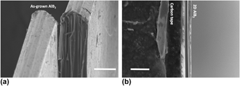
The as-grown flakes were secured on AFM metal disks using an adhesive and left to dry overnight in a well-ventilated room. Mechanical cleavage was then performed using mechanical exfoliation (3 M scotch tape) inside a glove box filled with argon gas. The scotch tape was pressed on the flake and gently peeled up. This exposed the ultra-smooth pristine interior with an extremely flat surface. Figures 1(a) and 1(b) show SEM cross-sectional views of both the as-grown and cleaved flakes. The thicknesses were 6 and 10 µm for cleaved and as-grown flakes, respectively. The mechanical cleavage removed about 4 µm thick layer of the as-grown flake and was facilitated by the Kirkendall void formed due to diffusion rate differences and compositional gradients encountered during the synthesis of AlB2 flakes. The cross-sectional SEM image in Fig. 1(a) shows the length scale and orientation of these voids pointing to morphological origins of the flake formation above the liquidus temperature. Similar Kirkendall voids were observed with other binary alloy systems of Al, specifically Ti–Al and Ni–Al systems.Reference Paul, van Dal, Kodentsov and van Loo32 However, to the best of our knowledge, this is the first scientific study reporting the presence of planar Kirkendall voids in AlB2 flakes.
Cross-sectional SEM images for the (a) as-grown and (b) cleaved AlB2 surfaces. Scale bar is 10 µm.

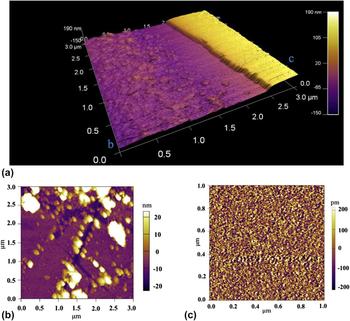
Figure 2(a) shows a step between the surfaces of the as-grown and cleaved flakes. Figure 2(c) shows the cleaved surface over a large area (10,000 × 10,000 Å) with an R q roughness of 1.07 Å and a z-height noise floor of 0.5 Å. The unit cell, c o, is found to be 3.01 Å. The cleaved flake has 80 times lower R q roughness than the as-grown flake, which has significant defects and intermetallic formations [see Fig. 2(b)].
(a) AFM of the AlB2 flake showing a step generated after cleavage, (b) as-grown, and (c) cleaved surfaces.

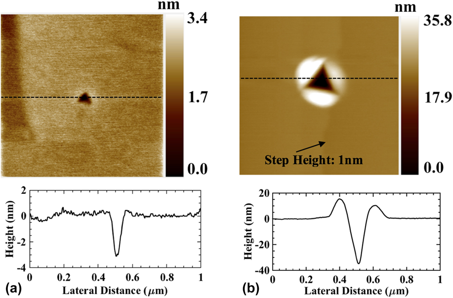
The nanoindentation probe was calibrated according to the Oliver–Pharr method between contact depths of 3–65 nm.Reference Oliver and Pharr33 Figure 3(a) shows the residual image of a 150 µN peak load indentation, measured on the cleaved surface. The cross-sectional profile shows atomic-scale topography in Fig. 3(a), where 3 Å height accounts for an atomic step height. There is no clear pile-up under this indentation load. For a higher indentation load of 720 µN, Fig. 3(b) illustrates a significant pile-up around the indentation mark. The pile-up phenomenon shows highly crystallographic localized material flow.Reference Wang, Raabe, Klüber and Roters34
Residual indentation images and cross-section profiles (1 × 1 µm) after (a) 150 µN and (b) 720 µN indentation load on the cleaved sample under ambient dry conditions.

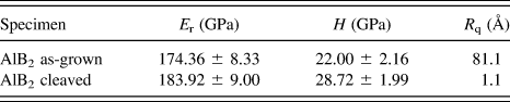
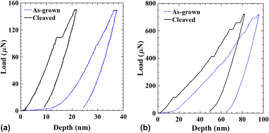
Table I provides the extracted nanomechanical properties of both samples: as-grown AlB2 and cleaved AlB2 flakes. The cleaved sample had higher elastic modulus and hardness. The reduced elastic modulus value (∼174 GPa) was close to the bulk modulus measurement available both as a simulated/calculated value provided by Duan et al.,Reference Duan, Sun, Guo, Peng, Zhu and He35 Shein and Ivanovskii,Reference Shein and Ivanovskii36 and Gaillac et al.Reference Gaillac, Pullumbi and Coudert37 Figures 4(a) and 4(b) show representative load/displacement curves for both samples for indentation loads of 150 and 720 µN, respectively. There were discrete fracture events in both samples, being more pronounced in the cleaved sample. The first fracture event in the cleaved sample took place in depths of 3–5 nm where the tip broke through a specific number of layers, where c = 3.25 Å. Therefore, for such nanoindentation depths, it was about 10–15 layers. These pop-in events in the loading part of the load–displacement curve of the cleaved sample were attributed to transverse cracking due to relatively lower incompressibility of AlB2 on the plane of hexagonal symmetry.Reference Deppisch, Liu, Shang and Economy21 This response is further amplified by the high Zener anisotropy as shown through first-principles calculations.Reference Duan, Sun, Guo, Peng, Zhu and He35 Through the introduction of the freshly cleaved surface, we eliminated the inherent structural compliance of the flake originating from the Kirkendall void, which clearly manifested itself through the increase in reduced modulus, summarized in Table I.
Nanomechanical properties of the as-grown and cleaved AlB2 flakes.

Representative load–displacement curves for peak indentation loads of (a) 150 µN and (b) 720 µN, for the as-grown and cleaved samples.

The freshly cleaved AlB2 exhibits a harder and more brittle response. This experimental observation is in agreement with the findings of the first-principles calculation study, which assigned the highest brittleness among all metal diborides to AlB2, based on the bulk to shear moduli ratio.Reference Duan, Sun, Guo, Peng, Zhu and He35 The lack of structural compliance due to the removal of the Kirkendall void combined with the intrinsically higher incompressibility of AlB2 normal to the hexagonal symmetry plane explains the hardness increase with the freshly cleaved samples.
In the case of as-grown flakes, there is a thick superficial oxide layer, which provides a compliant response for penetration depths less than 10 nm. For the same sample, the lower frequency of fracture events, even at higher loads, points to a more uniform distribution of applied stress into the underlying AlB2 through the conformal oxide. A further insight concerning the native oxide is provided using SIMS depth profiling. This surface layer was determined to be a conformal oxide consisting of Al2O3 and B2O3.
B. Surface chemistry of cleaved AlB2
1. XRD
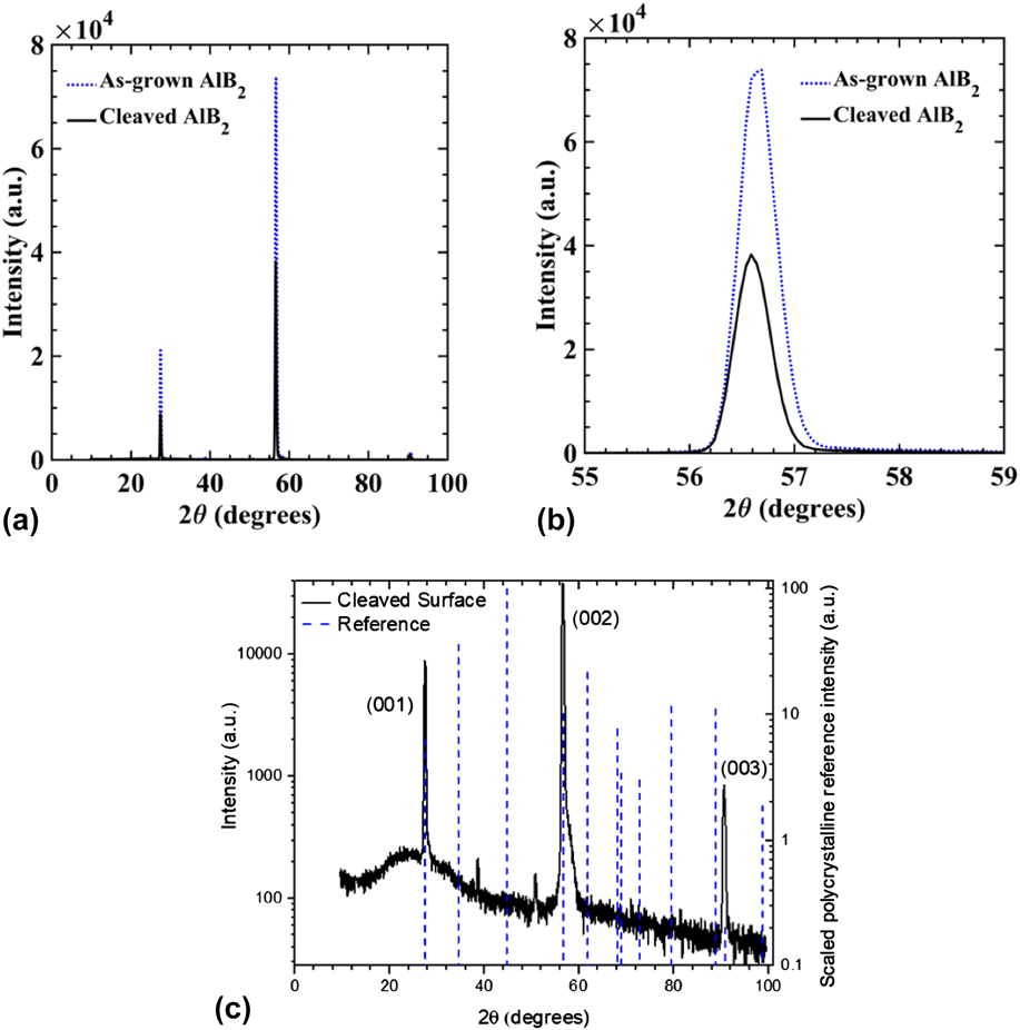
Figure 5(a) presents the XRD patterns obtained over the as-grown and cleaved AlB2 flakes. Figure 5(b) shows more single-crystalline surface for the cleaved flake, as shown by the sharper peak. Figure 5(c) shows a semilog scale for the cleaved surface with different crystallographic planes, which are labeled in the figure. The dashed lines represent the relative normalized polycrystalline peak intensities of AlB2, which are extracted from the literature.Reference Hofmann and Jäniche38 The cleaved plane showed only the diffraction peaks corresponding to the basal plane.
XRD for the as-grown and cleaved AlB2 flakes in (a and b) linear scale, and (c) log scale for the cleaved sample.

2. SIMS depth profiling
The oxidation of AlB2 via exposure in dry air or oxygen was investigated for the samples with main attention on the kinetics of oxidation and its growth rate. For the case of air exposure of the cleaved surface of the AlB2 monocrystal, there is an important question concerning the oxide layers, that is, how does the few nm thickness of the oxide layer change with the time of oxidation? The kinetics of the oxidation growth rate is important to ensure the stability of the cleaved surface before the successive chemistry on the surface, such as the deposition of epitaxial thin films.
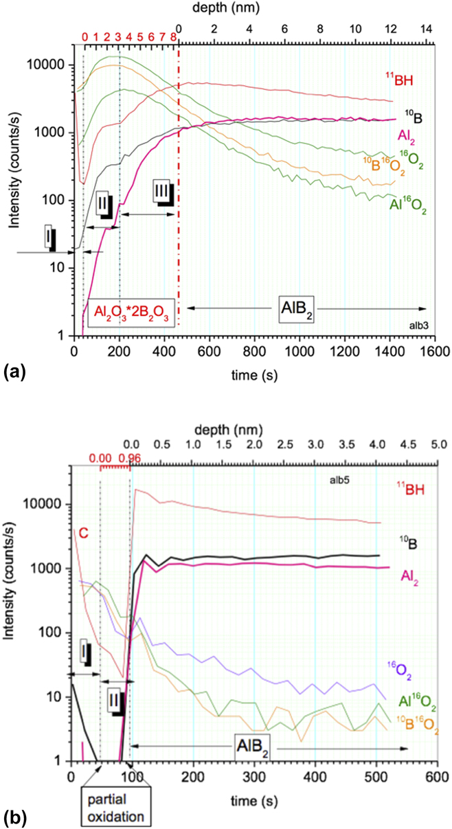
To gain further insight about the compositional analysis of AlB2 flakes as a function of depth, SIMS CAMECA 4F was used for depth profiling. The angle of incidence of the beam was 26°. The measured secondary ions were negatively charged. Three different areas of each sample were probed. The profiles for these areas were very similar and are shown in Fig. 6. The SIMS characterization included both the as-grown and cleaved flakes. The purpose of characterizing the as-grown flake was to show the effect of cleavage on the surface roughness and oxidation.
Quantitative SIMS depth profiles of (a) as-grown AlB2 and (b) cleaved AlB2 flakes.

Within the first 35 s of profiling the as-grown AlB2 sample shown in Fig. 6(a), the surface contamination was removed (Zone I). The transition zone, Zone II, was characterized by increasing the concentration of Cs (delivered from the beam), which increased the ionization probability of the emitted ions. It means that increasing of the signals of ions in this zone did not match with the increasing concentration of the corresponding oxides. Zone III showed decreasing concentration of oxides, with increasing B and Al. The next zone was the profiling of the bare AlB2 (the signals of B and Al are steady).
The observed high signals of AlO2 and BO2 indicated strong oxidation, thus the topmost layer likely consisted of oxidation states for Al and B such as Al2O3 and B2O3. Previously, the oxidation kinetics of AlB2 were investigated for the powders which were heated in air (10° C/min).Reference Whittaker, Sohn and Cutler39 It was found that at temperatures >600 °C, the oxide products Al2O3 and B2O3 form Al4B2O9 (2Al2O3·B2O3) due to strong removal of B2O3. For the case presented in this work, the temperature of drying in air was 110 °C only, thus likely, the products of oxidation Al2O3 and B2O3 form Al2O3·2B2O3. Referring to Fig. 6, the top x-coordinate shows the profiling depth, which is calculated with the TRIM code, commonly used for sputtering (http://www.srim.org/). The profile shows that the native oxide layer was grown via exposure to atmospheric oxygen during the drying of the manufactured sample, which was inserted into a convection oven at 110 °C for 120 min. The depth profile showed that the thickness of the oxide layer was ∼8 nm. An interesting feature was the observation of the signal of BH. This signal was notable even at a depth of ∼15 nm in the AlB2 flake. It is likely that hydrogenation occurred at the time of synthesis of AlB2.
Next we consider the cleaved 2D AlB2 flake, which was exposed in air for 5 min after the mechanical cleavage. The profile of this sample was different. Within the first 40 s of profiling the cleaved sample shown in Fig. 6(b), the surface contamination (carbon, “natural boron”) was removed (Zone I). Zone II showed the decreasing concentration of oxides, with increasing B and Al. The next zone was the profiling of the bare AlB2 (the signals of B and Al are steady). The observed signals of AlO2 and BO2 indicated that the topmost molecular layer consisted of Al2O3 and B2O3 similar to the as-grown flake before the cleavage. However, the rapid decreasing of the signals of AlO2 and BO2 (∼5 times within 1 nm of profiling) showed that the degree of oxidation was reduced with the depth. The total thickness of the oxide layer was less than 1 nm [Fig. 6(b)]. One should note that the extended low intensity signals of Al2O3 and B2O3 (intensities decrease 100 times) at the depth >2 nm were due to the common diffusion effect stimulated by the beam of primary ions of 14.5 keV Cs+. Similar to the sample with a native oxide layer, an interesting feature was the observation of the signal of BH. This signal was notable even at a depth of ∼5 nm in the AlB2 flake. The sudden increase of signals of Al2 and 10B showed that the surface was very flat at the probing area which is of 500 × 500 µm2. Therefore, the results of SIMS depth profiling support the findings of AFM roughness imaging.
C. Epitaxial thin film growth
To demonstrate the superior surface of cleaved AlB2, ALD was used to deposit a TiO2 film with a thickness of 10 nm. Also, silicon on insulator (SOI) is used for TiO2 deposition, for comparison. Silicon is a common substrate for the growth of epitaxial thin films especially in semiconductor manufacturing. SOI refers to a layered structure of the thin silicon film (∼200 nm), top of the insulator (1000 nm thick SiO2 layer), and finally the micro-thick Si wafer substrate. The Si wafer was cleaned with acetone and methanol successively using an ultrasonic cleaner. Hot air was used to dry the Si between both solutions. The silicon was used for deposition without any further etching of the native SiO2 oxide. The aim of this experiment was to understand how the superficial oxide layer of cleaved 2D AlB2 and Si would influence the growth of an epitaxial thin film.
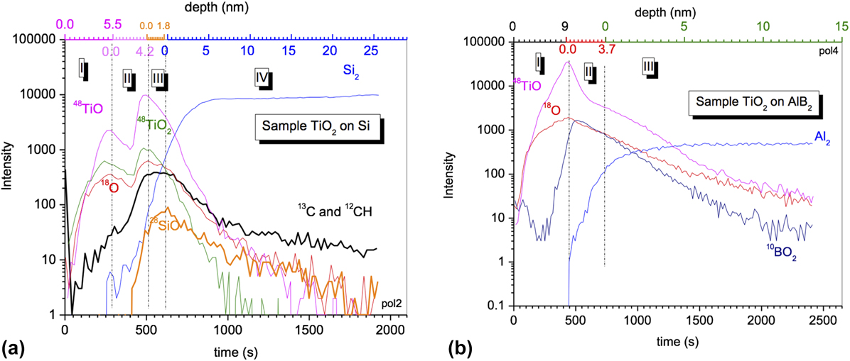
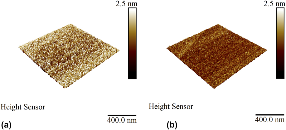
To evaluate the quality of the epitaxial growth of the TiO2 film on both AlB2 and Si, SIMS depth profiling and AFM topography imaging were used, as shown in Figs. 7 and 8, respectively. SIMS showed four distinct layers for the TiO2/Si sample, where two of them were titanium oxide layers. The first layer (area I) was the pure TiO2 film, while the second layer (area II) consisted of titanium oxide with a strong content of the carbon (perhaps hydrocarbons). The third layer was the silicon oxide with a strong content of the carbon as well. The fourth layer (area IV) is the pure Si film. The estimated thicknesses of the layers are presented as the X coordinate at the top of the graph. On the other hand, three notable profile areas were observed for the TiO2/AlB2 sample. Area I showed the TiO2 layer of thickness ∼9 nm. The second area was the thin natural oxide layer of AlB2 with a thickness of ∼3.7 nm. Area III was the body of the AlB2 substrate. The AFM images were used to measure the R q roughness (see Fig. 8). The roughness was 2.6 and 5.4 Å for the TiO2 thin film on both AlB2 and Si substrates, respectively. The TiO2 thin film grown on AlB2 was smoother as compared to the one grown on silicon. This was due to two reasons: (i) the cleaved AlB2 had smaller surface roughness than Si and (ii) cleavage removed the majority of AlB2 surface defects. Therefore, cleavage improved the conditions of the AlB2 surface for epitaxial thin film growth.
Quantitative SIMS depth profile and AFM roughness images of epitaxial grown (a) TiO2/Si and (b) TiO2/cleaved AlB2.

AFM roughness images of the TiO2 film deposited on the (a) silicon substrate and (b) cleaved AlB2 surface.

IV. CONCLUSION
To achieve the growth of high-quality epitaxial thin films, the substrate needs to be smooth and flat at the atomic level, highly single crystalline, and has a stable and low degree of oxidation. The cleaved AlB2 was found to successfully attain these requirements. The as-grown AlB2 flake had substantial defects and evidence of intermetallic formation. The cleavage of the AlB2 flake yielded the surface layer more single crystalline. In addition, the cleaved AlB2 flakes had a surface roughness that was lower than the lattice parameter c of the AlB2 phase and showed enhanced mechanical properties. Using SIMS, we were able to characterize the oxide surface and subsurface of AlB2 at the nanoscale. The as-grown flake had a native oxide layer with a thickness of ∼8 nm. This oxide layer consisted of Al2O3 and B2O3. The cleavage resulted on a 2D AlB2 with a superficial oxide layer with an average thickness of ∼1 nm. The oxide layer was stable after cleavage as shown by AFM and SIMS, providing sufficient time to carry out thin film deposition, taking advantage of the atomic-scale ultra-smooth and flat surface. TiO2 thin film deposition showed that the cleaved AlB2 can be a promising 2D material for thin film epitaxial growth.
ACKNOWLEDGMENTS
The authors acknowledge the use of the Materials Characterization Facility (MCF) at Texas A&M University and the Frederick Seitz Materials Research Laboratory (MRL) at the University of Illinois at Urbana–Champaign. The authors acknowledge the help of Mete Bakir in the XRD characterization of the flakes. Part of this study was funded by NSF Grant No. CHE-1308312.