I. INTRODUCTION
In the last years, the chipless technology has been experiencing an increasing interest as enabling technology for the Internet of Things (IoT) paradigm. The breaking through concept at the base of the chipless radio frequency identification (RFID) approach is that in order to realize extremely low-cost, highly ecofriendly, additive manufacturing compatible, and flexible tags for the widest “object” compatibility, wireless transmission of information, and sensing capabilities should be pursued by getting rid of the inherent limitations of using integrated monolithic circuits for memory storage or signal processing [Reference Preradovic and Karmakar1, Reference Kim, Mariotti, Alimenti, Mezzanotte, Georgiadis, Collado, Roselli and Tentzeris2].
On the one hand, the challenge of chiplessly encoding and transmitting information has led to the development of several tag designs, which can be classified into three main categories depending on the adopted coding strategies: the most traditional time-domain reflectometry (TDR) [Reference Nair, Perret and Tedjini3, Reference Hu, Zhou, Law and Dou4], where the tag receives a pulse-signal and transmits back a train of pulses delayed by a predefined time, the spectral signature-based technique [Reference Islam, Yap, Karmakar and Azad5, Reference Vena, Perret and Tedjini6], where the tag encodes the data into the spectrum by means of resonant structures, and the harmonic radar-based technique [Reference Lazaro, Villarino and Giribau7–Reference Mariotti, Alimenti, Virili, Orecchini, Mezzanotte and Roselli9], where the tag receives a signal at a fundamental frequency and re-transmits it back at the second harmonic by means of non-linear components. In fact, the chipless tag category also includes tags with discrete components in package [Reference Dionne, Matbouly, Domingue and Boulon10, Reference Girbau, Ramos, Lazaro, Rima and Villarino11].
On the other hand, the chip removal has enabled and fostered the diffusion of new concepts and circuit fabrication techniques, such as printing electronics [Reference Subramanian, Frechet, Chang, Huang, Lee, Molesa, Murphy, Redinger and Volkman12], ink-jet printing, aerosol-jet printing [Reference Thompson and Yoon13], roll-to-roll, glued electronics [Reference Alimenti, Mezzanotte, Dionigi, Virili and Roselli14], which have paved the way to circuit fabrication on unconventional substrates, like polyethylene terephthalate, textiles, cellulose, cork, and plenty of materials never adopted for electronics before.
In this scenario, the potential of the cellulose as a paradigmatic substrate for electronics is becoming even more evident [Reference Steckl15]. In fact paper, being extremely lightweight, flexible, biodegradable, and intrinsically inexpensive, allows RFID fields of application to be broadened by developing low-cost and versatile tag solutions, while reducing the waste volume related to the widespread diffusion of electronic apparatuses into the environment. Although paper features some drawbacks, such as high dielectric losses, surface roughness, lack of ruggedness, and an unstable relative permittivity mainly with respect to humidity variations, there are some applications where it is a natural fit, such as, for instance, microfluidics [Reference Wenjing, Cook, Tentzeris, Mariotti and Roselli16], where its porosity can play a key role.
The aim of the present work is to exploit what is broadly considered to be one of the main drawbacks of the paper substrate, namely its fragility, as a useful characteristic: a wireless crack sensor for sealing purposes has been designed and a proof of concept has been carried out. The paper is organized as follows: in the two next sections a brief description of the adopted copper (Cu) laminate technology (Section II) and an analysis of the harmonic radar-based approach (Section III) are given; then in Section IV, the performance of a harmonic one-bit tag are reported and finally the design and prototyping of the crack sensor is described (Section V).
II. TECHNOLOGY AND MATERIALS
The circuits proposed in this work have been fabricated by means of the Cu laminate technique, which has already stated and demonstrated in several RF and microwave circuits [Reference Alimenti, Mezzanotte, Dionigi, Virili and Roselli14–Reference Mariotti, Alimenti, Mezzanotte, Dionigi, Virili, Giacomucci and Roselli17]. This method consists of the shaping of an adhesive Cu tape by standard photolithography and the application of the Cu pattern on the paper substrate by means of a sacrificial layer. The photographic paper used for the circuit fabrication is a 230-µm thick sheet from Mitsubishi™, having a dielectric constant (ε r ) of about 3 below 10 GHz and a loss tangent (tanδ) of 0.08, while the adhesive Cu tape is from 3M™.
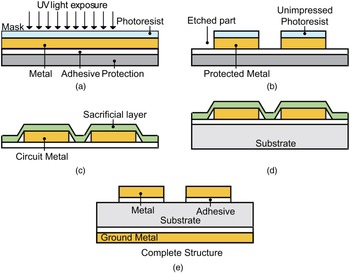
Figure 1 illustrates all the steps of this technique. Since a thin glue layer is interposed between each metal and the paper substrate as well as among paper substrates often required to keep control of the whole composite dielectric thickness, a multilayer structure is thus obtained. In [Reference Mariotti, Alimenti, Mezzanotte, Dionigi, Virili, Giacomucci and Roselli17], an equivalent uniform substrate is defined and its parameters are reported.
Cu laminate technology: photoresist deposition and UV light exposure (a); wet etching (b); transferring of the Cu pattern on the paper substrate by a sacrificial layer (c, d); and fabrication of the ground plain with a slab of Cu tape (e).

This technique, relying on a chemical procedure (which can be avoided by directly shaping the circuit layout with a laser-cutter machine) and a subtractive approach, can be considered more traditional than the other techniques conceived to fabricate circuits on paper, but it shows some interesting advantages, such as higher conductivity (σ cu = 5.8 × 10⁷ S/m), the possibility to solder surface mount components by means of conventional eutectic alloy, compatibility with printed circuit board (PCB) fabrication equipment, which make it a valuable complementary approach with respect to printing electronics.
III. HARMONIC TAG
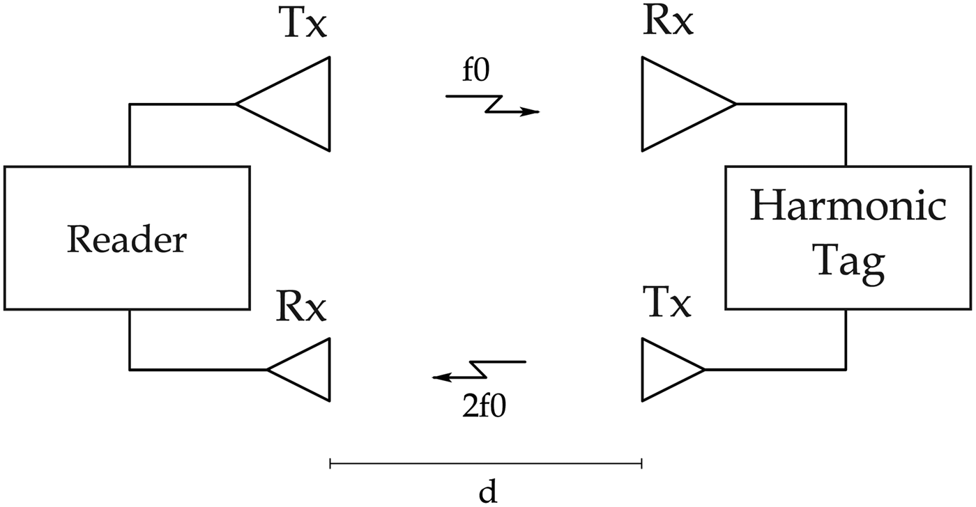
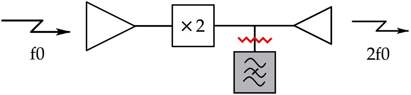
As already stated, a harmonic tag is based on the harmonic radar principle, according to which the tag converts the incoming signal at fundamental frequency to the second harmonic in order to efficiently separate the uplink at f 0 from the downlink (2f 0) and provide full insensitivity to the environmental backscattering. A basic scheme is reported in Fig. 2. In order to perform the frequency conversion stage, at least a non-linear component on board is required. It means that at the moment a harmonic tag cannot be made completely printable or recyclable and this has a residual impact on the tag cost.
Harmonic tag working principle: the signal transmitted by the reader at f 0 is doubled by the tag, which returns back an answer signal at 2f 0 [Reference Palazzi, Alimenti, Mezzanotte, Virili, Mariotti, Orecchini and Roselli21].

However, unlike the other chipless categories, this approach is naturally immune to clutter returns and man-made noise, since the harmonic radar receiver is tuned to the second harmonic of the transmitter. Consequently, the design of one-bit tag is straightforward (see Section IV) and such a system can be employed in several applications within the IoT paradigm: logistics, packaging, safety, electronic article surveillance [Reference Aumann, Kus, Cline and Emanetoglu18]. On the other hand, this approach becomes more troublesome when multibit data have to be managed and the research in this field is far from the results obtained with the spectral signature-based approach (in [Reference Vena, Perret and Tedjini19] a coding capacity of 49 bit has been reached). An important issue to be considered is the operational bandwidth of the non-linearity employed for the frequency doubling, since it could represent a bottleneck for the coding capacity in the frequency domain. Nevertheless, a promising approach which is worth being mentioned is presented in [Reference Alimenti and Roselli20], where in a harmonic tag the information is encoded as the phase-difference between two signals transmitted in orthogonal polarization.
IV. ONE-BIT TAG
In passive harmonic tags, the non-linearity plays a key role, since it determines the efficiency with which the tag is capable of converting the fundamental tone into the harmonics and has an impact on the cost of the tag, which, when adopting a chipless technology, mainly depends on the number of commercial components employed. Therefore, in order to maximize the reading range of the system while keeping the cost very low, the frequency multiplication function has been performed by a passive frequency doubler, based on a single low barrier Schottky diode and designed to feature a low conversion loss at low-input power with a minimum component count.
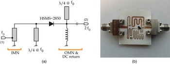
This design has already been described in [Reference Palazzi, Alimenti, Mezzanotte, Virili, Mariotti, Orecchini and Roselli21]. The schematic and the fabricated prototype are reported in Figs 3(a) and 3(b), respectively. The doubler is targeted for f 0 = 1.04 GHz. Such a frequency has been chosen to prove the system operation in the low GHz range. It has been experimentally demonstrated that the doubler shows a minimum conversion loss of 13.4 dB for an input power of −10 dBm, where the conversion loss is defined as the ratio of the available source power (P avs ) at f 0 to the output harmonic power at 2f 0 delivered to the load:
 $${C_l} = \displaystyle{{P_{avs}^{f0}} \over {P_{load}^{2f0}}} {\kern 1pt}. $$
Frequency doubler: schematic (a) and prototype manufactured in paper substrate (b). All the components, except for the diode and the capacitor in the output-matching network, are implemented as distributed elements in microstrip technology, which have been folded in order to reduce the area occupation. The Schottky diode is soldered on the Cu laminate as in standard PCBs. Active area: 18 mm in length and 19 mm in width [Reference Palazzi, Alimenti, Mezzanotte, Virili, Mariotti, Orecchini and Roselli21].

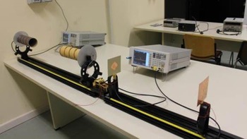
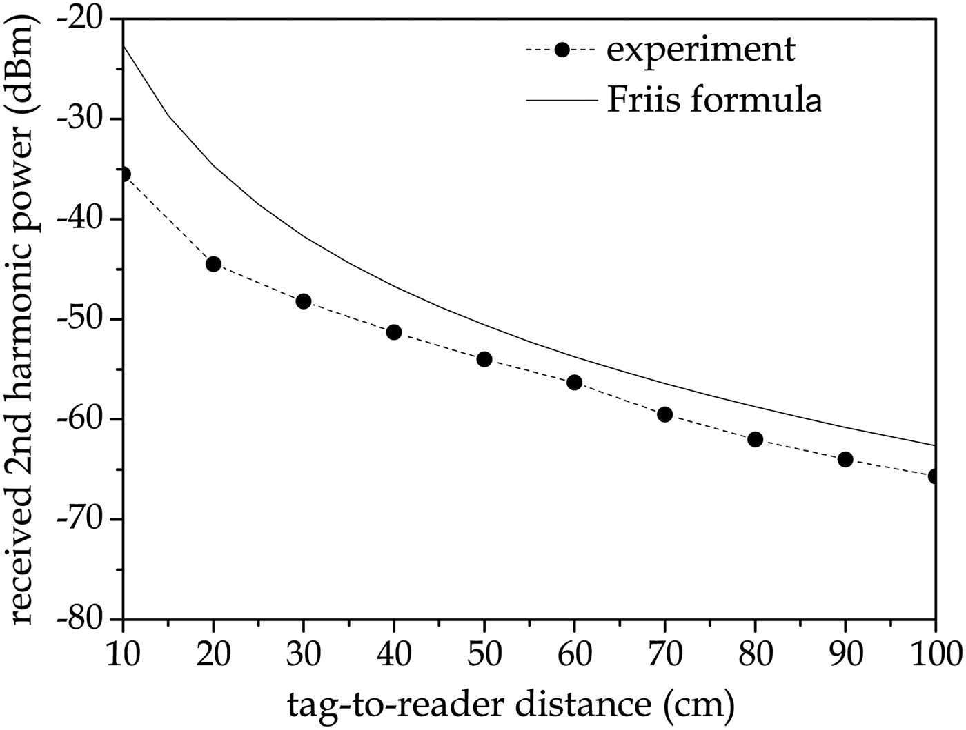
A harmonic one-bit tag has been assembled connecting the doubler to suitable antennas. The experimental setup is reported in Fig. 4. In the tag, a helix antenna (gain 4.9 dBi) is used at the fundamental frequency, while a patch antenna (gain 4.3 dBi) is adopted for the second harmonic. The reader antennas are equal to the tag ones. Note that these values of antenna gain are typical for many RFID systems. The reader transmitter has been implemented with a HP8657A source and the receiver was an Agilent N9320B spectrum analyzer. The transmitted power has been set to 10 dBm, whereas the tag-to-reader distance has been varied in a range between 10 and 100 cm. Figure 5 shows the measured power as a function of distance and compares the experimental results obtained in a laboratory room with no special anechoic provisions to a calculated curve based on a link budget analysis. In particular, the received power has been theoretically estimated according to the following formula:
 $${P_{RX}} = \displaystyle{1 \over 4}{P_{TX}}2{G_1}2{G_2}{C_g}{G_c}{\left( {\displaystyle{{{\lambda _0}} \over {4\pi d}}} \right)^4}.$$
One-bit harmonic RFID system: experimental setup. The wireless up-link at f 0 has been implemented with helix antennas, whereas the down-link at 2f 0 has been implemented with patch antennas.

Harmonic RFID experiment: received signal power versus tag-to-reader distance d. The experiment is in good agreement with the link-budget analysis based on the Friis’ formula. Similarly to radar, the received power decays as 1/d 4.

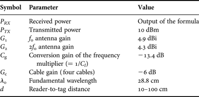
The meaning and the value associated to each symbol are reported in Table 1. This equation takes into account that f 0 and 2f 0 antennas are identical for the reader and for the tag. Note that the 1/4 coefficient is due to the fact that the tag-to-reader communication happens at 2f 0 (i.e. twice the fundamental frequency f 0 used for the reader-to-tag link) and the calculation is made on the assumption of a constant conversion loss of 13.4 dB, which corresponds to the actual value only for a distance of approximately 65 cm. As can be seen from the graph, it has been experimentally demonstrated that the tag-to-reader range extends beyond a distance of 1 m, since the received signal is well above the noise floor of typical receivers.
Legend of the link-budget formula.

By equating (2) with the radar equation, the harmonic radar cross-section (HRCS) can be extracted. This parameter plays the same role as the conventional RCS for the other chipless RFID systems and as a consequence it represents a useful figure of merit. Thus, from:
 $${P_{RX}} = \displaystyle{1 \over 4}{\kern 1pt} \displaystyle{{{P_{TX}}{\kern 1pt} {G_1}{\kern 1pt} {G_2}{\kern 1pt} {\sigma _h}{\kern 1pt} \lambda _0^2} \over {{R^4}{{(4{\kern 1pt} \pi )}^3}}}{\kern 1pt}, $$
where the 1/4 coefficient accounts for the receiver which is tuned to 2f 0, the HRCS is given by:
 $${\sigma _h} = {G_1}{\kern 1pt} {G_2}{\kern 1pt} {C_g}({P_{avs}}){\kern 1pt} \displaystyle{{\lambda _0^2} \over {4\pi}}. $$
A similar approach is described in [Reference Colpitts and Boiteau22]. Using the values reported in Table 1, an estimate of the HRCS of the proposed tag can be found:
 $${\sigma _h} = - 26\,{\rm dBsm}.$$
It is worth noticing that, unless conventional RCS, the HRCS is distance-dependent, since it depends upon the conversion loss, which in turn varies according to the available power at the input of the doubler.
V. CRACK SENSOR
The proposed tag is intended for those scenarios where an even huge population of tagged objects is present and the aim is to automatically reveal if one of them has been tampered. This can be helpful to speed up goods monitoring in supply chains and as security system in retail. To this end, the tag is based on a disposable band-stop filter and operates according to an invert-logic (Fig. 6).
Schematic representation of the developed disposable crack sensor.
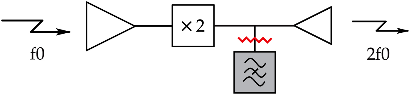
In fact, in quiescent condition, the tag does not re-radiate a signal when interrogated (referred to as “intact condition” in the following), since the second harmonic generated by the frequency doubler is short-circuited by the band-stop filter at the output side. But when the filter is torn off (referred to as “cracked condition” in the following), the output signal can reach the transmitting antenna, thus causing an alarm.
Such a sensor can also be employed to reveal the increase of a crack in a material as well as the tampering of envelops or boxes of interest: for instance official letters for public contests or packages containing precious items. The reader could be a portable instrument, used before the start of a public exam or before the shipping of a box as a security control.
Considering that a quarter-wave open-circuited stub behaves as a series resonant circuit, the band-stop filter can be implemented by inserting such stubs in shunt along a transmission line, provided that the stubs are separated by quarter-wave sections of line, which act as admittance inverters, capable of converting alternate shunt resonators to series resonators.
For the presented application the filter has to be designed with the aim of maximizing its attenuation at the second harmonic (2f 0), without affecting the fundamental frequency (f 0). Thanks to these loose requirements (its fractional bandwidth can approach to 2), a simple second-order Butterworth filter has been employed. The characteristic impedances of the stubs are given by Pozar [Reference Pozar23]:
 $${Z_{0n}} = \displaystyle{{4{Z_0}} \over {\pi {g_n}\Delta}}, \;n = 1,2,$$
where g
n
are the impedance-scaled prototype elements and Δ is the fractional bandwidth. By choosing Δ = 2, the characteristic impedance for both stubs is equal to
 $22.5{\kern 1pt} \,\Omega $
, which corresponds to a line width of about 2.5 mm.
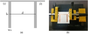
To validate the proposed circuit, the layout of the filter has been fabricated using the previously mentioned technique based on the Cu adhesive laminate and the paper substrate. The circuit design has been carried out by exploiting the electromagnetic solver CST Studio Suite™. The material parameters are quoted in [Reference Mariotti, Alimenti, Mezzanotte, Dionigi, Virili, Giacomucci and Roselli17], whereas the circuit parameters are reported in the caption of Fig. 7.
Layout of the filter (a) and prototype manufactured in paper substrate (b). The band-stop filter is composed of two open-circuit stubs, a quarter wave long at 2f 0, spaced by a quarter wave. The main circuit parameters are: lo = 24.9 mm, wo = 2.5 mm, and d = 22.3 mm.

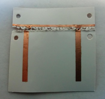
If the stubs in shunt are removed (Fig. 8) the circuit becomes a simple
 $50{\kern 1pt} \,\Omega $
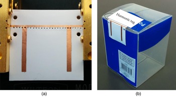
line, thus losing its filtering function. In order to ease the stub removal and to guarantee that, in case of tampering, the stubs would be completely removed, a series of equi-spaced holes has been fabricated (Fig. 9(a) shows the filter with holes; whereas (b) represents an example of a possible application).
Band-stop filter prototype after the stub removal.

Band-stop filter prototype with holes (a) and example of a possible application (b).

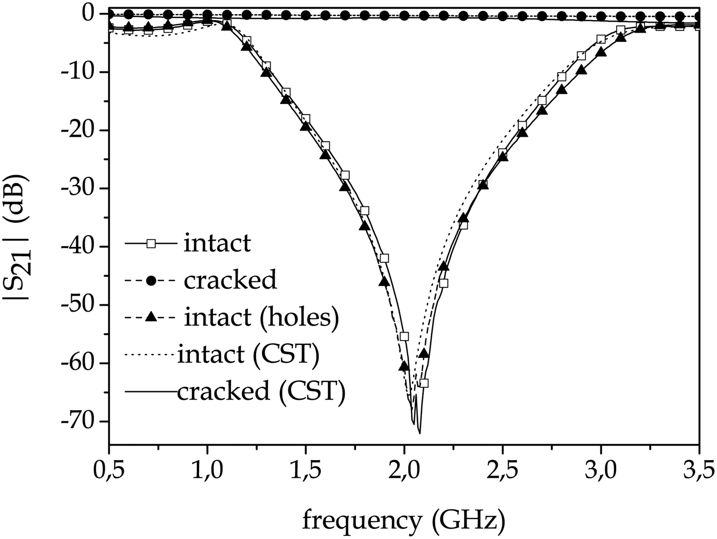
The transmission coefficient of the disposable band-stop filter is reported in Fig. 10, where a comparison between simulation and measurement is made. The circuit testing has been conducted by means of the vector network analyzer PNA N52230A from Agilent. At the input frequency (2.08 GHz) a variation of more than 60 dB in the transmitted power has been experimentally demonstrated. It is worth noticing that after the stub removal a good matching between the input and the output ports of the circuit under test is experienced (|S 21| = −0.5 dB) and the signal is allowed to pass toward the output antenna. In Fig. 10, the transmission coefficient of the filter with holes is also reported and it is demonstrated that holes do not significantly affect the filter performance.
Comparison between simulation (a) and measurement (b) in terms of transmission coefficients. When the filter is intact, it causes an attenuation of 65 dB on the incoming signal at 2.08 GHz, whereas when the filter is cracked the attenuation introduced is of about 1 dB.

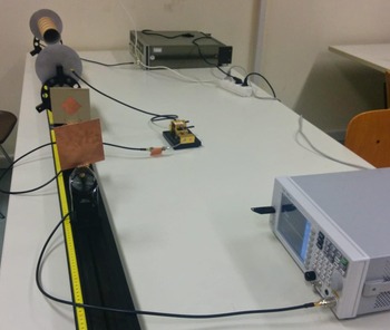
In order to assess the performance of the whole tag in an actual environment with respect to its distance from the reader, a suitable experiment has been set up. In Fig. 11, the block diagram of the adopted test bench is reported: a generator, implemented with a HP8657A source and set to 1.04 GHz, is connected to the transmitting antenna at f 0; the wireless signal is received by the receiving antenna of the tag, followed by the frequency doubler described in Section IV. The latter is connected to the proposed disposable filter, which is in turn connected to the tag transmitting antenna at 2f 0. Finally, the receiving antenna of the reader is connected to an Agilent N9320B spectrum analyzer. All the connections have been made by means of standard cables.
Measurement chain, in order from the background: a HP8657A generator, a wireless link at f 0, a frequency doubler, the crack sensor, a wireless link at 2f 0, and a N9320B spectrum analyzer from Agilent.

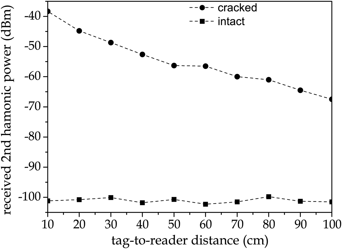
Figure 12 reports the power measured by the spectrum analyzer versus the tag-to-reader distance for an available input power of 10 dBm supplied by the generator at the input frequency 1.04 GHz. The noise floor of the receiver is of about −100 dBm. For a minimum distance of 10 cm the variation in the received power when the filter is intact or cracked is of about 60 dB, thus proving the high dynamic rage of the sensor. Since the received power for the cracked condition decreases with the distance, the intact-to-cracked range decreases as well. Nevertheless, at 1 m the difference in the received power is about 30 dB, thus demonstrating that the two conditions are still well noticeable.
Harmonic RFID experiment: received signal power versus tag-to-reader distance d when the filter is intact and when cracked.

The measurements presented in this paper have been conducted by guaranteeing the alignment between the tag and the reader antennas. Nevertheless, by choosing circular polarized antennas for the reader and linear polarized antennas for the tag, the tag-to-reader orientation issue can be relaxed, at the expense of 6 dB of losses (3 dB for the uplink and 3 dB for the downlink).
Moreover, in order to separate the tag responses and automatically identify the tampered item, spatial separation with the help of a narrow beam reader antenna is a suitable solution. If a semi-automatic approach is still acceptable, then the crack sensor can be used to reveal when tampering happens, while the item identification can be done by visual inspection.
Finally, a comparison with other crack sensors, reported in Table 2, underlines the originality and the robustness of the proposed approach.
State-of-the-art.

VI. CONCLUSIONS
A one-bit harmonic tag working as crack sensor has been presented and the idea has been experimentally demonstrated. A description of the adopted technology has been included together with a report about the harmonic approach. The sensor, based on a disposable band-stop filter, has demonstrated a maximum dynamic range of 60 dB, whereas it is still capable of working for tag-to-reader distances greater than 1 m, where it exhibits a dynamic range of 30 dB.
ACKNOWLEDGEMENTS
The authors are grateful to Keysight Technologies and Computer Simulation Technologies for the donation of the ADS and CST software licenses respectively. This work was partly supported by the research project “Green Tags and Sensors with Ultrawideband Identification and Localization Capabilities” (MIUR, 2011).
 Valentina Palazzi was born in Spoleto, Italy, in 1989. She received her M. S. degree in Electronic Engineering (magna cum laude) from the University of Perugia, Italy, in February 2014, where she is currently attending the Ph. D. program in Industrial and Information Engineering with the High Frequency Electronics (HFE) Lab. In the summer 2015 she was Visiting Ph.D. Student at Tyndall National Institute, Ireland. Her research interests concern the design of chipless RFID with sensing capabilities, radar front-ends, wireless power transfer technologies, and green electronics.
 Chiara Mariotti was born in Assisi (Italy) in 1987. She received her Laurea degree (magna cum laude) in Electronic and Telecommunication Engineering from the University of Perugia (Italy) in November 2011. In spring 2012, she joined the ATHENA Research Group (Georgia Institute of Technology, Atlanta, USA) for 6 months, working on ecocompatible indoor localization systems and other types of sensors fabricated by means of inkjet printing technology. In 2013, she started the Ph. D. with the High Frequency Electronics (HFE) Lab at the University of Perugia working on green technologies for passive and energetically autonomous RFID tags. At the end of 2013, she joined again for 6 months the ATHENA Research Group to work on multi-layers inkjet printed systems and devices such as passives and microfluidics sensors.
 Federico Alimenti received his Laurea and his Ph. D. degrees from the University of Perugia, Italy, in 1993 and 1997, respectively, both in Electronic Engineering. In 1996, he was a recipient of the URSI Young Scientist Award and Visiting Scientist at the Technical University of Munich, Germany. Since 2001, he has been with the Department of Engineering at the University of Perugia teaching the class of Microwave Electronic. Between 2011 and 2014 he was the scientific coordinator of the ENIAC ARTEMOS project. In 2013, he was the recipient of the IET Premium (Best Paper) Award and the TPC Chair of the IEEE Wireless Power Transfer Conference. In the summer 2014, he was Visiting Professor at EPFL, Switzerland. His interests are about microwave circuit design. He has authored a European Patent and more than 150 papers in journals and conferences. Federico Alimenti (H-index equal to 11, Scopus) is Senior IEEE Member.
 Marco Virili was born in Terni, Italy, in 1983. He received his Master of Science in Electronic Engineering from the University of Perugia, Italy, in 2009. Since 2010, he has been with the Department of Engineering (DI), University of Perugia, as an RF designer. In 2011, he started the Ph. D. course in Information Engineering with the High Frequency Electronics (HFE) of the same university. In 2013, he spent 1 month in the Department of Information Technology (INTEC) of Ghent University, Belgium, with the COST Short Term Scientific Mission (STSM), working on wearable electronic. In 2014, he joined the Centre Tecnològic de Telecomunicacions de Catalunya (CTTC), Spain, as Ph. D. visiting student for 6 months working on microwave devices for WPT and EH. Since 2014, he has been an IEEE Student Member.
 Giulia Orecchini received her Laurea degree in Electronic Engineering from the University of Perugia, Italy, in 2008 and her Ph. D. degree in Electronic and Information Engineering from the same University, in 2012. During her Ph. D. studies she joined the ATHENA Research Group, Georgia Institute of Technology, Atlanta. Her research interests concern the development of RFID electronic systems and technologies. She is currently working as a research assistant at the University of Perugia.
 Paolo Mezzanotte was born in Perugia, Italy, in 1965. He received his Ph. D. degree from the University of Perugia, Italy, in 1997. Since January 2007, he is an Associate Professor with the same University, teaching the classes of Radiofrequency Engineering. His research activities concern numerical methods and CAD techniques for passive microwave structures and the analysis and design of microwave and millimeter-wave circuits. More recently his research interests were mainly focused on the study of advanced technologies such as LTCC, RF-MEMS, and microwave circuits printed on green substrates. These research activities are testified by more than 100 publications in the most important specialized journals and at the main conferences of the microwave scientific community. The present H-index of Paolo Mezzanotte (ISI journals) is equal to 13.
 Luca Roselli (M92 SM01), MG in 1988. In 1991 he joined the University of Perugia, where he is presently teaching Applied Electronics and coordinating the HFE-Lab as an Associate Professor. In 2000, he founded the spin-off WiS Srl. Since 2008–2012, he had been the member of the BoD of ARTsrl. He organized the VII CEM-TD-2007 and the first IEEE-WPTC-2013. He is member: of the list of experts of Italian Ministry of Research, of the IEEE Technical Committees MTT-24 (past chair), -25 and -26; of the ERC Panel PE7, of the AC of IEEE-WPTC and chairman of the SC-32 of IMS. He is involved in the boards of several International Conferences and he is reviewer for many international reviews (including IEEE-Proceedings, -MTT and -MWCL). His research interest is HF electronic systems, with special attention to RFID-NFC, new materials and WPT. He published more than 220 contributions (HFi 21, about 1700 citations – Scholar).