Introduction
Crossovers are critical building components in many applications, such as power distribution networks, Butler matrices, and beam-forming networks in phased array antennas [Reference Qin, Chen and Xiang1–Reference Palazzi, Alimenti, Mezzanotte and Roselli5]. The crossover is a four-port network with two crossed signal paths with no mutual interference in between. Thus, two isolated channels are created [Reference Bahl6]. The significance of the isolation level scales directly with the input power level to the crossover. For low-power RF signals, the leakage signal to the adjacent channel is often insignificant. However, in high-power RF applications, poor isolation allows a portion of the primary signal to couple into the adjacent channel with relatively high-power levels, causing severe interference. Therefore, when dealing with high-power RF applications, crossovers must provide both high-power handling capability and relatively high-isolation levels between channels. In this context, Substrate Integrated Waveguide (SIW) cavities can provide the high-power handling capability, but the high-isolation levels between channels are related to the structure of the crossover itself.
Several crossovers, based on SIW technology, have been reported [Reference Zhang, Zhou, Kai-Da, Yang, Sun, Bin, Tam, Feng, Tang and Hong7–Reference Han, Zhou, Zhang, Zhou and Wen13]. In [Reference Zhang, Zhou, Kai-Da, Yang, Sun, Bin, Tam, Feng, Tang and Hong7], the coupling between full and quarter modes SIW square cavities is used to obtain a wide stop-band response crossover with an in-band isolation level of 21.6 dB. In [Reference Zhou and Wu8], an over-mode, dual-mode SIW rectangular cavity is coupled with multiple single-mode cavities to tune the bandwidth of the channels. The crossover achieves an isolation level of 21.8 dB. In [Reference Sun, Deng, Xue, Zhu and Xing11, Reference Han, Zhou, Zhang, Zhou and Wen13], crossovers are reported using a centered square cavity, surrounded by additional four ones, with 36 dB and 30 dB isolation levels, respectively. Although all the previously reported works were realized using the SIW technology, which is capable of handling high input power levels, no power handling measurements are reported. Moreover, all these works have relatively low isolation levels (below 36 dB), which may not be sufficient for many high-power applications. In [Reference Lai, Yang, Chi and Ruimin14], the crossover response is realized by controlling the inter-resonating coupling between four evanescent-mode cavity resonators using varactor diodes, achieving an isolation of 20 dB. Although the structure has a small circuit size, the used active devices (varactors) prevent it from handling high input power levels. Moreover, the used biasing network increases the circuit’s complexity.
Compared to previously reported SIW filtering crossovers, this work proposes SIW crossover cavities that particularly target the realization of substantially higher isolation levels while maintaining compact size and high-power handling capability. The proposed SIW crossover cavities are based on two non-degenerate evanescent modes whose resonant frequencies are intentionally aligned through capacitive loading, rather than relying on symmetry-protected degenerate modes or multi-cavity implementations. The proposed structure consists of two stacked substrates that act as one evanescent mode circular SIW cavity. The electric fields of the excited evanescent modes are confined in the secondary substrate, while most of their magnetic fields exist in the main substrate, where the majority of the inductance of these modes exists. The SIW cavity hosts two crossed pairs of capacitive-loaded semicircular posts, as in [Reference El-Gendy, Khater, Abdelaziem, Abdalla, Peroulis and Hagag15, Reference El-Gendy, Khater, Abdalla, Peroulis and Hagag16]. Each pair excites an evanescent higher-order mode, with the magnetic fields of each pair being orthogonal to each other. The loaded capacitances define the resonant frequency of the excited modes. For the two pairs and at the same loading capacitances, the two orthogonal modes are excited at the same resonant frequency. Accordingly, two isolated channels are created. The isolation between channels is controlled through a number of slots in the top metal layer of the main substrate. Accordingly, the resonant frequency of the proposed SIW cavity crossover and the isolation between its channels are independently tuned. The presented SIW crossover cavity is realized at 8.7 GHz, with a good agreement between simulated and measured results. The crossover handles a measured input power up to 44.7 dBm (29.5 W), with a measured insertion loss of 1.7 dB. Moreover, a high isolation of 64 dB is measured between channels using a one-pole resonator. In addition, the scalability of the proposed one-pole crossover to a second-order transfer function configuration is demonstrated through EM simulations.
It is worth mentioning that both the proposed work and our prior work [Reference El-Gendy, Khater, Abdelaziem, Abdalla, Peroulis and Hagag15] are based on the concept of multi-mode cavity structures. However, the objectives, components, and functionalities presented in the two works are fundamentally different. In [Reference El-Gendy, Khater, Abdelaziem, Abdalla, Peroulis and Hagag15], the authors proposed switching structures, including DPDT (double-pole double-throw) and routing cavity switches, which exploited the modal behavior of multi-mode cavities to realize reconfigurable signal routing between different ports. These designs focused on dynamically switching signal paths using PIN-diodes. On the other hand, the proposed work introduces a crossover cavity structure, which is a distinct and novel component with a different operational principle and application. The focus here is not on switching or reconfiguration, but rather on simultaneous power transfer across intersecting transmission paths while maintaining a controlled isolation between them, achieved through a deliberate separation of the electric and magnetic field concentrations across two stacked substrates.
Theoretical analysis
Crossover circuit with limited isolation level
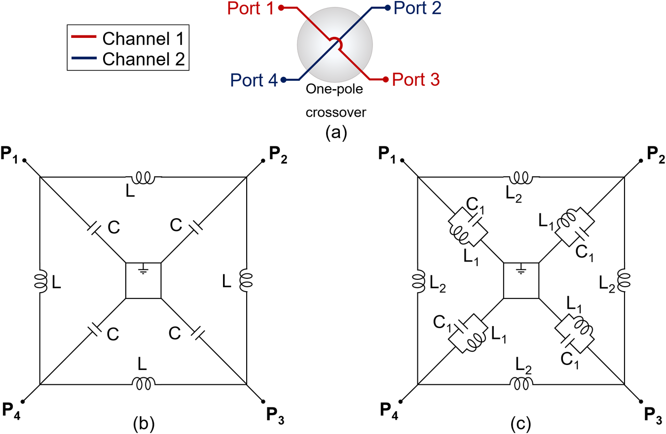
A diagram of a crossover with two isolated channels is shown in Fig. 1(a). The input signal from port 1 is coupled to port 3, expressing channel 1. In addition, the signal path between ports 2 and 4 forms channel 2. A conventional crossover circuit based on lumped elements [Reference Park, Lee, Lee, Kang and Jeon17, Reference Yu and Sun18], tested in circuit simulation, is shown in Fig. 1(b). Each port is connected with a shunt capacitor ( $C$). Also, each two adjacent ports are connected with a series inductor (
 $L$). The starting design shown in Fig. 1(b) is modified to have a better frequency response by replacing the lumped capacitors with LC tanks, as shown in Fig. 1(c).
For the crossover circuit with limited isolation. (a) A schematic. (b) A conventional circuit based on lumped elements. (c) A modified version by replacing the capacitances with LC tanks.

Figure 1 Long description
The image consists of three diagrams labeled (a), (b) and (c). Diagram (a) shows a schematic of a one-pole crossover with two isolated channels. Channel 1 connects Port 1 to Port 3 and Channel 2 connects Port 2 to Port 4. Diagram (b) illustrates a conventional crossover circuit with lumped elements. It includes four ports labeled P subscript 1, P subscript 2, P subscript 3 and P subscript 4. Each port is connected to a shunt capacitor labeled C. Adjacent ports are connected with series inductors labeled L. Diagram (c) shows a modified version of the crossover circuit, where the lumped capacitors are replaced with LC tanks. Each LC tank consists of an inductor labeled L subscript 1 and a capacitor labeled C subscript 1. The ports are similarly labeled as P subscript 1, P subscript 2, P subscript 3 and P subscript 4. Connections between ports are maintained with series inductors labeled L subscript 2.
 \begin{equation}
{K_e}={\frac{J_e}{\sqrt{Y_0 Y_r}}}
\end{equation}
The symmetrical form of the crossover equivalent circuit is shown in Fig. 2(a). The symmetry lines (AA’) and (BB’) are defined. It is worth mentioning that an admittance inverter ( $J_e$) is added at each port to express the external coupling of the circuit [Reference Hong and Lancaster19]. Using (1), the external coupling behavior is tuned using the external coupling coefficient (
 $K_e$), where (
 $Y_0$) and (
 $Y_r$) are the input port and resonator admittances, respectively. As in [Reference Pozar20], the admittance inverter (
 $J_e$) can be expressed as a
 $\pi$-network with a series capacitor (
 $C$), and two shunt capacitors (
 $-C$). To physically implement each lumped element, the circuit is expressed with shunt inductors (
 $L_e$) instead of the shunt capacitors (
 $-C$), as shown in the inset of Fig. 2(a). The values of the lumped elements of the admittance inverter (
 $J_e$) are calculated using (2).
 \begin{equation}
{C_e}={\frac{J_e}{\omega_0}}, \quad {L_e}={\frac{1}{\omega_0 J_e}}, \quad (\omega_0 = 2\pi f)
\end{equation}
For the crossover circuit with limited isolation. (a) The equivalent circuit defining the symmetry lines  $AA'$ and
 $BB'$, taking the external coupling into account. (b) Even-even mode circuit. (c) Even–odd/odd–even mode circuit. (d) Odd–odd mode circuit.

Figure 2 Long description
The image A shows a crossover circuit with symmetry lines labeled A-A' and B-B'. The circuit includes four ports labeled P1, P2, P3 and P4, each connected to an admittance inverter labeled J subscript e. Between each pair of ports, there are inductors labeled L subscript 2 divided by 2 and capacitors labeled C subscript 1. The inset shows the admittance inverter J subscript e as a pi-network with a series capacitor C subscript 1 and two shunt inductors L subscript e. The image B shows an even-even mode circuit with port P1 connected to an admittance inverter J subscript e and an inductor L subscript 2 divided by 2. The image C shows an even-odd/odd-even mode circuit with port P1 connected to an admittance inverter J subscript e and an inductor L subscript 2 divided by 4. The image D shows an odd-odd mode circuit with port P1 connected to an admittance inverter J subscript e, an inductor L subscript 2 divided by 4 and a capacitor C subscript 1.
For the even–odd analysis and by taking port 1 as the input port, the even-even, the even–odd/odd–even, and the odd–odd reduced circuits are shown in Fig. 2(b)–(d), respectively. Then, the admittances seen from port 1 are retrieved as follows
 \begin{equation}
Y_{ee} =\frac{{J_e}^2}{\frac{j}{\omega} \left( \omega^2 C_1 - \frac{1}{L_1} \right)}
\end{equation}
 \begin{equation}
{Y_{e o,o e}} = \frac{{J_e}^2}{\frac{j}{\omega} \left( \omega^2 C_1 - \frac{1}{L_1} - \frac{2}{L_2} \right)}
\end{equation}
 \begin{equation}
Y_{oo} = \frac{{J_e}^2}{\frac{j}{\omega} \left( \omega^2 C_1 - \frac{1}{L_1} - \frac{4}{L_2} \right)}
\end{equation}
As seen in Fig. 2(a) and (c), the even–odd and the odd–even reduced circuits are identical. Accordingly, the even–odd and the odd–even admittances are the same (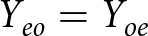 $Y_{e o}=Y_{o e}$). Given the concluded admittances and by using (6), the related reflection coefficients can be found [Reference Lin21], where (
 $Z_{0}$) is the impedance of the input port.
 \begin{equation}
{\Gamma_{e e, e o, o e, o o}}={\frac{1-Z_0 Y_{e e, e o, o e, o o}}{1+Z_0 Y_{e e, e o, o e, o o}} }
\end{equation}
Since the two channels are symmetric and to avoid redundancy, the S-parameters for channel 1 are retrieved as follows [Reference Collin22], taking into consideration that (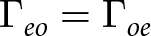 $\Gamma_{e o}=\Gamma_{o e}$).
 \begin{equation}
{S_{11}}={\frac{\Gamma_{e e}+2 \Gamma_{e o}+\Gamma_{o o}}{4} }
\end{equation}
 \begin{equation}
{S_{21}}={S_{41}=\frac{\Gamma_{e e}-\Gamma_{o o}}{4} }
\end{equation}
 \begin{equation}
{S_{31}}={\frac{\Gamma_{e e}-2 \Gamma_{e o}+\Gamma_{o o}}{4} }
\end{equation}
To achieve an ideal isolation between channels, the following condition should be satisfied.
 \begin{equation}
{\left|S_{21}\right|=\left|S_{41}\right|=0 \,\,\,\,\,\,\,\,\,\,\,\,\,\, (\omega=\omega_{0})}
\end{equation}
From (10) and by substituting in (8), we get
 \begin{equation}
{\Gamma_{e e}-\Gamma_{o o}=0}
\end{equation}
Also, for an ideal power flow through channels, the following conditions should be satisfied.
 \begin{equation}
{\left|S_{11}\right|=0 \,\,\,\, , \,\,\,\, \left|S_{31}\right|=1 \,\,\,\,\,\,\,\,\,\,\,\,\,\, (\omega=\omega_{0})}
\end{equation}
Considering that (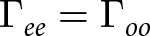 $\Gamma_{e e}=\Gamma_{o o}$) as from (11) and by substitution of (12) into (7) and (9), we get
 \begin{equation}
{1+\Gamma_{e o}=0}
\end{equation}
For an ideal response of the crossover circuit, the crossover should operate at the point where (11) and (13) are achieved concurrently.
The values of the lumped elements ( $L_{1}$,
 $L_{2}$, and
 $C_{1}$) define the resonant frequency of the proposed crossover circuit. As shown in Fig. 3(a) and at different values of the inductance (
 $L_{1}$), the resonant frequency decreases by increasing the capacitance (
 $C_{1}$), simulated at fixed values of (
 $L_{2}$). However, Fig. 3(a) may give the impression that the inductance (
 $L_{1}$) contributes less to the resonant frequency than (
 $C_{1}$), but it remains critical to resonance. Also, Fig. 3(b) shows that the resonant frequency decrements with the incrementing value of the inductance (
 $L_{2}$), simulated at pre-defined values of (
 $L_{1}$ and
 $C_{1}$). As observed in Fig. 3(a), the minimal variation of the capacitance (
 $C_{1}$) greatly shifts the resonant frequency of the proposed crossover. Consequently, the capacitance (
 $C_{1}$) plays the dominant role in tuning the resonant frequency of the presented crossover circuit. As shown in Fig. 3(a) and (b), the crossover circuit is tuned to operate at a resonant frequency of 8.7 GHz, with
 $L_{1}$,
 $L_{2}$, and
 $C_{1}$ values of 27.3 nH, 39.29 nH, and 0.04 pF, respectively. As shown in Fig. 3(c), the S-parameters of the crossover circuit are simulated at different values of the external coupling coefficient (
 $K_{e}$). As seen, increasing (
 $K_{e}$), the resonance becomes broader, the amount of power reflected at the resonant frequency decreases, and the isolation level between the channels decreases. This behavior reflects the fact that stronger coupling allows more energy to be exchanged between the resonator and the external ports, leading to a faster energy decay and a wider resonance bandwidth [Reference Hong and Lancaster19].
The resonant frequency tuning of the crossover circuit with limited isolation. (a) Through the capacitance ( $C_{1}$) at different values of the inductance (
 $L_{1}$) (simulated at
 $L_{2}$ value of 12.63 nH). (b) Through the inductance (
 $L_{2}$) (simulated at
 $L_{1}$ and
 $C_{1}$ values of 14.562 nH and 0.04 pF, respectively). (c) The simulated S-parameters of channel 1 at different values of (
 $K_{e}$). (d) Defining the conditions (11) and (13) at a resonant frequency of 8.7 GHz.

Figure 3 Long description
The image A showing a line graph labeled (a). The x-axis is labeled “Capacitance C1 (pF)”. The y-axis is labeled “Resonant frequency (GHz)”. A legend lists three series: “L1 = 6 nH”, “L1 = 10 nH” and “L1 = 14 nH”. The image B showing a line graph labeled (b). The x-axis is labeled “Inductance L2 (nH)”. The y-axis is labeled “Resonant frequency (GHz)”. Text inside the plot reads “L1=14.562 nH, C1=0.04 pF”, “Operating frequency” and “8.7 GHz”. The image C showing a line graph labeled (c). The x-axis is labeled “Frequency (GHz)”. The y-axis is labeled “S-parameters (dB)”. Text inside the plot includes “S11” and “S21”. A text label near the bottom left reads “Ke=0.03”. The image D showing a line graph labeled (d). The x-axis is labeled “Frequency (GHz)”. The y-axis is labeled “(Gamma e minus Gamma o) over (Gamma e plus Gamma o)”. A legend lists two series: “Gamma e equals Gamma o” and “Gamma e not equals Gamma o”. Text inside the plot reads “Operating frequency”.
Referring back to the outcomes of the even–odd mode analysis of the crossover circuit, the conditions used to obtain an ideal isolation and power flow, expressed in (11) and (13), respectively, are plotted in Fig. 3(d). It can be seen that the power flow condition is fulfilled, while the condition for perfect isolation is not. This result is consistent with Fig. 3(d), as the isolation between the channels is limited at the resonant frequency. This returns to the fact that the even-even and the odd–odd admittances, expressed in (3) and (5), respectively, cannot be equal. Accordingly, these equations need a more degree of freedom to obtain a perfect isolation between the crossover channels.
Modified crossover circuit with designed and independent isolation control
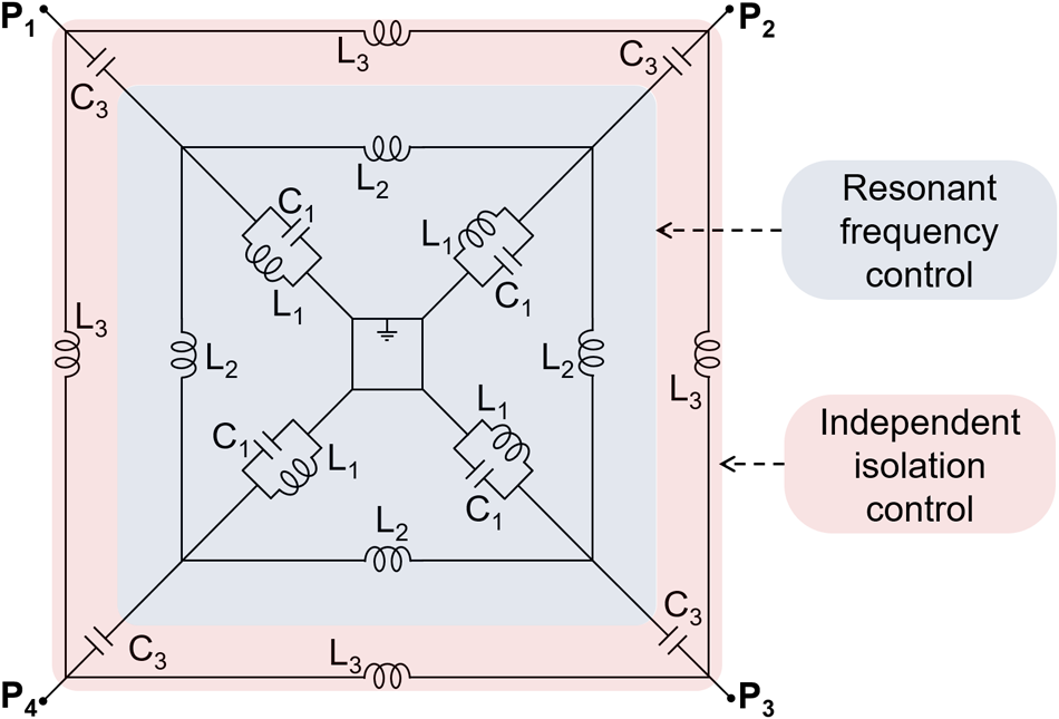
The equivalent circuit of the modified crossover circuit is shown in Fig. 4. Compared to the equivalent circuit shown in Fig. 2(c), a series capacitor ( $C_{3}$) is attached to each port. Also, each two adjacent ports are connected with each other by an inductor (
 $L_{3}$). These added elements provide a more degree of freedom to the crossover circuit to achieve a perfect isolation response between its channels, as discussed.
The equivalent circuit of the presented modified crossover, with designed and independent isolation control.

Figure 4 Long description
The diagram shows a modified crossover circuit with four ports labeled P subscript 1, P subscript 2, P subscript 3 and P subscript 4. Each port is connected to a series capacitor labeled C subscript 3. Between each pair of adjacent ports, there is an inductor labeled L subscript 3. Inside the circuit, there are additional inductors labeled L subscript 1 and L subscript 2 and capacitors labeled C subscript 1 and C subscript 2, arranged in a symmetrical pattern. The circuit is divided into two control regions: resonant frequency control and independent isolation control, as indicated by the labels. The resonant frequency control region is highlighted in blue, while the independent isolation control region is highlighted in red. The circuit is designed to achieve resonant frequency control and independent isolation between its channels.
Performing the even–odd mode analysis, the symmetrical form of the proposed equivalent circuit is shown in Fig. 5(a). The symmetry lines (AA’) and (BB’) are defined. For simplicity and to avoid redundancy, the even–odd mode analysis is performed without considering the external coupling behavior. Accordingly and by taking port 1 as the input port, the even-even, the even–odd/odd–even, and the odd–odd reduced circuits are shown in Fig. 5(b)–(d), respectively. The admittances seen from port 1 are expressed as follows
 \begin{equation}
{Y_{e e}}={\frac{j}{\omega}\left(\frac{C_3\left(\omega^2 L_1 C_1-1\right)}{L_1\left(C_1+C_3\right)-\frac{1}{\omega^2}}\right)}
\end{equation}
 \begin{equation}
{Y_{e o,o e}}={\frac{j}{\omega}\left(\frac{C_3\left(\omega^2 C_1-\frac{1}{L_1}-\frac{2}{L_2}\right)}{C_1+C_3-\frac{1}{\omega^2}\left(\frac{1}{L_1}+\frac{2}{L_2}\right)}-\frac{2}{L_3}\right)}
\end{equation}
 \begin{equation}
{Y_{o o}}={\frac{j}{\omega}\left(\frac{C_3\left(\omega^2 C_1-\frac{1}{L_1}-\frac{4}{L_2}\right)}{C_1+C_3-\frac{1}{\omega^2}\left(\frac{1}{L_1}+\frac{4}{L_2}\right)}-\frac{4}{L_3}\right)}
\end{equation}
For the presented modified crossover. (a) The equivalent circuit defining the symmetry lines  $AA'$ and
 $BB'$. (b) Even-even mode circuit. (c) Even–odd/odd–even mode circuit. (d) Odd–odd mode circuit.

Figure 5 Long description
The image consists of four sub-images labeled (a), (b), (c) and (d). Image (a) shows the equivalent circuit defining symmetry lines AA' and BB'. The circuit includes capacitors labeled C subscript 1 and C subscript 3 and inductors labeled L subscript 1 and L subscript 2. The circuit is symmetrical with components connected between ports P subscript 1, P subscript 2, P subscript 3 and P subscript 4. Inductors L subscript 2 are divided into L subscript 2 divided by 2 and inductors L subscript 1 are divided into L subscript 1 divided by 2. Image (b) shows the even-even mode circuit with port P subscript 1 connected to capacitor C subscript 3 and inductor L subscript 1 divided by 2. Image (c) shows the even-odd / odd-even mode circuit with port P subscript 1 connected to capacitor C subscript 1 and inductor L subscript 2 divided by 2. Image (d) shows the odd-odd mode circuit with port P subscript 1 connected to capacitor C subscript 3 and inductor L subscript 1 divided by 4. Each mode circuit is simplified to show specific connections and component values.
The isolation between the channels is controlled by the inductance ( $L_{3}$). The optimum isolation is obtained at the value of (
 $L_{3}$) where the conditions (11) and (13) are satisfied simultaneously. As shown in Fig. 6(a) and (b), the optimum isolation, at the resonant frequency of 8.7 GHz, is achieved at (
 $L_{3}$) of 27.3 nH. Also, Fig. 6(b) shows that the isolation between channels is independently-tuned through the inductance (
 $L_{3}$). The variation of the inductance (
 $L_{3}$) has no effect on the resonant frequency of the presented crossover circuit, as shown in Fig. 6(c). Moreover, Fig. 6(d) shows that the conditions (11) and (13) are achieved at the resonant frequency of 8.7 GHz at optimized values of
 $L_{1}$,
 $L_{2}$,
 $L_{3}$,
 $C_{1}$ and
 $C_{3}$ of 14.562 nH, 12.63 nH, 27.3 nH, 0.04 pF and 0.036 pF, respectively.
Controlling the isolation between the channels of the presented modified crossover circuit through the inductance ( $L_{3}$) at a resonant frequency of 8.7 GHz. (a) Defining the crossover’s optimum isolation point. (b) The simulated S-parameters of channel 1. (c) The effect of the inductance (
 $L_{3}$) on the resonant frequency. (d) Defining the conditions (11) and (13) at the resonant frequency with (
 $L_{3}$) of 27.3 nH. (All are simulated at
 $L_{1}$,
 $L_{2}$,
 $C_{1}$ and
 $C_{3}$ of 14.562 nH, 12.63 nH, 0.04 pF and 0.036 pF, respectively).

Figure 6 Long description
Panel (a) shows a line graph with the x-axis labeled Inductance L subscript 3 (nH) ranging from 17 to 37. The y-axis represents the isolation metric Gamma subscript e, with tick values visible. The graph compares Gamma subscript e equals 0 and Gamma subscript e equals plus 1, indicating optimum isolation at 27.3 nanohenry. Panel (b) displays a line graph with the x-axis labeled Frequency (GHz) from 7.7 to 9.7 and the y-axis labeled S-parameters of Ch. 1 (dB) from 0 to minus 60. Curves for S subscript 11 and S subscript 31 are shown, with resonance dips shifting across inductance values 35.3, 31.3, 27.3, 23.3 and 19.3 nanohenry. Panel (c) presents a line graph with the x-axis labeled Inductance L subscript 3 (nH) from 17 to 37 and the y-axis labeled Resonant frequency (GHz) from 8.5 to 9.5. Three series for C subscript 1 values of 0.03, 0.04 and 0.05 picofarad are plotted, showing resonant frequency stability across inductance. Panel (d) features a line graph with the x-axis labeled Frequency (GHz) from 7.7 to 9.7. The y-axis represents the isolation metric Gamma subscript e, with tick values visible. The graph highlights operating frequency at 8.7 gigahertz, comparing Gamma subscript e equals 0 and Gamma subscript e equals plus 1. Isolation increases with inductance, while S-parameters shift with frequency and inductance values, affecting resonance and transmission paths.
Realization
The modified crossover circuit, shown in Fig. 4, is implemented using the SIW technology, as it can handle high input power levels. The coupling diagram of the proposed SIW crossover is shown in Fig. 7(a). It consists of four LC tanks, each of which is coupled to a port. The external coupling of the ports is expressed by the external coupling coefficient ( $K_{e}$). The geometrical configuration of the proposed SIW crossover, generated using ANSYS HFSS [23], is shown in Fig. 7(b). Two stacked substrates are deployed in the structure. The main substrate is positioned on top of the secondary one. Both substrates act as one evanescent mode circular cavity, which is created by loading the conventional circular cavity with capacitive posts [Reference Liu, Katehi, Chappell and Peroulis24]. The main substrate holds four semicircular posts. Each semicircular post is loaded with a capacitive load in the secondary substrate, defined by the capacitive area (
 $A_{cap}$) as will be shown later. Four input/output ports are positioned with the same orientation as the posts. The ports are represented with grounded coplanar waveguide (G-CPW) feeding transmission lines, with a two-sided arc-shaped structure [Reference Hagag and Peroulis25] used to control the external coupling, which defines the crossover’s bandwidth. Figure 7(c) shows a comparison between a cross-sectional view of the proposed SIW crossover and its equivalent circuit shown in Fig. 4, representing the realization of the equivalent lumped elements (
 $L_{1}$,
 $L_{2}$,
 $L_{3}$,
 $C_{1}$ and
 $C_{3}$). The inductance (
 $L_{1}$) is represented by the inductive path formed by the semicircular posts and their connection to the cavity walls through the ground plane, while the capacitance (
 $C_{1}$) is embedded in the secondary substrate between the posts and the grounded middle layer. In other words, (
 $L_1$) and (
 $C_1$) are connected to the ground through the cavity walls and the middle metal layer, respectively. As the cavity walls and the middle metal layer are grounded and connected together, (
 $L_1$) and (
 $C_1$) are connected in parallel. Also, the inductance (
 $L_{2}$) is represented by the metalized connection between each two adjacent posts through the ground. This models the mutual inductive interaction through the ground, not direct port-to-port coupling. Moreover, the capacitances (
 $C_{3}$) are expressed by the slots in the cavity’s ceiling, while the conductive path between each two adjacent slots defines the inductance (
 $L_{3}$). A 2D view of the conductive layers of the presented SIW crossover is shown in Fig. 8(a)–(c), with related dimensions in mm.
For the presented SIW cavity crossover. (a) A coupling diagram. (b) A 3D geometrical view. (c) A comparison between a 3D cross-sectional view (not to scale) and its equivalent circuit. (The 3D images are generated using ANSYS HFSS [23], Version 2023.R1, https://www.ansys.com/products/electronics/ansys-hfss).

Figure 7 Long description
The image A shows a coupling diagram for an SIW cavity crossover. It includes four ports labeled P1, P2, P3 and P4, arranged in a circular configuration. Two channels are indicated, Channel 1 in black and Channel 2 in red, with arrows showing the direction of coupling between the ports. The external coupling coefficient is labeled as K subscript e. The image B presents a 3D geometrical view of the SIW crossover. The main substrate is positioned on top of the secondary substrate, with semicircular posts and slots visible on the main substrate. Four ports, labeled Port 1, Port 2, Port 3 and Port 4, are positioned around the structure. Cavity vias are shown connecting the substrates. The image C compares a 3D cross-sectional view with its equivalent circuit. The cross-sectional view displays the semicircular posts and cavity vias, with inductance and capacitance labeled as L subscript 1, L subscript 2, C subscript 1 and C subscript 3. The equivalent circuit diagram shows the arrangement of lumped elements, including inductors and capacitors, connected between ports P subscript 1, P subscript 2, P subscript 3 and P subscript 4. The inductance L subscript 1 is represented by the semicircular posts, while the capacitance C subscript 1 is embedded in the secondary substrate. The inductance L subscript 2 is shown as a metalized connection between adjacent posts and the capacitance C subscript 3 is expressed by slots in the cavity ceiling.
For the presented SIW cavity crossover, a two-dimensional view of the conductive layers. (a) Top layer. (b) Middle layer. (c) Bottom layer. (All units are in mm). The paths of the channels through the excited modes. (d) Channel 1 across mode 1. (e) Channel 2 across mode 2.

Figure 8 Long description
The diagram consists of multiple sub-images illustrating the SIW cavity crossover. In the first sub-image, labeled (a), there is a circular arrangement with four ports labeled Port 1, Port 2, Port 3 and Port 4. Metal vias are represented by blue circles and the metal areas are shaded. The second sub-image, labeled (b), shows a detailed view of the middle layer with dimensions marked in millimeters, including distances such as 2.8, 2.2 and 0.8. The third sub-image, labeled (c), illustrates the bottom layer with capacitive areas marked as 0.59 and 0.25 and the capacitive area labeled as A subscript cap. The fourth sub-image, labeled (d), presents a top view of Channel 1 with a circular pattern of metal vias and a side view showing the main substrate and secondary substrate. The fifth sub-image, labeled (e), shows Channel 2 with a similar arrangement and side view. Both channels display a color gradient indicating the intensity of the electric field, with a scale from min to max. The top views highlight the distribution of the electric field, while the side views show the structural arrangement of the substrates and channels. The diagram provides a comprehensive view of the SIW cavity crossover, illustrating the paths of the channels through the excited modes and the interaction between the substrates and metal vias.
By loading the SIW cavity with four capacitive posts, two orthogonal evanescent modes are excited at the same resonant frequency. The loaded capacitances ( $C_{1}$) exist in the secondary substrate only. As a result, and for these evanescent modes, all the electric fields are located only in the loaded capacitances (
 $C_{1}$). Moreover, most of the magnetic fields of these evanescent modes exist in the main substrate, where the majority of the inductance of the modes exists. The distributions of the fields of the two excited modes are shown in Fig. 8(d) and (e), for modes 1 and 2, respectively. As seen, the magnetic field of each mode rotates around a pair of semicircular posts in the main substrate. As the modes are orthogonal to each other, two isolated channels are created. As shown in Fig. 8(d), the magnetic field of mode 1 rotates around the horizontal pair of posts, creating channel 1. Moreover, the electric field exists in the secondary substrates between the horizontal posts in the bottom metal layer and the middle metal layer. Conversely, Fig. 8(e) shows the magnetic field of mode 2. It rotates around the vertical pair of posts, defining channel 2, while the electric field exists only on the vertical posts.
 \begin{equation}
{C_{1}}={\frac{\epsilon A_{cap}}{d}}
\end{equation}
A 3D cross-sectional view, generated using ANSYS HFSS [23], of the presented SIW crossover is shown in the inset of Fig. 9(a), showing one semicircular post. The post-loaded capacitance ( $C_{1}$) is defined by the area (
 $A_{cap}$) in the bottom conductive layer and the grounded middle one, where the cavity’s electric field is trapped in between. Using (17), the resonant frequencies of the modes are tuned by controlling the related loading capacitances, through adjusting the areas (
 $A_{cap}$), where (
 $\epsilon$) and (
 $d$) are the relative permittivity and the thickness of the secondary substrate, respectively. It is worth mentioning that (17) is based on a parallel-plate approximation and is valid under the assumption of a uniform electric field distribution between the area (
 $A_{cap}$) and the grounded layer. In other words, it is accurate when the distance (
 $d$) is small compared to the lateral dimensions of the capacitive area (
 $A_{cap}$), and without taking the fringing field into account. As shown in Fig. 9(a), the resonant frequency falls down with the rising value of the capacitance (
 $C_{1}$). To operate at a resonant frequency of 8.7 GHz, and using a 8 mil TC350 substrate with a relative permittivity of 3.5, the capacitive areas (
 $A_{cap}$) are designed to be approximately 1.3
 $\times$0.59
 $mm^2$, which yield capacitances (
 $C_{1}$) values of approximately 0.0467 pF, consistent with the equivalent circuit value and the simulated design shown in Fig. 3. As shown in Fig. 9(b), the variation of the resonant frequency of the proposed crossover cavity is studied with the radii of the cavity itself and its posts. As seen, increasing the radius of the proposed SIW cavity or the radii of the posts lowers the resonant frequency of the proposed crossover. Furthermore, the resonant frequency of the proposed power divider SIW-cavity decreases with the increasing distance between each two opposite posts, as shown in Fig. 9(c).
The tuning of the resonant frequency of the presented SIW cavity crossover through (a) the post-loaded capacitance ( $C_{1}$), simulated at
 $K_{e}$ of 0.091. (The 3D image is generated using ANSYS HFSS[23], Version 2023.R1, https://www.ansys.com/products/electronics/ansys-hfss). (b) the cavity and the post radii, simulated at post radius of 1.1 mm and cavity radius of 6 mm, respectively. (c) the distance (
 $x$) between each opposite post, simulated at cavity and post radii of 6 and 1.1 mm, respectively. (d) The tuning of the isolation between channels with the inductive distance (
 $d$) between the capacitive slots.

Figure 9 Long description
The tuning of the resonant frequency of the presented SIW cavity crossover through (a) the post-loaded capacitance (C1), simulated at Ke of 0.091. (b) the cavity and the post radii. (c) the distance (x) between each opposite posts. (d) The tuning of the isolation between channels with the inductive distance (d) between the capacitive slots. The image A showing a line graph with the y-axis labeled Resonant frequency (GHz) and the x-axis labeled Post-loaded capacitance (C1) pF. The x-axis runs from 0 to 2 in increments of 0.4. The y-axis runs from 3 to 11 in increments of 2. A legend lists Mode 1 and Mode 2. Mode 1 is a red curve with circular markers decreasing from about 10.5 at 0 to about 3.6 at 2. Mode 2 is a black curve near 10.8 to 11.0 across the range, with a slight dip around 1.2 to 1.6 and ending near 10.8 to 10.9 at 2. An inset schematic shows a cavity cross-section with labels Ke, W, E and Acap. The image B showing a line graph with the left y-axis labeled Resonant frequency (GHz) and the x-axis labeled Cavity radius (mm). The x-axis runs from 7.6 to 8.2 with ticks at 7.6, 7.8, 8.0 and 8.2. The left y-axis runs from 8.2 to 10.0 with ticks at 8.2, 8.6, 9.0, 9.4, 9.8 and 10.0. A right y-axis is labeled Post radius (mm) and shows values from 1.0 to 1.6. Two lines are plotted: a red line decreases from about 9.6 at 7.6 to about 8.2 at 8.2; a blue line decreases from about 9.0 at 7.6 to about 8.2 at 8.2. A small cross marker appears near cavity radius about 7.8 and resonant frequency about 9.0. The image C showing a line graph with the y-axis labeled Resonant frequency (GHz) and the x-axis labeled Distance between posts x (mm). The x-axis runs from 2.6 to 3.2 with ticks at 2.6, 2.8, 3.0 and 3.2. The y-axis runs from 8.9 to 9.2 with ticks at 8.9, 9.0, 9.1 and 9.2. A red line decreases from about 9.2 at 2.6 to about 8.9 at 3.2. An inset shows a circular arrangement of dots with a central cross and arrows labeled x. The image D showing a line graph with the y-axis labeled S-parameters (dB) and the x-axis labeled Frequency (GHz). The x-axis runs from 7.7 to 9.7 with ticks at 7.7, 8.2, 8.7, 9.2 and 9.7. The y-axis runs from 0 to minus 100 with ticks at 0, minus 20, minus 40, minus 60, minus 80 and minus 100. Curves labeled S11 and S31 are near the top region around 0 to minus 20, with a dip in S11 around 8.7 to 8.9. Multiple S21 curves are shown for d in mm with legend entries d equals 0.4, d equals 0.5, d equals 0.75, d equals 0.85 and d equals 1.0. The S21 curves form notches between about 8.4 and 9.0, with minima reaching roughly between minus 60 and minus 90 depending on the curve. An inset shows a circular dot pattern with a highlighted segment and a label d.
The isolation between channels comes from the orthogonality of the magnetic field distribution of the excited modes and the capacitive slots in the upper metalized layer of the main substrate. To obtain the isolation level due to the field orthogonality only, the proposed SIW cavity is simulated without the four capacitive slots and a 31 dB isolation level is obtained, as shown in Fig. 9(d). Afterward, the capacitive slots are added, and the isolation between the channels is tuned by changing the conductive path between each two adjacent capacitive slots. As shown in Fig. 9(d), properly choosing the distance ( $d$), maximal isolation is designed at the resonant frequency of the excited modes.
As shown in the inset of Fig. 9(a), a two-sided arc-shaped structure is used to externally couple the SIW cavity. Using the one-port model, the behavior of the external coupling coefficient ( $K_{e}$) is studied in Fig. 10. The physical parameters that control (
 $K_{e}$) are the feeding-arc angle (
 $\theta$), the feeding-arc width (
 $W$), and the distance (
 $d_{2}$) of the feeding-arc from the center of the cavity. As shown in Fig. 10(a), increasing (
 $\theta$) or (
 $W$), maximize (
 $K_{e}$). Moreover, moving the feeding-arc far from the center of the cavity decreases (
 $K_{e}$), as shown in Fig. 10(b). This comes to the fact that the magnetic field intensities of the excited modes increase toward the center of the cavity, where they reach their maximum values, as shown in Fig. 8(d) and (e), for modes 1 and 2, respectively. Furthermore, the coupling matrix of the proposed one-pole cavity crossover is expressed as follows
 \begin{equation}
\mathbf{M} =
\begin{bmatrix}
0 & M_{01} & 0 \\
M_{01} & 0 & M_{13} \\
0 & M_{13} & 0
\end{bmatrix}
\end{equation}
where the coupling coefficient ( $M_{01}$) represents the coupling between the source and crossover resonator, and (
 $M_{13}$) represents the coupling between the crossover resonator and load. The coupling coefficients are given by (19)
The external coupling behavior of the presented SIW cavity crossover against (a) the feeding-arc angle ( $\theta$), at different values of the feeding-arc width (
 $W$). (b) The distance between the center of the cavity and the feeding arc (
 $d_{2}$). (All are simulated at radii of 6 and 1.1 mm for the cavity and the posts, respectively).

Figure 10 Long description
The image A showing a line graph labeled (a). The x-axis label is Feeding-arc angle theta (degree), with tick labels 15, 25, 35, 45, 55, 65. The y-axis label is External coupling coefficient K subscript e, with tick labels 0.02, 0.03, 0.04, 0.05, 0.06, 0.07. A legend lists three series: W equals 0.1 millimeter, W equals 0.3 millimeter, W equals 0.5 millimeter. The plotted points shown on the lines are: W equals 0.1 millimeter: (15, 0.02), (25, 0.02), (35, 0.03), (45, 0.04), (55, 0.06), (65, 0.07). W equals 0.3 millimeter: (15, 0.04), (25, 0.04), (35, 0.04), (45, 0.05), (55, 0.06), (65, 0.07). W equals 0.5 millimeter: (15, 0.05), (25, 0.05), (35, 0.05), (45, 0.06), (55, 0.07), (65, 0.08). An inset diagram shows a circular shape with two arc segments and labels theta and W. The image B showing a line graph labeled (b). The x-axis label is Center-to-arc distance d subscript 2 (millimeter), with tick labels 4.9, 5.2, 5.5, 5.8. The y-axis label is External coupling coefficient K subscript e, with tick labels 0.12, 0.13, 0.14, 0.15. The plotted line passes through the following points: (4.9, 0.15), (5.2, 0.14), (5.5, 0.13), (5.8, 0.12). An inset diagram shows a circular dotted outline with a horizontal arrow labeled d subscript*2.
 \begin{equation}
{M_{01}=M_{13}=\frac{K_{e}}{\sqrt{\Delta}}}
\end{equation}
where  $\Delta$ is the fractional bandwidth of the resonator. Accordingly, coupling coefficients of 0.019 are obtained for the proposed crossover cavity, at a fractional bandwidth of 4.57.
Figure 11 demonstrates the capability to systematically synthesize higher-order transfer functions using the reported one-pole crossover cavity. This is achieved by cascading more filtering resonators in the path of each channel. As shown in the coupling diagram in Fig. 11(a), the higher-order crossover will have filtering order of n=1+m, where (m) is the number of added resonators in the path of each channel. For a second-order (n=2) crossover, a resonator (m=1) is added in the path of the signal of each channel. The geometrical configuration of the second-order crossover is shown in Fig. 11(b). The previously reported crossover cavity (cavity 1) is coupled to two additional SIW evanescent cavities (cavity 2 and 2’), one in the path of each channel (one cavity per pole per channel). As shown in Fig. 11(c). The added cavity is loaded with a single capacitive post, exciting one evanescent mode[Reference Liu, Katehi, Chappell and Peroulis24]. The equivalent circuit of the added SIW cavity resonator is represented by a parallel ( $LC$) tank, in which the capacitance (
 $C$) is represented by the capacitive post, while the cavity walls represent the inductance (
 $L$). The inset of Fig. 11(c) shows the distribution of the magnetic field for the excited evanescent mode. Moreover, by varying the capacitance plate radius (
 $R_{cap}$), the cavity’s resonant frequency can be adjusted, as shown in Fig. 11(c). Accordingly, the simulated resonant frequency of the additional cavity is tuned to coincide with the simulated resonant frequency of the proposed crossover cavity. For the second-order crossover shown in Fig. 11(b), the resonators of each channel are connected using a grounded CPW-TL. As the arc-shaped structures of each cavity added an additional phase delay, the total effective phase of the CPW-TL, two arc-shaped structures, and the two magnetic couplings at each cavity will give an effective -90
 $^\circ$ coupling (
 $k_{12}$) between resonators. The simulated scattering parameters of the second-order crossover architecture are shown in Fig. 11(d) and (e) for channels 1 and 2, respectively. It can be seen that both channels have simulated insertion losses of less than 1.9 dB and simulated reflection coefficients of more than 20 dB. Moreover, the proposed second-order crossover structure exhibits a high designed isolation level (
 $ \gt 50$ dB) between its channels, due to the added capacitive slots in the main crossover cavity (cavity 1), as previously explained.
The capability to systematically synthesize higher-order transfer functions in the proposed two-channel crossover by cascading more filtering cavities. (a) The coupling diagram. (b) A 3D geometrical view of a second-order crossover structure (n=2). (c) The variation of the simulated resonant frequency of the added filtering cavities, with the radius of their loaded capacitance plates. (Simulated at  $R_{cavity}$ and
 $D_{post}$ of 2.3 and 0.8 mm, respectively). The simulated S-parameters of the second-order (n=2) crossover. (d) Channel 1. (e) Channel 2. (This configuration has not been fabricated).

Figure 11 Long description
The image A shows a coupling diagram for a two-channel crossover system. It includes two channels labeled Ch. 1 and Ch. 2, each with resonators labeled P1, P2, P3 and P4. The filtering order is given as n equals 1 plus m, where m is the number of added resonators in each channel. The diagram illustrates connections between resonators with coupling coefficients k subscript e, k subscript m and k subscript 12. The image B presents a 3D geometrical view of a second-order crossover structure with ports labeled Port 1, Port 2, Port 3 and Port 4. The structure includes Cavity 1, Cavity 2 and Cavity 2 prime, with slots and arc-shaped structures. The diagram notes a total minus 90 degree effective coupling k subscript 12 and grounded CPW-TL. The image C shows a graph of resonant frequency in gigahertz versus R subscript cap in millimeters, with a linear decrease in frequency as the radius increases. An inset displays the cavity wall and capacitive post, with a magnetic field distribution. The image D illustrates simulated S-parameters for Channel 1, with frequency in gigahertz on the x-axis and S-parameters in decibels on the y-axis. The graph includes curves for S subscript 11, S subscript 21, S subscript 31, S subscript 41, S subscript 22, S subscript 32 and S subscript 42. The image E shows simulated S-parameters for Channel 2, with similar axes and curves for S subscript 22, S subscript 42, S subscript 32 and S subscript 44. Both channels demonstrate specific frequency responses and isolation levels.
Experimental results and discussion
The designed SIW cavity crossover is fabricated. Its top and bottom views are shown in Fig. 12(a) and (b), respectively. The crossover has a size of 12 $\times$12
 $mm^2$, without the feeding lines. The main substrate is realized utilizing a Rogers RO4003C substrate, with a thickness of 60 mil. In addition, the secondary substrate is realized using a 20 mil Rogers TC350 Plus substrate, which is used due to its high thermal conductivity.
For the presented one-pole SIW cavity crossover, a photograph of the fabricated prototype. (a) Top view. (b) Bottom view. A comparison between the simulated and the measured S-parameters. (c) Channel 1. (d) Channel 2. (Measured using a Keysight N5227B Vector Network Analyzer).

Figure 12 Long description
The image A showing a top-view photo of a square metal device with four coaxial connectors. Text labels near the connectors read Port 1, Port 2, Port 3 and Port 4. A small label below the photo reads (a). The image B showing a bottom-view photo of the same device with coaxial connectors. A small label below the photo reads (b). Channel 1 A line graph with the y-axis labeled S-parameters (decibel), ranging from 0 to minus 40. The x-axis is labeled Frequency (gigahertz), ranging from 7.7 to 9.7 with tick labels at 7.7, 8.2, 8.7, 9.2 and 9.7. A legend shows Simulated and Measured. Curve labels shown at the left are vertical-bar S11 vertical-bar, vertical-bar S33 vertical-bar, vertical-bar S31 vertical-bar, vertical-bar S21 vertical-bar and vertical-bar S41 vertical-bar. Multiple simulated and measured curves are plotted, including a deep notch near about 8.7 gigahertz reaching close to minus 40 decibel and other curves varying between about 0 and below minus 30 decibel across the frequency range. Channel 2 A line graph with the y-axis labeled S-parameters (decibel), ranging from 0 to minus 60. The x-axis is labeled Frequency (gigahertz), ranging from 7.7 to 9.7 with tick labels at 7.7, 8.2, 8.7, 9.2 and 9.7. A legend shows Simulated and Measured. Curve labels shown at the left are vertical-bar S22 vertical-bar, vertical-bar S42 vertical-bar, vertical-bar S32 vertical-bar and vertical-bar S12 vertical-bar. Multiple simulated and measured curves are plotted, including a deep notch near about 8.7 gigahertz reaching close to minus 60 decibel and other curves varying between about 0 and below minus 40 decibel across the frequency range.
A comparison between the simulated and measured S-parameters of the realized one-pole SIW cavity crossover is shown in Fig. 12(c) and (d), for channels 1 and 2, respectively. For the two channels and at a resonant frequency of 8.7 GHz, the measured return losses are higher than 20 dB. Additionally, a measured 1.7 dB insertion loss is achieved. It is worth mentioning that the proposed crossover cavity is simulated with an ideal copper conductivity of (5.8 $\times10^7$ S/m), yielding a simulated insertion loss of 1.38 dB. Simulating the crossover circuit using a lower copper conductivity of (1
 $\times10^7$ S/m), a higher simulated insertion loss of 1.7 dB is obtained. Accordingly, an extra insertion loss of 0.32 dB stems only from the conductor loss in the fabrication process. Also, the 3dB and 10dB roll-off bandwidths are measured to be 397.6 MHz and 1236 MHz, respectively. Moreover, a high isolation level of 64 dB is measured. A wide isolation bandwidth of 739 MHz is achieved at 50 dB, which can accommodate a wider passband operation, which can be achieved by cascading more cavities in each channel.
The setup shown in Fig. 13(a) is used to investigate the power handling capability of the realized SIW cavity crossover. Channel 1 is experimented by applying an amplified signal through port 1, while ports 2 and 4 are attached to 25 W matched loads. Also, port 3 is connected to a signal analyzer through a 30 dB directional coupler for protection. The output power level is observed using the signal analyzer, and the insertion loss of the presented crossover is calculated as shown in Fig. 13(b). It can be seen that the realized SIW cavity crossover handles a high-power level up to 44.7 dBm (29.5 W). Beyond this input power level, the crossover fails due to an air breakdown in the gap between the ground and the metalized post facing the input port (port 1), as shown in Fig. 13(b). As shown in Fig. 13(c) and at an input power of 20 W, a thermal-map image of the presented crossover is captured using a Fluke-Ti105 infrared camera. The measured heat map shows a maximum temperature of 31 $^\circ$C at the center of the cavity, as the magnetic field strength of the excited mode (mode 1) is maximum in the cavity’s center, coinciding with Fig. 8(d). It is worth mentioning that the output port (port 3) seems to be relatively colder than the input one (post 1). This returns to the increased value of the insertion loss of the proposed crossover, as the thermal image is captured at a high relative input power (43 dBm), which is close to the failure threshold (44.7 dBm).
The power handling capability measurement of the presented SIW cavity crossover. (a) A block diagram of the setup used. (b) The Measurement result. (c) A measured thermal map at an input power of 20W, using Fluke-Ti105 infrared camera.

Figure 13 Long description
The image consists of three parts. The first part, labeled as (a), is a block diagram illustrating the setup used for measuring the power handling capability of the SIW cavity crossover. It includes a signal generator connected to a power amplifier, which feeds into port 1 of the device under test (DUT). Ports 2 and 4 are connected to 25 watt loads, while port 3 is linked to a signal analyzer through a 30 decibel coupler and a 20 decibel attenuator. The second part, labeled as (b), is a graph showing the insertion loss in decibels on the y-axis versus the input power in decibels-milliwatts on the x-axis. The graph indicates a failure point at 44.7 decibels-milliwatts, corresponding to 29.5 watts, due to an air breakdown. An inset image shows the physical location of the failure between the ground and the metalized post facing port 1. The third part, labeled as (c), is a thermal map captured at an input power of 20 watts using an infrared camera. The map displays temperature distribution with a maximum of 28.5 degrees Celsius at the center of the cavity. Ports 1, 2, 3 and 4 are marked on the thermal map, showing varying temperature levels across the crossover.
Table 1 shows a comparison between our realized works and the other state-of-the-art SIW cavity crossovers. Compared to the highest isolation level (36 dB) obtained by the state-of-the-art SIW filtering crossovers in [Reference Sun, Deng, Xue, Zhu and Xing11], the proposed first- and second-order crossovers achieve higher isolation levels of 64 dB and 50 dB, respectively. The proposed high-isolation between channels is obtained with comparable sizes, except for [Reference Lai, Yang, Chi and Ruimin14], which is not suitable for high-power applications due to the utilized low power handling varactor diodes. Although the crossover structure stated in [Reference Lili, Zhang, Liu, Xiaole, Jing and Fan12] operates in dual pass-bands, it has a low isolation level of 14.65 dB. Moreover, the operating frequencies of each channel in [Reference Zhou and Wu8, Reference Lai, Yang, Chi and Ruimin14] can be independently tuned; the isolation between these channels is less than 20 dB. Furthermore, our work is the only crossover to report high-power handling measurements. It handles up to 44.7 dBm (29.5 W) of input power, with a relatively low insertion loss, suitable for dealing with high-power RF applications.
Comparison with state-of-the-art SIW cavity crossovers

Table 1 Long description
The table compares SIW cavity crossover designs by center frequency in gigahertz, fractional bandwidth in percent, filter order, insertion loss in decibels, isolation in decibels, and normalized size in guided-wavelength squared units. Prior works span 5 to 20 gigahertz, with one design covering 1.88 to 2.81 gigahertz and another reporting two bands at 7.11 and 8.77 gigahertz. Fractional bandwidths range from 2.41 percent to about 7.21 percent, while filter order ranges from 2 to 5 in the referenced designs. Insertion loss for the references ranges from 1.33 to 3.29 decibels, and isolation ranges from 14.65 to 36 decibels, with the highest reference isolation reported at 36 decibels at 10.2 gigahertz. The smallest referenced size is 0.36 guided-wavelength squared for the 1.88 to 2.81 gigahertz design, while several others are around 6.3 to 6.5 guided-wavelength squared. The two entries labeled as this work are both at 8.7 gigahertz and report much higher isolation than the references: 64 decibels for the first-order design and 50 decibels for the second-order design. Their insertion losses are 1.7 and 1.9 decibels, with fractional bandwidths of 4.57 percent and 2.75 percent, and sizes of 0.42 and 2.17 guided-wavelength squared, respectively. One of the this-work results is simulation-only, and both this-work sizes are reported without feeding lines, so direct size comparisons to other rows may not be fully equivalent.
Notes: FBW: Fractional bandwidth, N: filtering order, IL: Insertion loss, Iso.: Isolation,  $\star \rightarrow$ Simulated results only (not fabricated),
 $\ddagger \rightarrow$ Without feeding lines.
Conclusion
A novel high-power SIW cavity crossover with a high isolation level is presented. It consists of a circular evanescent-mode cavity resonator with two pairs of semicircular posts crossed. Each post is connected to a loading capacitance ( $C_{1}$). The cavity excites two evanescent modes, with the distribution of their magnetic fields orthogonal to each other. At the same loading capacitance (
 $C_{1}$), the modes are excited at the same resonant frequency. Accordingly, two isolated channels are created. The proposed one-pole cavity has a size of (0.65
 $\lambda_{g}\times$0.65
 $\lambda_{g}$), including the feeding lines. Moreover, a measured insertion loss and isolation of 1.7 dB and 64 dB are obtained, respectively. Also, measurements showed that the crossover handles an input power level up to 44.7 dBm (29.5 Watts). Moreover, the scalability of the one-pole crossover cavity to higher-order transfer functions has been demonstrated in a simulated two-channel crossover configuration, with enhanced frequency response. The main contribution of this work is not merely the realization of another SIW crossover topology, but the demonstration of compact high-power crossover cavities with significantly enhanced channel isolation suitable for working in high-power RF applications.
Competing interests
The authors declare none.

Kareem H. El-Gendy received the B.Sc. degree, with a grade of excellent with honors, in electrical engineering from the Electrical Engineering Department, Military Technical College, Cairo, Egypt, in 2019. He was awarded the M.Sc. degree in electrical engineering in 2025 from Military Technical College, where he is currently a Research Assistant in electrical engineering with the Military Technical College. His research focus is on reconfigurable RF front-end components based on high- $Q$ cavities, tunable and switchable coupling networks, superconducting and cryogenic microwave circuits for advanced communication and quantum-enabled applications.

Mohammad Darwish received the B.Sc. (Hons.) and M.Sc. degrees in electrical engineering from the Military Technical College, Cairo, Egypt, in 2001 and 2008, respectively, and the Ph.D. degree in electrical engineering from the University of California, Davis, CA, USA, in 2013. Since then, he joined the Military Technical College, as an Assistant Professor, where he is currently the Head of the Radar Department. In 2019, he was a Visiting Scholar at the School of Electronic Engineering, Xidian University, Xi’an, China. His research interests include RF and microwave hybrid and integrated circuits, especially power amplifiers, antennas, and radars. His research also focuses on transceiver architectures and RF front-end performance enhancement for modern communication systems.

Mahmoud A. Abdalla was born in 1973. He received the B.Sc. degree, with a grade of excellent with honors, in electrical engineering from the Electrical Engineering Department, Military Technical College, Cairo, Egypt, in 1995. He was awarded the M.Sc. degree in electrical engineering from Military Technical College in 2000, and the Ph.D. degree from the Microwave and Communication group, School of Electrical Engineering, Manchester University, UK, in 2009. Since 1996, he has been with Military Technical College, where he is now a Professor, the Head of the Electromagnetic Waves/Microwave Group in the Electronic Engineering Department, and the Head of the Electronic Engineering Department and the Department Council Committee. Also, he has been a Visiting Professor in the Department of Computer and Electrical Engineering, University of Waterloo, Canada, since 2017. Prof. Abdalla has been a Senior Member of the IEEE since 2015.

Mohamed Fouad Hagag received the B.Sc. and M.Sc. degrees in electrical and computer engineering from Military Technical College (MTC) in 2007 and 2013, respectively, and the Ph.D. degree in electrical and computer engineering from Purdue University in 2018. From 2009 to 2014, he served as a Research and Teaching Assistant at MTC, where he worked on metamaterials, microwave and millimeter-wave components, miniaturized antennas, and radar absorbers. Between 2015 and 2018, he conducted research at Purdue University and the Birck Nanotechnology Center on reconfigurable RF front-end systems based on high-Q cavity resonators. He is currently an Associate Professor at MTC, focusing on superconducting quantum hardware, reconfigurable RF/microwave systems, time-varying circuits, and advanced microwave components for communication, sensing, and quantum technologies. Dr. Hagag has authored numerous publications and received awards at the IEEE Wireless and Microwave Technology Conference and the IEEE International Microwave Symposium.