1. INTRODUCTION
The development of high-power X-ray technologies is inspired by research in materials exposed to intense irradiation, using of X-ray sources for radiography in high-energy-density conditions experiments (Sharkov et al., Reference Sharkov, Hoffmann, Golubev and Zhao2016), industrial applications (sterilization and modification of materials, ecological problem solving, foodstuff treatment, etc.). The main research lines in designing pulsed X-ray sources concern the generation of high-voltage pulses (Filatov et al., Reference Filatov, Kotov, Mesyats and Sokovnin1989; Mesyats et al., Reference Mesyats, Korovin, Gunin, Gubanov, Stepchenko, Grishin, Landl and Alekseenko2003; Li et al., Reference Li, Liu, Xu, Chen, Chang, Wan and Wen2009) and electron beams (Ozur et al., Reference Ozur, Proskurovsky, Rotshtein and Markov2003; Cai et al., Reference Cai, Liu, Ju, Zhao and Qiu2014, Reference Cai, Liu, Ju, Zhao, Zhou and Wang2016; Kozyrev et al., Reference Kozyrev, Kozhevnikov, Vorobyov, Baksht, Burachenko, Koval and Tarasenko2015).
Repetitive pulsed sources of intense X rays (bremsstrahlung) require an increase in the lifetime of their converters, which convert the energy of a high-current electron beam to radiation (Danko et al., Reference Danko, Dolgachev and Ushakov2005). One of the ways to solve the problem is to use a massive anode instead of a thin anode target of thickness comparable with the electron path length (Berger & Seltzer, Reference Berger and Seltzer1970). The diode geometry with a massive anode can be coaxial and the central anode conductor can be a rod.
Cylindrical diodes with rod anodes have found wide application in relatively low-power X-ray sources for defectoscopy (Ivanov & Shchukin, Reference Ivanov, Shchukin and Dolgopolova1989) as well as in high-power pulsed X-ray sources for radiography in magnetohydrodynamic experiments (Mahaffey et al., Reference Mahaffey, Golden, Goldstein and Cooperstein1978; Cooperstein et al., Reference Cooperstein, Boller, Commisso, Hinshelwood, Mosher, Ottinger, Schumer, Stephanakis, Swanekamp, Weber and Young2001) and for production of high-energy-density plasma (Weber et al., Reference Weber, Apruzese, Mosher, Phipps, Schumer and Stephanakis2013). The characteristic radial size of an anode in such diodes is ~1 mm, the gap between the anode and the cathode is also ~1 mm, and the supply voltage pulse is no longer than 100 ns. The diode resistance is rather low, measuring several tens of Ohms, which allows efficient use of low-resistance high-power generators. However, the small radial size of the anode does not allow the use of the diodes in repetitive pulsed high-current sources, and the small interelectrode gap imposes limitations on the supply pulse duration.
By increasing the anode diameter an order of magnitude, one may expect successful operation of a rod-anode diode in repetitive pulsed mode. At a small ratio of cathode to anode radii r C/r A ~ 3, it is possible to provide a diode resistance of several tens of ohms, and if we preliminary fill the diode with plasma, it is possible to realize beam pinching by the self-magnetic field at a voltage of ~105 V. In the latter case, the diode is an efficient source of intense X rays. This paper studies the possibility of using a plasma-filled cylindrical diode with a rod anode in a repetitive pulsed X-ray source.
2. DIODE DESIGN AND EXPERIMENTAL ARRANGEMENT
The design of a plasma-filled diode with a rod anode is shown in Figure 1. The anode (1) of the diode is a tungsten rod of diameter 10 mm located at the end of the potential conductor of a vacuum transmission line. The cathode (2) is a stainless steel disc of thickness 1 mm with a hole of diameter 30 mm at its center. The anode rod passes through the center of the cathode hole, protruding beyond the cathode plane by a distance s.
Diode with rod anode: 1, anode; 2, cathode; 3, potential electrode of the plasma source; 4, bushing insulator of the plasma source; 5, output window; dI/dt, inductive sensor measuring the diode current derivative.

The potential electrode (3) of the plasma source is a stainless steel cylinder of inner diameter 56 mm. As a voltage of negative polarity is applied to the potential electrode (3) from a separate generator through bushing insulators (4), cathode spots are initiated at the sharp edge of the electrode (3) and an auxiliary vacuum discharge is ignited between this electrode and the cathode (2). The ion flow from the cathode flare moves toward the anode rod and fills the diode gap between the anode (1) and cathode (2) before applying a voltage pulse to the diode from the main generator. The potential electrode (3) also protects the bushing insulators (4) from contamination with sputtered anode material.
The X rays are extracted through a duralumin flange (5) of thickness 1 mm, which cuts off the radiation with a photon energy lower than 10 keV. At a photon energy of 20 keV, the radiation intensity through the flange decreases by about 60% and at 50 keV by 10%.
The plasma source is powered from an 8 nF capacitor charged to 80 kV. The discharge current amplitude in the plasma source is 6 kA; the half-period is 300 ns.
The diode is powered from a capacitor bank of equivalent capacitance C = 8 nF. The charge voltage of the bank is up to 300 kV. The capacitor bank is switched by a spark gap switch with a time delay t
d with respect to the instant of operation of the plasma source. The discharge circuit parameters are the following: inductance L ≈ 1000 nH and resistance R ≈ 2.8 Ω. The wave impedance of the discharge circuit is
 ${\rm \rho} = \sqrt {L/C} $
≈ 11 Ω. On discharging the capacitor bank onto a constant resistive load, the power peaks is realized at a load resistance R
d = 1.1ρ + 0.8R (Stygar et al., Reference Stygar, Cuneo, Headley, Ives, Leeper, Mazarakis, Olson, Porter, Wagoner and Woodworth2007). For the parameters of our discharge circuit, the optimum diode resistance on direct discharging of the capacitor bank is R
d ≈ 14 Ω. The estimated parameters of the output pulse at a load with a constant resistance of 14 Ω and capacitor bank charge voltage of 210 kV are the following: current amplitude 7.8 kA, voltage amplitude 110 kV, and peak power ~0.9 GW.
3. DIODE-OPERATING MODES
3.1. Experimental results
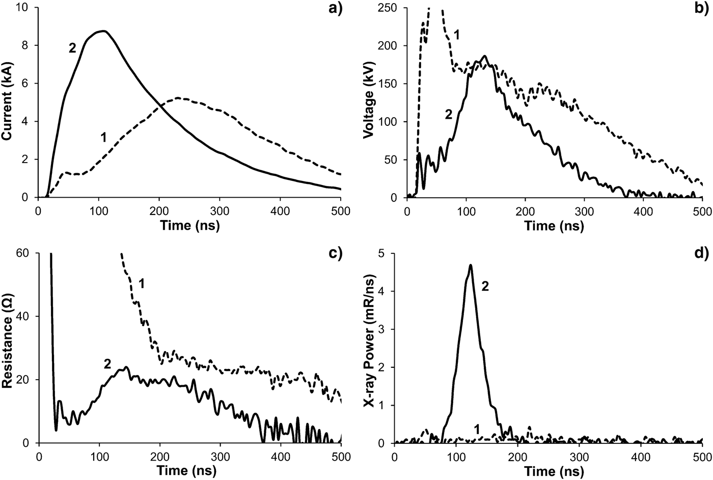
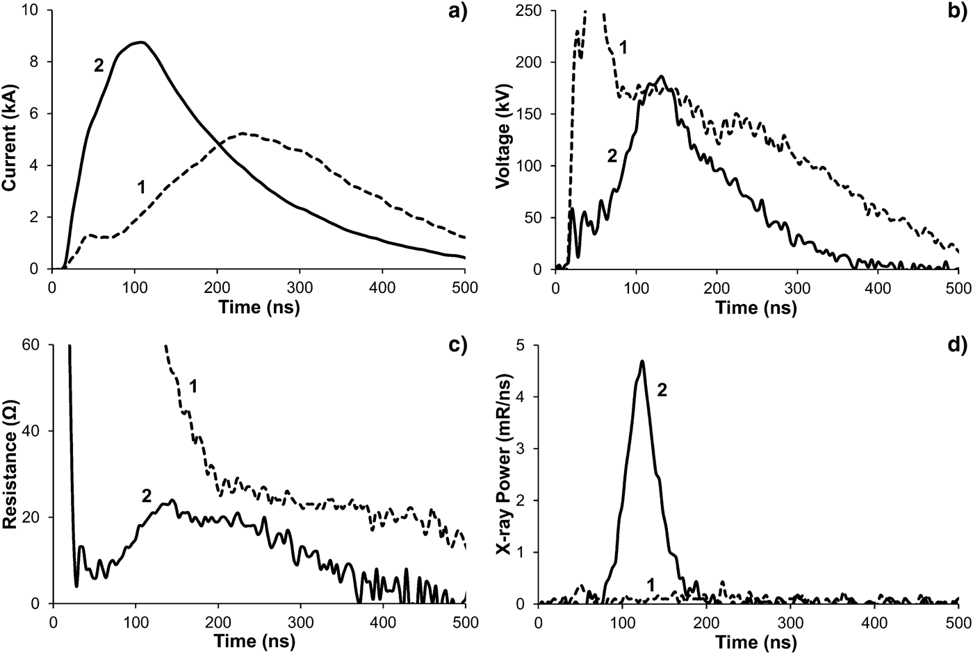
Figure 2 demonstrates the operating mode of the rod-anode diode at a capacitor bank charge voltage of 210 kV. The switching delay time t d for the capacitor bank with respect to the instant of operation of the plasma source is 0.2 and 3 µs. The rod anode protrudes beyond the cathode plane by s = 27 mm.
Oscillograms of the current (a), voltage (b), resistance (c), and X-ray power (d) for a switching delay time of 0.2 µs (curves 1) and 3 µs (curves 2).
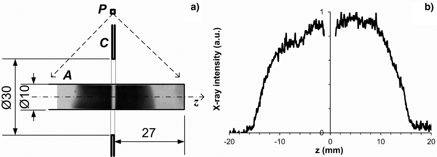
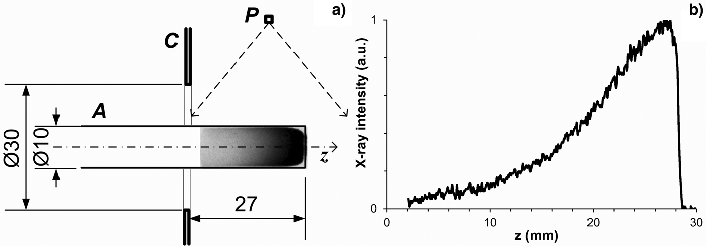
Figures 3 and 4 show X-ray images of the anode and radiation intensity along the anode axis at t d equal to 0.2 and 3 µs. The images were taken downstream of an Al filter 0.2 µs thick using a pinhole camera and Kodak Dental Intraoral D-speed film. The location of the camera is indicated as P in the figures.
X-ray image of the anode (a) and radiation intensity along the anode axis (b) at t d = 0.2 µs. A, anode; C, cathode; P, pinhole camera; z = 0, cathode plane.

X-ray image of the anode (a) and radiation intensity along the anode axis (b) at t d = 3 µs. A, anode; C, cathode; P, pinhole camera; z = 0, cathode plane.

With a small delay time (Fig. 2, curves 1), the influence of the plasma source is insignificant and the diode operates in the mode of space-charge-limited current. The magnetic field in the diode weakly affects the electron trajectories; the anode region of bremsstrahlung X rays is symmetric about the cathode plane (Fig. 3). The diode resistance reaches a quasi-steady level of ~25 Ω in 200 ns and is kept at this level for up to 500 ns. Thus, the interelectrode gap equal to 1 cm provides an energy extraction time from the capacitor bank of more than 500 ns, allowing the formation of a submicrosecond pulse. The peak power in the diode is 0.7 GW at the time point 220 ns with a diode current of 5.1 kA and voltage of 140 kV. The peak power is 30% lower than that during the operation onto a matched load with constant resistance. The X-ray power at a distance of 20 cm from the anode face is <0.2 × 10⁶ R/s.
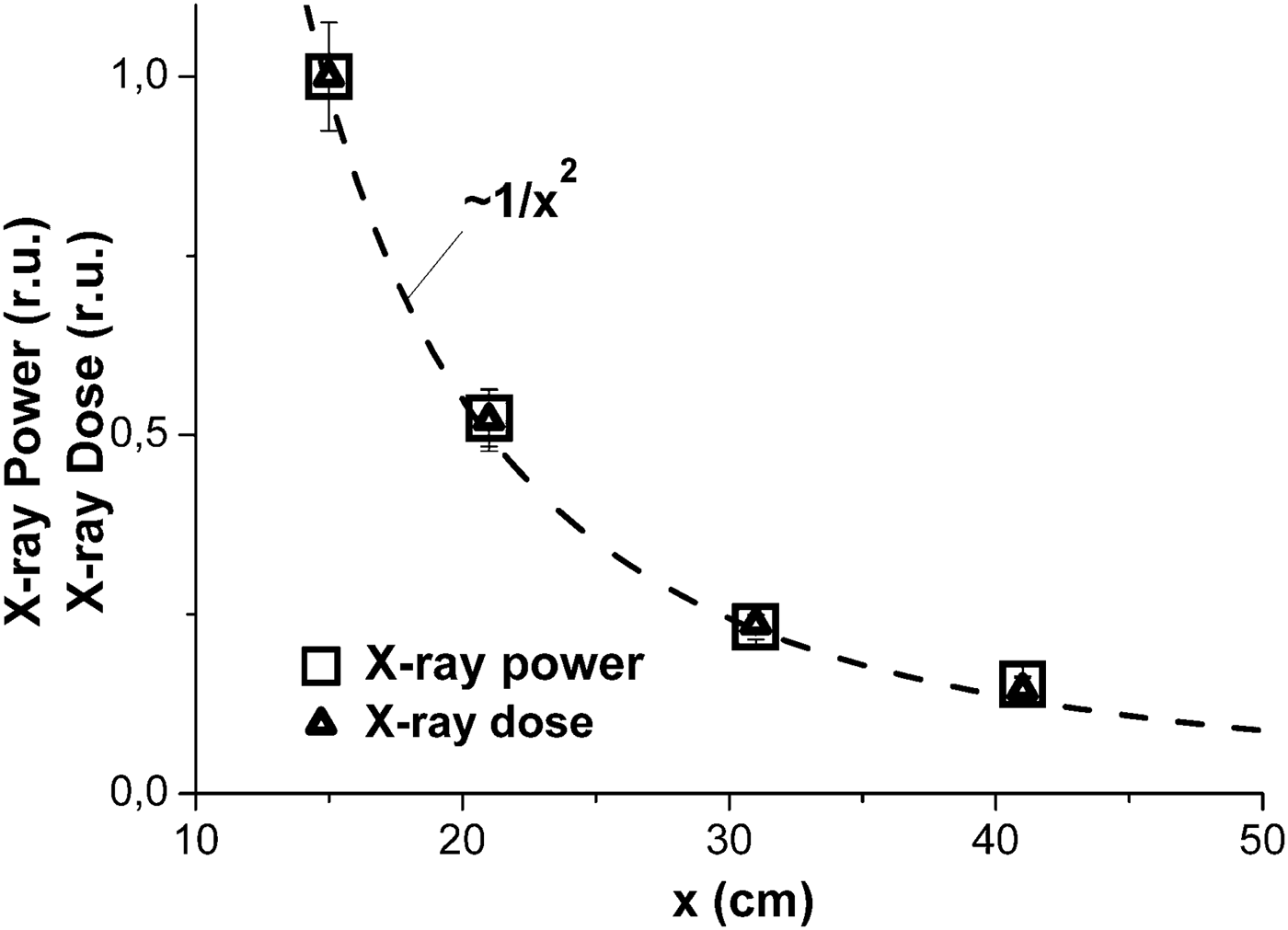
Increasing the delay time (Fig. 2, curves 2) increases the influence of preliminarily injected plasma on the diode parameters. The plasma assists faster formation of a homogeneous emission surface at the cathode and compensates the space charge of the electron beam. Upon applying a voltage pulse, the diode resistance decreases steeply to 6 Ω and is kept low within 50 ns. During this time, the diode voltage is about 50 kV and the diode current increases to 6 kA. Due to erosion (Ottinger et al., Reference Ottinger, Goldstein and Meger1984; Bolotov et al., Reference Bolotov, Kozyrev, Kolesnikov, Korolev, Rabotkin and Shemyakin1991) and/or current-carrying plasma acceleration by a force J × B (Weber et al., Reference Weber, Commisso, Hinshelwood, Mosher, Ottinger, Ponce, Schumer, Stephanakis, Strasburg, Swanekamp and Young2004), the plasma density in the diode gap decreases and the diode resistance increases with a rate of 0.25 Ω/ns. The resistance reaches a level of about 21 Ω, which is close to the vacuum diode resistance. At this time point, the diode current is 8.7 kA and the diode voltage is 180 kV. An energy of 160 J with a peak power of 1.5 GW is dissipated in the diode. The attained power is 1.5 times higher than the maximum power during the operation of the capacitor bank onto a matched load with constant resistance. According to the image in Figure 4, the electron beam is pinched to the anode edge with the formation of a high-power X-ray pulse. The peak of the X-ray power coincides in time with the peak of the diode power. At 20 cm away from the anode face, the peak power is 5 × 10⁶ R/s and the radiation dose per pulse is 0.22 R. The full-width at half-maximum (FWHM) of the radiation pulse is 40 ns. The peak power and the X-ray dose are inversely proportional to the squared distance to the radiation source (Fig. 5).
X-ray power and dose versus distance to the radiation source; normalized to values at x = 15 cm.

3.2. Modeling
By convention, there are three possible operating modes of a cylindrical diode (Mahaffey et al., Reference Mahaffey, Golden, Goldstein and Cooperstein1978). When the magnetic field effect in the diode is low, the current of the beam is limited by its space charge and is described by the Langmuir–Blodgett equation (Langmuir & Blodgett, Reference Langmuir and Blodgett1923):
 $$I_{{\rm SCL}} = I_0 {\rm \alpha} _1\displaystyle{{2\sqrt 2} \over 9}\displaystyle{{L_{{\rm eff}}} \over {r_{\rm A}k^2}}U_{\rm d}^{{\rm 3/2}}, $$
where I 0 = 17 kA; r A is the anode radius; k is the coefficient dependent on the ratio of cathode and anode radii r C/r A; U d is the diode voltage in CGS units. The coefficient α1 allows for ion emission from the anode. For the bipolar operation of the diode, α1 = 1.86 (Swanekamp et al., Reference Swanekamp, Commisso, Cooperstein, Ottinger and Schumer2000; Cooperstein et al., Reference Cooperstein, Boller, Commisso, Hinshelwood, Mosher, Ottinger, Schumer, Stephanakis, Swanekamp, Weber and Young2001). The effective diode length L eff is larger than the physical length of the cathode due to electron flow expansion toward the anode. For our diode, the effective length estimated from the X-ray image of the anode (Fig. 3) is L eff ≈ 30 mm. The coefficient k was calculated elsewhere (Langmuir & Blodgett, Reference Langmuir and Blodgett1923), and for simulation, it was proposed to use the approximation (Cooperstein et al., Reference Cooperstein, Boller, Commisso, Hinshelwood, Mosher, Ottinger, Schumer, Stephanakis, Swanekamp, Weber and Young2001):
 $$k = - z - 0.4z^2 - 0.0917z^3 - 0.0144z^4 - 0.0017z^5 - 0.0002z^6,$$
where
 $z = \ln (r_{\rm C}/r_{\rm A})$
. At r
C/r
A = 3, k ≈ 1.7.
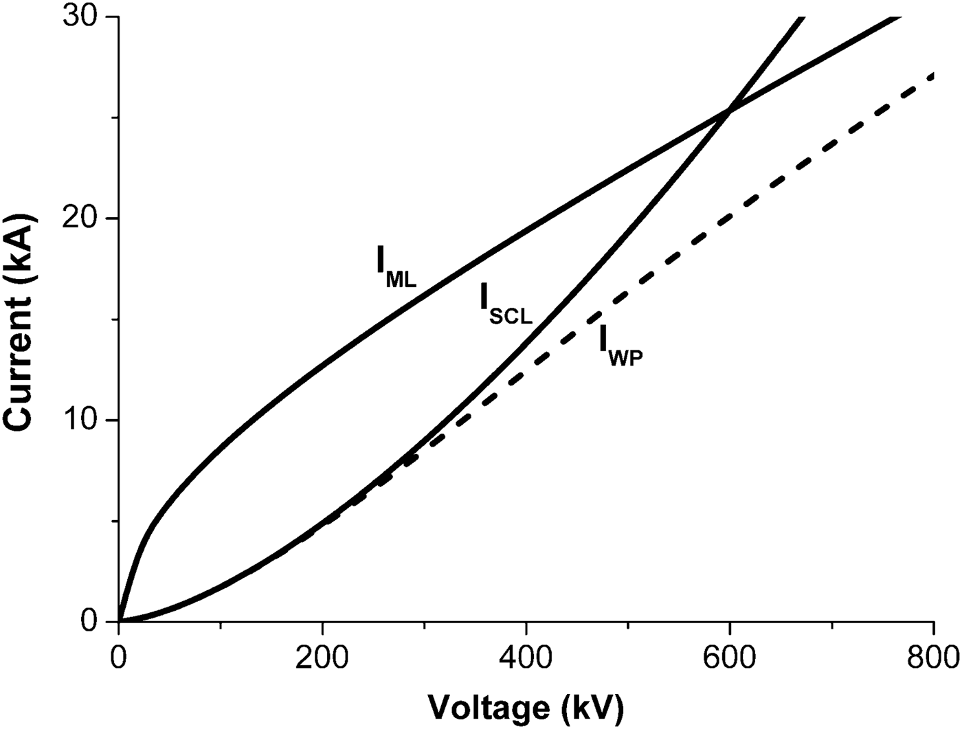
As the current is increased, the influence of the self-magnetic field grows such that the electron trajectories are curved, and in the limiting case, when the Larmor radius of electrons becomes comparable with the interelectrode gap, the diode passes to the mode of self-magnetic insulation. The critical current for self-magnetic insulation is expressed as (Mahaffey et al., Reference Mahaffey, Golden, Goldstein and Cooperstein1978):
 $$I_{{\rm ML}} = \displaystyle{{I_0} \over 2} {\rm \alpha} _2\displaystyle{{\sqrt {{\rm \gamma} ^2 - 1}} \over {\ln {\kern 1pt} (r_{\rm C}/r_{\rm A})}},$$
where γ is the relativistic factor. The coefficient α2 ≤ 2 depends on the ratio r C/r A and external current of the diode (Kirikov et al., Reference Kirikov, Belomyttsev, Ryzhov, Turchanovsky and Tarakanov2003). According to Cooperstein et al. (Reference Cooperstein, Boller, Commisso, Hinshelwood, Mosher, Ottinger, Schumer, Stephanakis, Swanekamp, Weber and Young2001), coefficient α2 is equal to ~1.7 at r C/r A = 3.
In the transition mode between (1) and (2), the electron beam is weakly pinched. The diode current is approximated by the dependence (Swanekamp et al., Reference Swanekamp, Commisso, Cooperstein, Ottinger and Schumer2000):
 $$\displaystyle{1 \over {I_{{\rm WP}}^{\rm 3}}} = \displaystyle{1 \over {I_{{\rm SCL}}^{\rm 3}}} + \displaystyle{1 \over {I_{{\rm ML}}^{\rm 3}}}. $$
According to experiments, to produce intense bremsstrahlung X rays, it is required that the electron beam be pinched at the end of the anode rod.
Figure 6 presents calculated currents dependances of voltage (1)–(3) for our diode geometry at r C/r A = 3. The dependences allow us to estimate the operating mode of the diode from the measured current and voltage. The self-magnetic field starts showing its effect only at a diode voltage above 300 kV. Strong pinching of the electron beam in the vacuum diode requires a voltage higher than 1000 kV. To provide the pinching mode and the generation of intense X rays at low voltages (100–200 kV) and fixed radial diode sizes, it is required to increase the current. An efficient way to increase the current is to compensate the space charge of the electron beam by preliminary filling the diode gap with plasma. The results of experiments confirm the possibility of electron beam pinching at a voltage of <200 kV in the plasma-filled cylindrical diode.
Electron current dependence of voltage in cylindrical vacuum diode. I SCL, current in space-charge-limited mode; I ML , critical current for self-magnetic insulation; I WP , current in weak pinching mode.

4. EFFECT OF PLASMA INJECTION TIME ON DIODE PARAMETERS
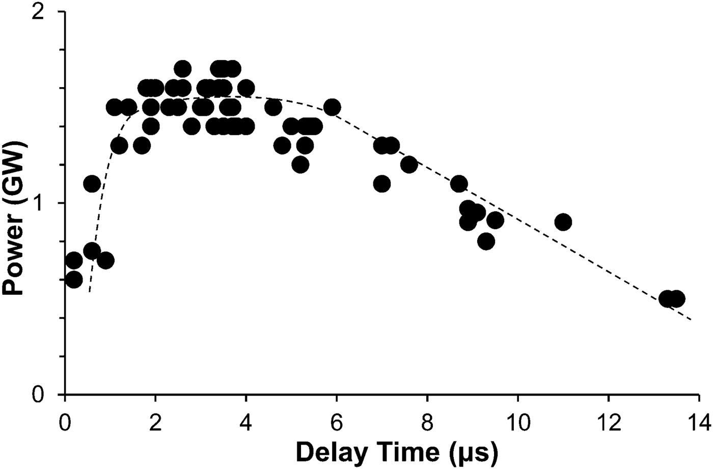
One of the possible ways of realizing a repetitive pulsed generator for X-ray and plasma sources is pulsed charging of a high-voltage capacitive store from a primary low-voltage store through a step-up transformer (Kovalchuk et al., Reference Kovalchuk, Kharlov, Vizir, Kumpyak, Zorin and Kiselev2010). In this circuit, the high-voltage capacitive store is switched by a spark gap switch in the self-breakdown mode. At a rate of voltage rise of several kilovolts per microsecond and voltage rise time to the instant of breakdown of 50–100 µs, the time jitter of self-breakdown can measure a few microseconds. Thus, the plasma source and the main generator can also be synchronized accurate to a few microseconds, and the diode parameters are bound to vary slightly in this range of delay times t d. Figure 7 demonstrates how the switching delay time of the capacitor bank with respect to the instant of operation of the plasma source influences the power attained in our diode. It is seen that the diode has a rather wide range of t d, measuring 2–5 µs, where the peak power of the beam is not below 1.2 GW at a charge voltage of the capacitor bank of 210 kV. In this range of t d, the radiation power 20 cm away from the anode face is about 2 × 10⁶ R/s and the radiation dose per pulse is ~0.11 R.
Diode power versus switching delay time at a capacitor bank charge voltage of 210 kV.

5. EFFECT OF ANODE LENGTH ON DIODE PARAMETERS
The effect of the rod anode length s on the parameters of the diode and X rays was studied at a capacitor bank charge voltage of 260 kV. The increase in the charge voltage from 210 to 260 kV allowed us to increase the peak power of the diode to 1.8 GW (10 kA, 180 kV). At a distance of 20 cm from the anode, X rays with a power of about 7 × 10⁶ R/s were detected. The radiation dose per pulse was ~0.4 R.
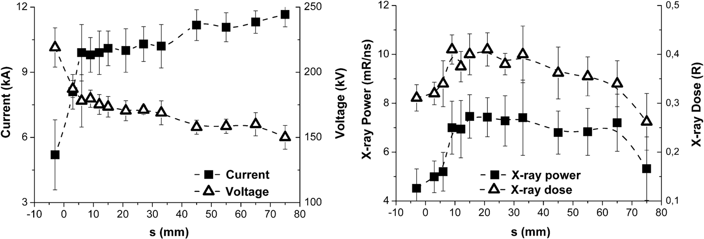
The research results are summarized in Figure 8. The length s = 0 corresponds to the position of the rod face in the cathode plane. The distance between the anode face and the X-ray sensor is 20 cm. For each value of s, no <10 shots at t d = 2–5 µs were realized, whereupon the average of a quantity and its standard deviation were calculated.
Diode current, voltage, X-ray power, and dose versus anode rod length.

Increasing the anode length to over 10 mm causes a sharp decrease in the diode impedance and an increase in the X-ray power. As the anode length is further increased to 65 mm, the diode resistance decreases gradually from 18 to 14 Ω. Any significant change in the X-ray power is not observed. The latter fact is important for the diode operating in repetitive pulsed mode because the decrease in the anode length due to electron beam ablation of the anode material will not affect the radiation power over a wide range of s.
6. CONCLUSION
Thus, we studied the plasma-filled cylindrical diode with a rod anode for use in repetitive pulsed intense X-ray sources. The plasma source based on cathode flare produced in a vacuum discharge allowed us to realize electron beam pinching at a voltage of <200 kV, anode diameter of 1 cm, and ratio of cathode and anode radii of 3. The massive anode resolves the problem of the converter lifetime.
The peak power in the diode is 1.8 GW at a current of 10 kA and voltage of 180 kV and exceeds the maximum power of the capacitor bank operating onto a matched load with constant resistance. The peak power and the X-ray dose are inversely proportional to the squared distance to the radiation source. The X-ray dose at 20 cm from the radiation source (downstream of a duralumin flange 1 mm thick) is 0.4 R per pulse with a peak power of 7 × 10⁶ R/s. The FWHM of the pulse is 40 ns.
The time range of preliminary plasma injection in the diode is wide, measuring 2–5 µs.
ACKNOWLEDGMENTS
The work was supported by the Russian Foundation for Basic Research (RFBR; Grant no. 15-08-00741-a).