Introduction
Filters are one of the most important components used in modern communication systems. There are many different methods for designing filters to suppress unwanted signals and transmit desired signals with low loss and high quality. Due to developing technology and emerging needs, filter design parameters are changing rapidly. While filter designs in low-power communication systems can be realized using microstrip structures or lumped elements, such methods cannot meet the requirements of high-power systems like radar and satellite communications. In these systems, waveguide structures are used to guide electromagnetic (EM) waves within a metallic enclosure [Reference Jin, Lin, Jiang and Xue1, Reference Jin, Lin and Xue2]. Waveguides, commonly designed with rectangular and circular geometries, are advantageous in terms of high-power handling, high quality factor (Q), low loss, and ease of manufacturing [Reference Mrvić, Potrebić and Tošić3]. The main disadvantage of filter designs using conventional waveguides with iris and post elements, however, is their large size and heavy weight [Reference Bage, Das and Murmu4].
Filter design with waveguides began by designing cavity structures to create resonance. Later, in addition to iris elements called metal septa, filters are also designed with screw or pin structures called posts. These allowed the resonance points of the filter to be adjusted. However, intensive studies on the miniaturization of waveguide filters have continued in the literature using various methods, such as filling the waveguide with dielectric, evanescent mode structures, fractal shapes, and frequency selective surface (FSS) structures [Reference Aparicio, Jiménez, Pereira and Melcón5, Reference Bage and Das6]. Also, recent studies in the literature deal with meta-resonator structures designed with resonators consisting of only thin metal (using air as a substrate) or using various commercial substrate materials such as Arlon, Duroid/RT, or FR4. The advantage of the first structure is that transmission losses are lower because air is used as a substrate. However, it is difficult to apply every desired geometry in these structures. The biggest advantage of the other structures is that they are easy to process, and it is possible to create different geometries with a small size [Reference Junghyun, Yejune, Jihaeng, Kyoung Youl, Joongki, Hosub and Sungtek7–Reference Cho, Seo, Cho, Youl, Park, Lee and Kahng9].
Since each waveguide propagation mode acts as a transmission line, resonant structures can be used to design the filter [Reference Fallahzadeh, Bahrami and Tayarani10, Reference Bahrami, Hakkak and Pirhadi11]. Recently, there has been an increased interest in the use of meta-resonator structures, which is a type of metamaterial, for the miniaturization of waveguides. Metamaterials are structures created by obtaining material properties that are not naturally present by designing geometric structures. They can be periodic or non-periodic. By changing their geometric structure, the permeability and permittivity values of the material can be obtained as negative. In this way, the material can exhibit behavior opposite to its natural behavior, which causes abnormal behavior such as a negative refractive index and a reverse Doppler effect. Using such properties, the interaction of EM waves can be controlled in different ways. The usage of metamaterials was first proposed by Veselago in 1968 and confirmed by experimental studies in the 2000s using designs with different geometries [Reference Veselago12, Reference Pendry13]. In meta-material designs fabricated by changing the parameters of geometric structures, responses in the reverse direction of the natural behaviour of the material can be obtained. It is well-known that the complex permittivity (ε) and permeability (µ) parameters, which determine the electrical behaviour of materials, have positive values in natural materials. In such meta-material designs, one or both of them can take negative values, so that the material can exhibit electrical behaviour opposite to its natural behaviour. In structures where both permittivity and permeability values are negative exhibit more remarkable behaviours [Reference Moniruzzaman, Islam, Muhammad, Singh and Samsuzzaman14], negative-valued materials can also affect the propagation pattern of the incident wave as they can provide reverse propagation and results such as reflection or absorption of the entire wave [Reference Ziolkowski15]. The designed metamaterials are applied in many fields such as antenna design, super-lens applications, image sensing, EM absorber, RF shielding, radar cross-sectional area reduction, MW cloaking [Reference Moniruzzaman, Islam, Muhammad, Singh and Samsuzzaman14, Reference Hoque, Islam, Almutairi, Faruque, Singh and Islam16–Reference Urul, Doğan, Başyigit and Genç20]. In one of the early studies [Reference Landy, Sajuyigbe, Mock, Smith and Padilla21], the most significant advantage of split ring resonator (SRR) and complementary split ring resonator (CSRR) type meta-resonators, which have recently gained attention, is the ability to vary the desired resonance qualities by modifying their geometry. These designed structures are placed in the waveguide in E-planes or H-planes in different numbers and geometries to obtain the desired filter frequency responses. These SRR/CSRR structures on substrates made of different dielectric materials have advantages such as ease of fabrication and low weight compared to other solutions using metal iris and posts. Equivalent circuit models in planar transmission lines have shown that SRRs can be easily excited [Reference Baena, Bonache, Martin and Sorolla22], SRRs can be easily excited by an external magnetic or electric field and behave like a magnetic dipole, while similarly, CSRRs behave like an electric dipole [Reference Moniruzzaman, Islam, Muhammad, Singh and Samsuzzaman14]. These can be used in single or multiple orders depending on the filter order (to increase the improvements in the stopband). Moreover, meta-resonator-based waveguide filter (WGF) design has been extensively studied in the literature. In general, bandpass filters using CSRR [Reference Bage, Das and Murmu4, Reference Bage and Das6, Reference Bahrami, Hakkak and Pirhadi11, Reference Aparicio, Hinojosa, Pereira and Melcón23–Reference Jin, Lin, Jiang, Wang and Fan25] and band-stop filters using SRR [Reference Mrvić, Potrebić and Tošić3, Reference Fallahzadeh, Bahrami and Tayarani10, Reference Gil, García-García, Bonache, Martín, Sorolla and Marqués26–Reference Bage and Das28] are designed in the early studies and they are generally concentrated in the X-band [Reference Mrvić, Potrebić and Tošić3–Reference Bahrami, Hakkak and Pirhadi11, Reference Bage, Das, Murmu, Pattapu and Biswal24, Reference Bage and Das28–Reference Bod and Hatefi Ardakani31] and there are very limited studies in C-band [Reference Aparicio, Hinojosa, Pereira and Melcón23, Reference Jin, Lin, Jiang, Wang and Fan25, Reference Gil, García-García, Bonache, Martín, Sorolla and Marqués26]. When the studies in the literature are carefully examined, it is found that the studies are generally on meta-resonator-based WGFs using a substrate with constant thickness [Reference Nasser, Celik and Helhel32].
In this study, despite the prevalence of research focusing on the X-band in existing literature, there is a notable paucity of studies addressing C-band applications. The C-band encompasses a wide variety of essential systems, such as Unmanned Aerial Systems (UAS), Aeronautical Mobile Service (AMS) command and control links for airport surface communications (5.0–5.15 GHz), spaceborne sensors, ground-based meteorological radars, airborne radars (5.35–5.460 GHz), amateur radio applications (5.65–5.85 GHz), Microwave Landing Systems (MLS) (5.0–5.25 GHz), and Terminal Doppler Weather Radars (TDWR) (5.60–5.65 GHz). Given this extensive range of operational fields, the C-band is selected as the focal frequency domain for this manuscript. Therefore, we propose a novel modular C-band waveguide (WG) structure that enables the use of meta-resonators with different thicknesses and is also suitable for bifunctional usage as WG/WGF. First of all, due to its modular structure (consisting of identical unit elements in Fig. 1a, the electrical length as well as the filter order of the proposed WG structure can be changed as desired according to the applications. Considering that the cost of multiple WGFs is usually high, it is possible to design a WGF with the desired performance by using different numbers and geometry of meta-resonators with lower cost with a single WG structure. In addition, it is possible to use the proposed WG structure independently of the substrate material with different thicknesses. Because meta-resonators fabricated from different thicknesses of substrate material can be placed inside the WGF without any EM leakage. Also, considering that substrates with low loss tangent are difficult to access due to their cost, it is possible for engineers/researchers to design WGFs using substrates of different thicknesses that are easily accessible.
(a) The proposed structure of the waveguide, (b) designed CSRR type meta-resonator, (c) exterior view, and (d) interior view of the designed waveguide filter after the meta-resonator is in place.

Moreover, in many early studies, it is seen that the fabrications are generally done by CNC milling method and the studies using lightweight and low-cost 3D printing methods are limited. In this study, in addition to CNC milling, SLA 3D printing, and metal coating methods are used to design and fabricate a CSRR meta-resonators-based bandpass WGF with different filter orders for C-band (4-7.5 GHz), and simulated and measured filter performances are compared. The contribution of this work to the literature can be briefly summarized as follows:
- Since the proposed novel WG structure is modular, it allows the design of C-band filters using different thicknesses of substrate materials.
- Due to sub-units of the WGF, the number of units can be increased and any number of meta-resonators can be inserted to design filters of different orders (n = 1-5). Also, the proposed structure can be used as a WG when no meta-resonator is used.
- Each unit element of the structure is identical. Hence, the electrical length of the WGF/WG structure can be changed according to the needs of the applications.
This study is organized as follows. After the introduction, the design and fabrication phases of the proposed WG structure and meta-resonator are presented in section 2. In section 3, the performances of the WGFs obtained by using two substrates with different thicknesses are analysed in detail. In the last section, the results obtained are discussed.
Material and methods
Design of the proposed waveguide structure and meta-resonators
The design in this study is realized for C-band (4.90-7.05 GHz) applications and a WR-159 rectangular WG is used in the WG structure shown in Fig. 1. The design parameters given in Table 1 are calculated for the dominant TE10 mode. In addition to dimensions such as a, b, and l, some parameters can be listed as fc (cut off frequency), λg (guided wavelength), λc (wavelength at cut off frequency), λ0 (wavelength at operating frequency), β (phase constant) and Z0 (wave impedance). The internal dimensions of the WG are 20.193 mm x 40.386 mm and the cut-off frequency can be calculated by Equation 1. The operating frequency for the WR-159 WG can take values in the range of  $1.25\,{f_c} \lt f \lt 1.89\,{f_c}$ and the values of λg, β and Z0 are given in Equations 2-4, respectively [Reference Genç, Başyigit, Göksu and Helhel33–Reference Genç, Başyigit, Göksu and Helhel36].
 \begin{equation}{\left( {{f_c}} \right)_{mn}} = \frac{h}{{2\pi \sqrt {\mu \varepsilon } }} = \frac{1}{{2\sqrt {\mu \varepsilon } }}{\sqrt {{{\left( {\frac{m}{a}} \right)}^2} + {\left( {\frac{n}{b}} \right)}^2}}\end{equation}
Dimensions of the designed waveguide filter

 \begin{equation}_g= \frac{{_o}}{\sqrt {1 - {\left( {_o/_c} \right)}^2}}\end{equation}
 \begin{equation}\beta = \sqrt {{\omega ^2}\mu \varepsilon - {{\left( {\frac{m}{a}} \right)}^2} + {{\left( {\frac{n}{b}} \right)}^2}\,} \end{equation}
 \begin{equation}{Z_o} = \frac{{k\eta }}{\beta } = \frac{{\omega \sqrt {\mu \varepsilon } \,\eta }}{\beta }\end{equation}
where m and n are the modes of the EM wave, ε is the electrical permittivity of the air, μ is the magnetic permeability of the air inside the WG, λo is the wavelength in free space, λc is the cut-off wavelength, ω is the angular frequency for the operating frequency, η is the intrinsic impedance of the medium. Using the given equations, the values of relevant electrical properties are calculated with Matlab® and are tabulated in Table 1.
The proposed WG structure consists of two CTR-159 G-type flanges and four modular unit elements and the number of sub-units can be increased if desired. Due to this modular property, the proposed structure can be used for all substrates up to tsub < 5 mm thickness. To prove this experimentally, Arlon AD 255C and RT/Duroid 5880 are chosen as the thin and thick substrates, respectively. The dimensions of the CSRR-type meta-resonator shown in Fig. 1b for these two different designs are given in Table 2. In addition, the external and internal views of the WGF after the meta-resonator is placed inside the WG structure are shown in Fig. 1c and 1d, respectively. Accordingly, the filter order can be adjusted from 1 to 5 by changing the number of meta-resonators in Fig. 1d. In case no meta-resonator is used in the proposed structure, this can also be used as WG instead of WGF. By changing the number of unit elements, the electrical length can be easily adjusted according to the desired length in the application.
Dimensions of the designed meta-resonators using thin and thick substrates

The equivalent circuit model of a single CSRR given in Fig. 1b can be modelled as a parallel LC circuit [Reference Bage, Das and Murmu4]. In these circuit models, R is neglected since it is very small. The resonant frequency 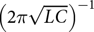 ${\left( {2\pi \sqrt {LC} } \right)^{ - 1}}$ of LC circuits depends on properly determining their geometrical dimensions. Also, high-frequency microwave resonant circuits behave like RLC elements at low frequencies, which can be excited by an external magnetic source. Analytically, using the return loss, insertion loss and bandwidth in the certain band, the lumped element values of a single meta-resonator can be obtained using Equations 5-7 [Reference Bage, Das and Murmu4, Reference Bage29].
 \begin{equation}{R} = {Z_0}\frac{{\left| {{S_{21}}\left( {j{\omega _0}} \right)} \right|}}{{2\left( {1 - \left| {{S_{21}}\left( {j{\omega _0}} \right)} \right|} \right)}}\end{equation}
 \begin{equation}{L} = 10\,{B_{3dB}}\,{Z_0}\frac{{| {{S_{21}}( {j{\omega _{0}}} )} |}}{{2\omega _{0}^{2}}}\end{equation}
 \begin{equation}{C} = \frac{2}
{10\,{B_{3dB\,}}{Z_{0}}\,| {{S_{21}}( {j{\omega _{0}}} )} |}
\end{equation}
Here,  ${\omega _0}$ is the angular frequency (rad/sec),
 ${f_0}$ is the central frequency of the WGF (
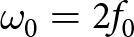 ${\omega _0} = 2{f_0}$), and B3dB is the bandwidth at the resonant frequency. Z0 is the port impedance. The values presented in Table 2 are primarily obtained from Eq. 5-7. Since the equivalent circuit of the CSRR meta-resonators with ring geometry is a series LC circuit, the dimensions of the CSRR are determined to provide the desired inductance and capacitance values. The dimensions of CSRRs are accurately optimized with the help of an “optimizer” in the simulation program with a center frequency of 6 GHz, as given in Table 2.
Fabrication of waveguide filters (WFGS) using CNC milling and SLA 3D printing methods
CNC milling method is mostly preferred in the production phase of passive microwave components (antenna, WG, T-junction, WGF, directional coupler, etc.). However, this method has several disadvantages compared to additive manufacturing methods, such as high production cost, physically heavier, difficult production in some geometries, and some materials that cannot be processed with this method. Recently, some 3D printing methods such as fused deposition modeling (FDM), selective laser melting (SLM), and stereolithography (SLA) emerge as alternatives to conventional methods such as CNC milling. The SLA method is a 3D printing method in which high-resolution and detailed 3D objects are fabricated by hardening layer by layer with a laser beam focused on a liquid photopolymer resin. In this 3D printing method, after the part is printed, curing is done using UV rays, and the part can be made more durable. To summarize the pros and cons of these two methods, the comparison of CNC Milling and SLA 3D Printing fabrication methods is given in Table 3.
Comparison of CNC Milling and SLA 3D Printing fabrication methods

All the fabrication steps of the part fabricated using the Elegoo Saturn 3 Ultra 12 K model SLA printer is given in Fig. 2. Figure 2a depicts the interface of the Chitu Box program for printing settings, and Fig. 2b shows the supported view of the part after printing. After printing, the part is kept in a washing container containing isopropyl alcohol (IPA), and then the part is kept in the curing device in Fig. 2c for 15 minutes. This curing process increases the hardening and durability of the printed part. Figure 2d shows the final version of the fabricated part. Standard photopolymer resin is used as the printing material; each layer height is set to 0.05 mm, and the bottom exposure time is set to 35 seconds.
All the fabrication steps of the part with SLA 3D printing, (a) the print settings using the Chitu Box program (b) the view of the part with supports after printing, (c) the curing process, and (d) the final view of the printed part.

The CNC milling method is easily accessible and widely used. The manufacturing tolerance is expected to be less than 25 µm for high-accuracy manufacturing. In this study, firstly, the CAD model of the designed WGF is obtained, and the created file with .stp extension is utilized in the fabrication phase. For the fabrication, aluminum 6065 material is used, and the WGF in Fig. 3a is fabricated with the help of the First MCV-800 CNC milling machine. The table dimensions of the machine are 400 × 800 mm2, and the process is performed at a high value of 6500 min/cycle. A 1.5 mm carbide (diamond) milling cutter is used to process the metal.
(a) Photo of the sanded part fabricated with the SLA 3D printing, (b) the step of metal coating, (c) the part with 2 K acrylic varnish applied over the entire surface after metal coating to prevent oxidation or corrosion on the surface of the part, and (d) the designed WG structure fabricated with CNC milling.

The part fabricated by the SLA 3D printing method must have metal coating applied to all of its surfaces in order to be used as a WGF, and the metal coating process is shown in Fig. 3. Firstly, the surface of the part is sanded precisely to reduce the surface roughness of the part (Fig. 3b). Using the spraying method, the entire surface of the WGF is homogeneously metal-coated (Fig. 3c). After the varnishing of the part, the metal coating is done in a process consisting of cleaning the surface particles, using a palladium activator, a combination of metal and plastic particles, and an alcohol solvent. Then, 2 K acrylic varnish is applied to the entire surface of the part to prevent oxidation or corrosion on the surface of the part after metal coating, and finally, the part is ready for use (Fig. 3d). Furthermore, the metal coating thickness should be several times the skin depth calculated for the operating frequency [Reference Genç, Başyigit, Göksu and Helhel33–Reference Genç, Başyigit, Göksu and Helhel36]. The most common challenges encountered in the metal coating process are the need for a varnishing process before the metal coating can be applied to the manufactured part, the drying time of the varnishing process must be waited for, and the necessity of repeating these processes to achieve a sufficient level. When these steps are not done very carefully, they present difficulties in terms of both surface roughness and production time. In this study, the surfaces of the WG structure fabricated by the SLA 3D printing method are metal coated to be several times the skin thickness, and the skin depth is calculated according to Equation 8.
 \begin{equation}\delta = \frac{1}{{\sqrt {\pi f\mu {\sigma _c}} \,}}\,\end{equation}
where f is the operating frequency and  ${\sigma _c}$ is the intrinsic conductivity of the metal. For the center frequency of 6 GHz, the skin depth can be calculated as 0.0694 μm. Moreover, while the CNC milling method is superior to the other production method in terms of temperature stability, the SLA method is superior in terms of cost and low weight. Standard SLA resin has a temperature resistance of up to 70 °C. Also, the CNC milling method is superior in terms of power handling capability, but since substrate material is used in both methods, the determining factor in terms of power handling capability is the substrate material. In applications requiring high power handling, ceramic material should be selected as the substrate instead of polymer-based material.
Simulation set-up and measurement campaign
All simulations in this study are performed via CST Studio Suite®, a 3D full-wave EM simulation program. Boundary conditions are set as Et = 0 in the ± x and ± y directions and “open add (space)” in the ± z direction shown in Fig. 4b. Excitation is applied to both terminals of the WG at 4-8 GHz using a waveguide port. The simulations are performed via a Xeon 4214 processor workstation. Frequency solver and tetrahedral mesh type are preferred in the simulation program, and the number of mesh cells varies between 1 000 000–1 500 000.
(a) Measurement setup for the performance of WGFs using different number and thickness of meta-resonators, (b) simulation setup, (c) S-parameters measurement via VNA of WGFs fabricated with CNC milling, and (d) SLA 3D printing technologies and (e) the designed meta-resonators etched by LKPF device.

The proposed WGFs are fabricated and measured to verify the simulation results with the 6 GHz center frequency. For the measurement of the WGFs, the test setup is given in Fig. 4a, and scattering parameter (S-parameter) measurements are performed with a vector network analyzer (VNA) (Fig. 4c and 4d). These measurements are performed separately for different filter orders and different thickness substrates and compared with simulation results. In all measurements, an HP Hewlett Packard model 8720C VNA operating in the 50 MHz-20 GHz range is used. Also, two waveguide-coaxial adapters and RF cables are used in the measurements. The adapters are SMA/female-type CentricRF brand CWR159SB models with a max. VSWR value of 1.20. The RF cable used is the CentricRF brand model C581-141-XXB of SMA/Male-SMA/Male type. In addition, the SOLT (Short-Open-Load-Through) calibration method, which is widely used and gives accurate results, is used to eliminate systematic errors in the measurement setup. The measurements are performed at the Industrial and Medical Applications Microwave Research and Application Center (EMUMAM) of Akdeniz University.
In this study, meta-resonators having two different substrates are etched with the Proto Laser U4 model LKPF device (Fig. 4e). The dimensions and properties of the substrates are given in Table 2. It is well known that if the dimensions are not adhered to in the milling process of meta-resonators, the inductive and capacitive values in the equivalent circuit of the meta-resonators can drastically shift, and as a result, the filter performance can change significantly. For this reason, the LPKF device with very high technical specifications is chosen for this study. Specifically, the maximum material size (x × y × z) is 229 × 305 × 10 mm3, and the minimum line and cavity size during engraving are 50 μm and 20 μm, respectively. The laser wavelength used is 355 nm with a manufacturing tolerance of ± 1.98 μm and a cutting speed of 200 mm/s.
The simulated and measured results
The surface roughness of WGFS fabricated by CNC milling and SLA 3D printing methods
The surface roughness values (R a and R z) of the WGF fabricated with two different manufacturing technologies are measured using the HOMMEL Tester T 500 device at the Innovative Technologies Application and Research Center (YETEM), Süleyman Demirel University, according to the ISO 4287 standard. The sensitivity class of the instrument is Class 1 according to DIN 4772, and the lowest roughness imaging value is 0.01 µm. R a is the roughness profile’s arithmetic mean of all absolute distances. R z is the mean maximum peak-to-valley of five successive sampling lengths within the measurement length. This indicates that the extreme values significantly impact the final value of R z more than R a. Also, in the measurements, the surface roughness of 3 different surfaces is measured: the aluminum surface fabricated by CNC, the resin surface fabricated by SLA 3D printing, and the surface obtained after metal coating. Each measurement is performed on the inner surface of the WGF. To reduce measurement errors, five measurements are made from different regions, and the average value is obtained. According to the measurement results as given in Table 4, the surface roughness values of the CNC surface, SLA resin surface, and metal-coated surface are 0.3836 µm, 0.168 µm, and 0.058 µm, respectively. As expected, the roughness of the SLA surface is lower than that of the CNC surfaces. The surface roughness of the SLA part is very low, and the roughness decreases further after the metal coating process. The EM performance of passive microwave components increases as the surface roughness decreases.
The values of average surface roughness (Ra) measured for three different surfaces

In addition to surface roughness, another significant parameter is the conductivity of the metal on the surface. As the surface conductivity increases, the EM performance of the component increases accordingly. The aluminum 6065 material used for the CNC milling has a conductivity value of 33.3 × 10⁶ S/m. For metal coating, a mixture of metals is used instead of a single metal. In particular, a mixture of antimony and silver is added to the nickel material to increase the conductivity. As it is well-known, as the metal conductivity increases in WGs, the surface resistivity decreases, and consequently the attenuation of the EM wave inside the WG decreases. Namely, the attenuation  ${\alpha _c}$ due to conductor losses in the rectangular WG can be formulated in Equation 9. This parameter is related to Rs, which is the surface resistance of the metal surface of the WG [Reference Chan, Ramer and Sorrentino37].
 \begin{equation}{\alpha _c} = \frac{{{R_s}\left( {2b{\pi ^2} + {a^3}{k^2}} \right)}}{{{a^3}b\beta k}}\end{equation}
 \begin{equation}{R_s} = \frac{{\sqrt {\omega {\mu _0}} }}{{2\sigma }}\end{equation}
where a, and b are the internal dimensions of the WG, k is the wave number, β is the phase constant, σ is the conductivity of the metal in the WG and η is the wave impedance. Also, as the surface roughness increases, it causes microscopic changes in the wave impedance on the inner surface of the waveguide. These local mismatches increase reflections and worsen the S11 value. In addition, increasing roughness lengthens the path of the surface currents. This causes the surface resistance to increase and the attenuation (S21) to be negatively affected. Therefore, as the surface roughness increases, it affects the S parameters, the filter response.
Scanning electron microscope (SEM) is a type of electron microscope that produces images by scanning a focused electron beam across the surface of a sample and provides detailed information about the surface topography and composition of the sample. In this work, the FEI Quanta FEG 250 is used to obtain SEM images of the surfaces. The 500 × and 3000 × SEM images of the surfaces of the WGFs fabricated by CNC milling and SLA 3D printing technology, as well as the surface of the WGF after metal coating, are given in Fig. 5. Accordingly, on the surface of the WGF fabricated with CNC milling technology, knife marks and micro-notches formed by regular and repetitive CNC machining can be seen on the surface. At 3000 × magnification, the characterization of the crystal structure of the material can be observed (Fig. 5a). On the surface of the WGF fabricated with SLA 3D printing technology, a certain irregularity and roughness can be observed, partially due to the layered structure (Fig. 5b). At higher magnification, pores and voids in the bonding regions between the layers are seen as small spherical particles and are a natural result of the layering process. Also, the roughness is less on the surface of the metal-coated SLA part since the metal coating gives the surface a more uniform and homogeneous appearance (Fig. 5c).
SEM image of different surfaces taken at 500 × and 3000 × magnification, (a) surface of WGFs fabricated with CNC milling, (b) surface of WGFs fabricated with SLA 3D printing before metal coating, and (c) after metal coating.

Frequency responses of the WGFS with the meta-resonators of different thicknesses
The scattering parameters of the designed and fabricated WGF are measured using VNA and compared with simulation results. The simulation and measurement results for the frequency responses of bandpass WGFs from 1st order to 5th, fabricated with CNC milling and SLA 3D printing technologies using the CSRR type meta-resonator at the center frequency of 6 GHz, are depicted in Fig. 6. Accordingly, Fig. 6a-6c shows the 1st, 3rd, and 5th order frequency responses for the thin substrate (Arlon AD 255C), while Fig. 6d-6f shows the 1st, 3rd, and 5th order frequency responses for the thick substrate (RT/Duroid 5880). When similar studies in the literature [Reference Bage, Das and Murmu4, Reference Aparicio, Hinojosa, Pereira and Melcón23, Reference Ortiz, Baena, Beruete and Sorolla27] are examined, it is reported that the measured results in this study are quite compatible with the simulated results. In general, the simulated results are slightly better than the measured results as expected. There are some possible reasons for this discrepancy between the results.
Simulated and measured frequency responses of WGFs using meta-resonators made of thin substrate (Arlon AD 255C): (a) 1st order filter, (b) 3rd order filter and, (c) 5th order filter, simulated and measured frequency responses of WGFs using meta-resonators made of thin substrate (RT/Duroid 5880): (d) 1st order filter, (e) 3rd order filter and, (f) 5th order filter.

These are errors due to impedance mismatch, errors due to the manufacturing tolerance of the WG and meta-resonator, calibration errors, losses between the coaxial-WG adapter and the filter, losses in the RF cable, losses due to the assembly of the parts, and losses due to the surface roughness of the WG structure due to the nature of the material. According to the measured results, the main losses occur at 1 and 2 between the WGF and the coaxial-WG adapter. In addition, during the formation of meta-resonators with the LKPF device, the dimensions of the geometric shapes change micro-scale due to the etching. Due to this, the inductive and capacitive loads of the meta-resonator changes, and the resonance points in the filter response are partially shifted (Fig. 6). With the ring geometry meta-resonators in this paper, the designed filters by nature have medium bandwidth. The filter order increases with each result in Fig. 6 and as the filter order increases, the selectivity (sharpness) of the filter increases, and the number of reflection zeros (RZs) also increases with the filter order.
A performance comparison of the proposed bandpass WGFs for different filter orders and two fabrication methods is given in Table 5. Accordingly, when the return loss (RL) and transmission loss (IL) of the designed WGFs are analyzed, the simulated and measured results are generally compatible with each other. Both fractional bandwidth (FBW), and quality factor (Q) are calculated using frequency points where the transmission loss is − 3 dB. In the WGFs fabricated with CNC milling, RL ranges between 27.95-40.37 dB and 27.10-30.95 dB for thick and thin substrates, respectively, in all filter orders, while in the WGFs fabricated with SLA 3D printing, RL ranges between 29.29-39.44 dB and 32.43-41.7 dB for thick and thin substrates, respectively. Similarly, for WGFs fabricated by CNC milling, IL varies between 0.06-0.34 dB and 0.34-0.97 dB for thick and thin substrates for all filter orders, respectively, and for the WGFs fabricated by SLA 3D printing, IL varies between 0.78-1.65 dB and 0.91-1.93 dB for thick and thin substrates, respectively. The obtained values are sufficient for the proposed filter to be used in many applications.
Performance comparison of the proposed bandpass WGFs for different filter orders and fabrication methods

In the WGFs by CNC milling and SLA 3D printing, FBW in all filter orders varies between 5.67-11.17% and 5.67-9.50% for thick and thin substrates, respectively. Moreover, Q for all filter orders varies between 8.96-17.65 and 10.53-17.65 for thick and thin substrates, respectively. It should be noted that there is an inverse relationship between FBW and Q. As the filter order increases using more meta-resonators, the sharpness of the filter increases, and the unwanted losses in the filter also increase.
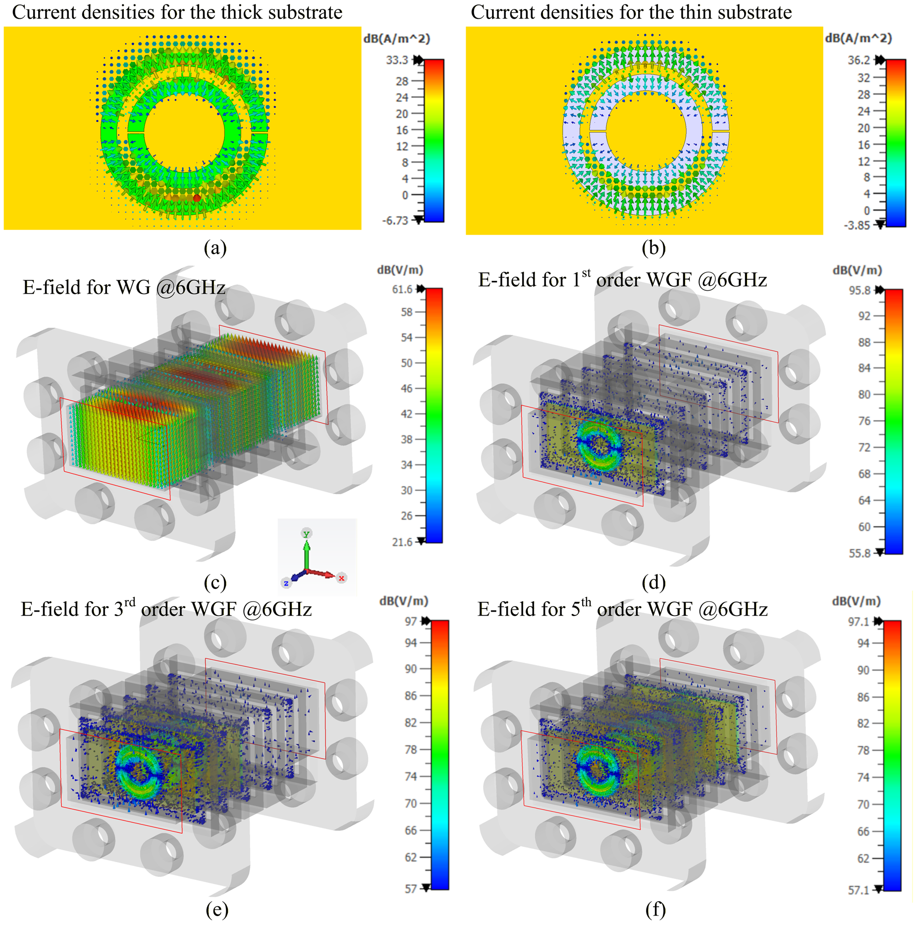
The current densities for a single meta-resonator with ring geometry for the thick and thin substrates are depicted in Fig. 7a and 7b, respectively. The highest current density in the resonator is between the two rings, with a maximum current density of 33.3 dB(A/m2) and 36.2 dB(A/m2) for the thick, and thin substrates, respectively. The current directions are opposite on the two rings depending on the phase value. Also, while the E-field distributions for the empty WG is given in Fig. 7c, E-field distribution for the 1st order, 3rd order WGF, and the 5th order WGF are given in Fig. 7d, 7e, and 7f, respectively. As seen in Fig. 7d-f, the E-field value is higher, especially in the region where the meta-resonator is located. The E-field is more intense in the space between the meta-resonators. Furthermore, the main features of the proposed WGF are summarized and quantitatively compared with the recent studies in the literature (Table 6).
The current densities for a single meta-resonator with ring geometry (a) for the thick substrate, (b) for the thin substrate, (c) E-field distribution in the empty WR-159 WG, (d) E-field distribution for the 1st order WGF (RT/Duroid 5880 substrate), (e) E-field distribution for the 3rd order WGF, and (f) E-field distribution for the 5th order WGF.
The comparison table for the performances of the wave guide filters

* In this work, the filter performance obtained from the SLA fabrication method is relatively lower than that obtained from the CNC milling method. Therefore, these values are given for the SLA fabrication method in Table 5.
Conclusion
In this study, using the novel WG structure fabricated by SLA 3D printing and CNC milling methods and CSRR type meta-resonators using different thickness substrates, the proposed C-band (4-7.5 GHz) bandpass WGFs are designed, simulated, and fabricated for the radar applications, and their performances are compared. The reason for designing WGFs with thin and thick substrates is that when access to different substrates is limited, various filters can be implemented using existing substrates with the same WG structure. Due to its modular structure, the electrical length of the designed WGFs can be changed, and the filter order and the operating band can be adjusted by means of the meta-resonators placed within the WG structure. Depending on the specific application, the designed structure can be used as a WG and a filter. Furthermore, the proposed WGFs, inserting low-loss meta-resonators into the WG structure, are an original contribution to the literature with their low return loss, high insertion loss, and high Q values. The structure fabricated by SLA 3D printing is at least 50% lighter and more cost-effective than its counterparts fabricated by CNC milling used in industry. On the other hand, the performance of the WGFs by CNC milling is slightly better than the WGFs by SLA 3D printing. As a result, according to the measured results obtained from two different fabrication methods in this study, the lightweight and low-cost SLA-printed WGFs are a good alternative to conventional filters. Moreover, the surfaces of the WGFs fabricated by the SLA method should be coated at least several times the skin depth. A metal with high conductivity should be used for the coating process. All surfaces of the part are varnished to prevent oxidation after coating and to increase the service life. Also, the surface roughness of the WGFs is well-known to affect filter performance, and the low level of surface roughness fabricated in this study is sufficient compared to both the literature and commercial equivalents.
Acknowledgement
This study is carried out within the scope of the project numbered 123E108 supported by TUBITAK (The Scientific and Technological Research Council of Turkey). Also, the metal coating of the proposed structure is carried out using ‘the infrastructure on conductive coating on plastic surfaces’ developed by Sağlamtek Aerospace Defense and DGN Coating Doğan Mazlum. We would like to thank them for their support.
Competing interests
The authors declare none.

Habib Dogan received his B.Sc. and M.Sc. degrees in Electronics Engineering from the Erciyes University in Kayseri in 1994 and 2000, respectively, and Ph.D. degree in Electronics and Communication Engineering from Süleyman Demirel University in Isparta, in 2018. He has worked as an instructor in Harran University between 1995 and 2011. He has been working as an Assoc. Prof. in Burdur Mehmet Akif Ersoy University, Golhisar High School of Applied Sciences. His current research interests are electromagnetic waves, electromagnetic propagation, microwave, and RFID applications.

Abdullah Genc received the B.Sc. degree in electrical and electronics engineering from Istanbul University, Istanbul, Turkey, in 2008, the M.Sc. degree in Mechanical engineering from Rice University, Houston, TX, USA, in 2011, and the Ph.D. degree in electronics and communication engineering from Süleyman Demirel University, Isparta, Turkey, in 2017. He has been working as an Associate Professor with the Department of Mechatronic Engineering, Isparta University of Applied Sciences, Isparta. His current research interests are electromagnetic interference (EMI), electromagnetic waves and applications, RF propagation, antenna, microwave circuit design, and dielectric measurements.

Abdulrahman Nasser Abass Abdo received his B.Sc. degree in the Department of Mechatronic Engineering at Isparta University of Applied Sciences in 2024 and has been pursuing an M.Sc. degree in the same Department. His current research interests are meta-material and radar cross-section (RCS).

Sinan Bicer is a lecturer at Akdeniz University, Elmalı Vocational School, Department of Electrical and Energy. He completed his bachelor’s degree in 2006 at Kocaeli University, Department of Electronics and Computer Education. He also earned a non-thesis master’s degree in Mechatronics from Marmara University and successfully completed his master’s degree in Mechatronics Engineering at Isparta University of Applied Sciences in 2024. His academic work focuses on information systems, communication and control engineering, robotics, and mechatronic systems. He has published articles in these fields and presented papers at international conferences.

Selcuk Helhel received his B.Sc. from Hacettepe University (1993), the M.Sc. from the Gebze Technical University (1997), and the Ph.D. from Sakarya University (2005), all in electrical engineering. S5 PLC (factory automation) programming was his initial carrier at GOLTAS Cement Factory. He got five years of experience on EMC and MIL-STD 461–462 standards, and radio telescope design projects between 1993 and 1998 at TUBITAK– MAM (UEKAE). He was with the University of Missouri – Rolla USA, in 1997, for summer school about EMC. He has been with The Department of Electrical and Electronics Engineering at Akdeniz University, since 2006. He is currently a department head in the same department. He has also been a Director of Industrial and Medical Application-Based Microwave Research Centre (EMUMAM), since 2008. His research interests include microwave propagation, Antenna Design, EMC, EMI, WiMAX, and WiMAX-based video transmission systems, and analogue communication systems.