
Introduction
Recent studies on semiconductor compound Sb2Se3 have shown that this material has many interesting properties for several applications: thermoelectric,[Reference Kim, Oh and Hyun1] energy storage devices,[Reference Xue and Fu2–Reference Luo, Calas, Tang, Li, Zhou and Mai4] solar cells,[Reference Kim, Oh and Hyun1, Reference Wang, Li, Li, Chen, Deng, Gao, Zhao, Jiang, Li, Huang, He, Song, Niu and Tang5–Reference Wen, He, Chen, Liu, Wang, Yang, Leng, Song, Zeng, Li, Li, Gao and Tang9] among others. Sb2Se3 can be prepared in polycrystalline thin films with the orthorhombic crystalline structure using standard (both atmospheric pressure or vacuum-based) thin-film growth techniques such as electrodeposition[Reference Torane and Bhosale10] or thermal evaporation,[Reference Wang, Li, Li, Chen, Deng, Gao, Zhao, Jiang, Li, Huang, He, Song, Niu and Tang5, Reference Liu, Chen, Luo, Leng, Xia, Zhou, Qin, Xue, Lv, Huang, Niu and Tang11] just to name a few. Sb2Se3 appears to be in the same class of materials as the chalcogenides Cu(In,Ga)Se2 (CIGS), CdTe, Cu2ZnSn(S,Se)4 (CZTSSe), i.e., they have excellent optoelectronic properties and are self-doped semiconductors. Their doping is intrinsic to their crystalline structure and depends heavily on growth parameters and properties. Hence, the correct identification of the Sb2Se3 crystalline structure and the correct use of the corresponding identification techniques, are of the utmost importance for the advancement of this material as an application for optoelectronic devices.
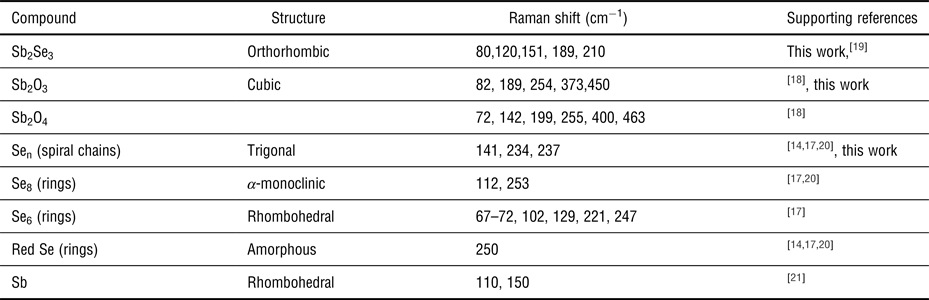
The researchers have turned their attention to Raman scattering (RS) as a powerful technique to provide qualitative information about the crystal phase of chalcogenides materials.[Reference Dimitrievska, Gurieva, Xie, Carrete, Cabot, Saucedo, Pérez-Rodríguez, Schorr and Izquierdo-Roca12, Reference Insignares-Cuello, Oliva, Neuschitzer, Fontané, Broussillou, Goislard de Monsabert, Saucedo, Ruiz, Pérez-Rodríguez and Izquierdo-Roca13] RS is widely used for the identification of main and secondary phases of chalcogenide materials as it is a non-destructive technique and allows for very fast interpretations. Moreover, in the chalcogenide materials, RS usually allows for the identification of the dominant phases without superimposition problems, as it can occur in x-ray diffraction (XRD).[Reference Salomé, Fernandes, Leitão, Sousa, Teixeira and da Cunha14] With regard to Sb2Se3, in the literature, the peaks at 190 and 250 cm−1 are usually attributed to Sb–Se and Sb–Sb bonds, respectively.[Reference Liu, Chen, Luo, Leng, Xia, Zhou, Qin, Xue, Lv, Huang, Niu and Tang11, Reference Zhang, Li, Zhang and Zhang15, Reference Zhou, Leng, Xia, Zhong, Song, Liu, Yang, Zhang, Chen, Zhou, Han, Cheng and Tang16] However, the peak about 250 cm−1 has many interpretations and conflicting origins.[Reference Zhang, Li, Zhang and Zhang15, Reference Nagata, Ishibashi and Miyamoto17, Reference Mestl, Ruiz, Delmon and Knozinger18] In fact, part of the assignment's problem arises from the fact of several selenium phases and antimony oxides having peaks close to that region as shown in Table 1. As the correct identification of which phases and structures will allow for a better understanding of the Sb2Se3 growth mechanisms and properties, in this work we will show that: (i) the 250 cm−1 peak does not belong to the Sb2Se3 phase and (ii) RS measurements done at high laser power density conditions lead to oxidation of the sample surface.
Main RS peaks of several phases that may originate during the growth of Sb2Se3. As explained further in the text, the orthorhombic Sb2Se3 is intentionally without a peak at 250 cm−1, and this region is highlighted in the other phases.

Experimental procedure
The Sb2Se3 thin films were grown according to a two-step process. Se-rich Sb–Se thin films were sputtered from a Sb2Se3 sputtering target (Stanford Advanced Materials) with a 99.99% purity, followed by a rapid thermal annealing at 300 °C with H2Se during 15 min. The composition was analyzed using Energy Dispersive Spectroscopy (EDS) and the composition ratio, (Se)/(Sb), is 1.9, which by comparing with the stoichiometric value of 1.5, implies that the overall sample is Se rich. Such fact is normal in this kind of samples as widely reported, due to condensation of Se during the cooling down of the film. Optical reflectance measurements allowed estimating a direct band gap energy of ~1.0 eV. The RS measurements were done in the backscattering configuration using a Jobin-Yvon LabRaman HR 800 spectrometer equipped with a multichannel air cooled (−70 °C) CCD detector, an Olympus BX41 microscope. The surface of the sample was focused with the help of a long working distance (25 mm) 50× objective having a numerical aperture of 0.45, allowing for a laser spot diameter of ~1.7 µm when an HeNe laser line (632.8 nm) is used as excitation source. The crystalline phase identification was complemented with XRD measurements and the results indicate that orthorhombic Pbnm (62) Sb2Se3 is the dominant phase.
Results and discussion
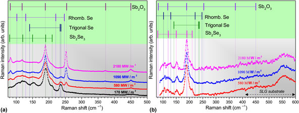
In Fig. 1(a) we present the Raman spectra of a Sb2Se3 film, measured for different power densities of the incident laser line, ranging from 170 to 2180 MW/m2, and under the same conditions of integration time and a number of repetitions. To eliminate the influence of exposure time to laser incidence during the acquisition of each Raman spectrum, a previous study (not shown) of the temporal evolution of the Raman spectrum under continuous laser incidence was carried out for each of the laser power densities used. This allowed determining the maximum exposure time (50 s) for each laser power density without changing the spectral shape. Moreover, for all our studies, the laser was turned off between each acquisition. The total laser incidence time required to perform all the spectra shown in Fig. 1(a) was about 4 min. The Raman spectra show a pronounced dependence on the laser excitation power density. We note that similar studies carried out on orthorhombic Bi2S3 nanostructures[Reference Zhao, Chua, Gan, Zhang, Peng, Peng and Xiong22] also have shown a strong dependence on power density excitation. In our case, all of the Raman spectra display peaks at 153, 189, and 210 cm−1 commonly assigned to the Sb2Se3 phase. Under low-power densities conditions, there is a double peak at 234 and 238 cm−1 which we attribute to trigonal Se,[Reference Nagata, Ishibashi and Miyamoto17] the most stable phase of selenium.[Reference Minaev, Timoshenkov and Kalugin20] The presence of such peak is consistent with the EDS measurements that showed a slight Se-rich film composition, and consequently, Se can condensate at the sample's surface,[Reference Platzer-Björkman, Zabierowski, Pettersson, Törndahl and Edoff23, Reference SeJin, Ki Hyun, Jae Ho and Kyung Hoon24] which is very common in the preparation of this kind of samples. Intriguing is the evolution of the spectrum with increasing excitation power density. It should be noted that for the lowest laser power density, no peak at ~250 cm−1 is observed, in spite of this being one of the peaks commonly reported in the Raman studies of Sb2Se3.[Reference Liu, Chen, Luo, Leng, Xia, Zhou, Qin, Xue, Lv, Huang, Niu and Tang11, Reference Zhang, Li, Zhang and Zhang15, Reference Zhou, Leng, Xia, Zhong, Song, Liu, Yang, Zhang, Chen, Zhou, Han, Cheng and Tang16, Reference Li, Chen, Zhu, Chen, Guo, Zhang, Zhang, Niu and Mai25] As the laser power density increases, together with the appearance of the ~250 cm−1 peak other peaks (~80, ~372, and ~450 cm−1) are detected whose intensities follow the increase on the intensity of the ~250 cm−1 peak, suggesting that they are likely connected. Furthermore, Fig. 1(a) shows a clear decrease of the double peak located at ~235 cm−1 with increasing RS laser power until it vanishes, for the highest power density value. On the other hand, the peak located at 190 cm−1 remains, within the experimental error, stable in position and integrated intensity but its full-width at half-maximum (FWHM) decreases by about 2 cm−1. The well-known laser heating effect always causes anharmonic effects in solids, evidenced by a broadening and a red shift of the Raman bands[Reference Weber and Merlin26] , and simultaneously, under high-power or prolonged laser irradiation, structural transitions, and crystalline changes may occur due to long-range ordering, as well as local or macroscopic ordering.[Reference Bäuerle27] At first glance, one might think that the decrease of the FWHM of the peak at 190 cm−1 is related to the local annealing of the Sb2Se3 phase, which results in an improvement in the crystalline quality of the material. However, if this would be the case, one would expect a gradual increase in intensity throughout the experiment, which was not observed. Consequently, it is unlikely that the peaks at 190 and 250 cm−1 could be correlated; thus, we do not attribute the 250 cm−1 peak to the Sb2Se3 orthorhombic phase. The appearance of the 250 cm−1 peak will be discussed further in the text.
(a) Study of Raman spectrum dependence on the laser power density excitation for a Sb2Se3 film at room temperature. Under the lowest laser power density, the peak at 250 cm−1 is absent in spite of several Sb2Se3 peaks being present. (b) Raman spectrum dependence on the excitation laser power density measured for the cross-section of the analyzed film, in a spot close to the sodium lime glass substrate (SLG). The Raman mode assignment for Sb2O3, Rhomb. Se, Trigonal Se, and Sb2Se3 were done according to references in Table 1.

By comparing the values at ~80, ~189, ~372, ~250, and ~450 cm−1 for the several phases summarized in Table 1, we concluded that these peaks correspond to a Sb2O3 phase. Previous Raman studies do not mention the power density used, and such experiments are commonly performed in an air atmosphere. Those evidences lead us to affirm that the commonly reported Raman spectra are measured under high laser power density conditions since the presence of the Raman peak at ~250 cm−1 is only observed in our measurements with high excitation power density conditions. In addition, due to the excess of Se in the films, Se phases are also a candidate to explain the existence of a Raman band at ~250 cm−1, that is related with the vibration mode of Se8 and Se6 rings.[Reference Nagata, Ishibashi and Miyamoto17] Taking into account the EDS results, showing an inhomogeneous Se distribution, different points of the sample were probed by Raman. With the objective of analyzing a region of the sample without a prolonged exposure to air, the sample was cut perpendicularly to the surface, and the Raman spectrum was immediately recorded at the fresh cross-section. Figure 1(b) relates the Raman spectrum measured, in the air, close to the glass substrate, i.e., as further away from the surface of the film as possible. We do not expect Se condensation and oxidization of a fresh cleavage cross-section. Although the signal-to-noise ratio worsens, no peak at 250 cm−1 is observed by increasing the laser power density, and the observed main peaks can only be assigned to the Sb2Se3 phase. These results indicate that in this region the film has a well-defined stoichiometry, avoiding the probability of oxidation of Sb or the contribution of selenium condensates.
All the Raman peaks observed in Figs 1(a) and 1(b) are within the expected range of frequencies when compared with the Raman frequencies reported for the lighter Sb2S3 isostructural phase.[Reference Sereni, Musso, Knoll, Blaha, Schwarz and Schmidt28] The group theory predicted, for the Sb2Se3 unit cell of five non-equivalent sites, 30 zone-center Raman actives phonon modes belong to the irreducible representation: ΓRaman = 10 A g + 10 B 1g + 5 B 2g + 5 B 3g. Removing the zero-frequency acoustic phonon modes, a total of 27 optical Raman modes are expected.[Reference Sereni, Musso, Knoll, Blaha, Schwarz and Schmidt28, Reference Caracas and Gonze29] In spite of the huge number of phonons expected, only a few peaks have been observed in the Raman studies reported so far.[Reference Zhang, Li, Zhang and Zhang15, Reference Zhou, Leng, Xia, Zhong, Song, Liu, Yang, Zhang, Chen, Zhou, Han, Cheng and Tang16, Reference Ivanova, Cernoskova, Vassilev and Boycheva19, Reference Wang, Deng and Li30, Reference Efthimiopoulos, Zhang, Kucway, Park, Ewing and Wang31] In the Raman study reported by Zhao et al.[Reference Zhao, Chua, Gan, Zhang, Peng, Peng and Xiong22] for high-quality samples of Bi2S3 material, which is also isostructural to Sb2Se3, the number of experimental Raman peaks observed is higher than the commonly observed ones for Sb2Se3. In that work, the comparison between theoretical and experimental frequencies was possible considering an adjustment process involving the entire Raman spectrum, neglecting other contributions. We note that if Sb2Se3 and Bi2S3 are isostructural with the orthorhombic crystalline phase, then, one would expect the peaks of both phases to be visible close in energy positions and with the same number of modes. Such fact is true if we discard the 250 cm−1 peak. Such occurrence is another indication supporting the hypothesis that this peak is not from the Sb2Se3 phase. As the crystalline structure of Sb2O3 is cubic, its Raman peaks should be significantly different in energy position and number of nodes compared with Sb2Se3, which is the case for the peak around 250 cm−1.
With the quality of the films investigated here, we cannot neglect other effects that may contribute to the observed Raman spectrum. To understand the RS peaks positions of Sb2Se3, we started to study the stability of the phase as a function of incident RS laser power density. In other chalcopyrite materials, like for instance CIGS and CZTS, one needs to use relatively low values of laser power density in order to avoid damage to the film itself. The damage usually comes in three forms: (i) structural changes that induce different symmetry space groups[Reference Bäuerle27]; (ii) evaporation of atoms of some elements which leads to a change in the structure[Reference Weber and Merlin26]; and (iii) incorporation and/or replacement of elements from the atmosphere, namely oxygen.[Reference Weber and Merlin26] All of these changes have the potential to be thermodynamically available by the energy delivered by the laser exposure. In this particular case, the amount of energy available to catalyze the possible changes comes from the laser power density and from relative long exposure times.
Having demonstrated further evidence that the Sb2Se3 phase should not have the 250 cm−1 peak, we will now explore its appearance. As previously referred, the appearance of new peaks, while changing the laser power density, can be a consequence of several causes. Since the FWHM values and the peak positions of the Sb2Se3 phase are kept the same as the function of laser power density, we can discard structural changes since these would change the lattice parameters and/or change the space group leading to significant changes in the RS peaks. If the 250 cm−1 peak is to be associated with a Sb2O3 phase, then, oxygen can only come from two sources: (i) oxygen already present on the sample surface due to air exposure after growth and/or (ii) oxygen present in the air.
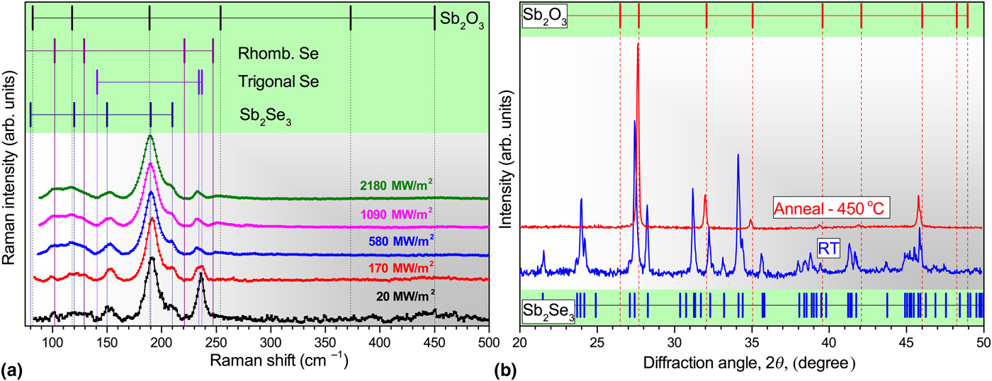
To test the oxygen origin hypothesis, we performed Raman laser power density dependence by inserting the sample in a microscope cryostat stage (Linkam 650) connected to a vacuum pump that allows to achieve a pressure of ~5 × 10⁻² mbar. In this case, the samples might locally be heated to higher temperature values due to lack of convection and thus, there is a small chance that some peak position energy shifts might occur. Figure 2(a) shows, at low laser power density the same results as in the previous test are found: (i) the Sb2Se3 can be identified with peaks at 153, 189, and 210 cm−1; (ii) the trigonal Se phase is present with a double peak at 234 and 239 cm−1. With increasing laser power density, we see the same trend as observed previously: the double peak corresponding to trigonal Se lowers significantly while the Sb2Se3 peaks suffer minor changes. At the highest laser power density values, a small peak around 250 cm−1 is present and no traces of the peak at 372 cm−1 are to be found. These results tend to indicate that under vacuum, the Se excess at the sample surface is removed; however, due to the lack of oxygen from the air, the formation of Sb2O3 is vastly reduced. The oxygen source can be attributed both to small amounts of oxygen adsorbed at the sample surface and to remaining oxygen still present in the low-vacuum conditions of the measurement.
(a) Raman laser power density dependency test in low-vacuum conditions. With increasing power density, it is observable a lowering of the peak associated with selenium and only a very small and broad peak at 250 cm−1 is found at high-power conditions. The peaks attributed to the phase Sb2Se3, 153 cm−1, 189 cm−1, and 210 cm−1, remain unchanged. The Raman mode assignment for Sb2O3 Rhomb. Se, Trigonal Se, and Sb2Se3 were done according to references in Table 1. (b) Diffractogram of the Sb2Se3 thin film at room temperature and at a temperature of 450 °C. The indexation of Sb2Se3 XRD peaks[32] is also included.
The findings of the previous experiments allow us to conclude that, contrary to the literature, the peaks at 250 and 372 cm−1 do not belong to Sb2Se3, but belong rather to Sb2O3. Furthermore, we hypothesize that the formation of the Sb2O3 is due to Se replacement by oxygen and resulting Se is simply evaporated due to its high vapor-pressure. The two-step reaction is represented by Eqs. (1) and (2):
 $$Sb_2 Se_3 (s) + Se_{2\;} (s) \to Sb_2 Se_3 (s) + Se_{2\;} (g),$$
 $$Sb_2 Se_3 (s) + 3 \cdot O_2 (g/s) \to 3 \cdot Sb_2 O_3 (s) + 3 \cdot Se_{2\;} (g).$$
This system has not been studied in detail and no trusty values of enthalpy energies are available to evaluate the reactions likelihood. These reactions fit the observed results and thermodynamic studies are needed to validate them.
To validate even further our results, a detailed XRD temperature dependence study was carried from room temperature (RT) up to 500 °C. The temperature was increased in an air atmosphere, performing effectively an in-situ air-annealing. In Fig. 2(b), we present only the results obtained at RT and 450 °C, since above 450 °C the film sublimates due to the compound high values of vapor-pressure. At low-temperature conditions, the x-ray diffractogram is dominated by the Sb2Se3 orthorhombic peaks.[32] At the temperature of 450 °C, the x-ray diffractogram starts to be dominated almost exclusively by the Sb2O3 diffraction peaks.[32] This result is further evidence that with enough energy, Sb2Se3 decomposes into Sb2O3. As in the Raman analysis, due to the significant difference in the crystalline structure between Sb2Se3 and Sb2O3, the diffraction pattern is significantly different as well.
Conclusions
In this work, we showed that the identification of Sb2Se3 using RS must be performed in low laser power density conditions, ~170 MW.m−2, in order to avoid the Se evaporation and the oxidation of the Sb2Se3 phase. The prominent peak around 250 cm−1 which is usually attributed to Sb2Se3 in the literature, belongs in fact to Sb2O3. The origin of the Sb2O3 is due to oxidation. To avoid oxidation during RS measurements and to perform more reliable measurements, at high laser excitation power conditions it is recommended to perform this technique in a vacuum or in an inert atmosphere environment. Alternatively, RS measurements of Sb2Se3 should be done at very low laser power density conditions. We note that the observation of oxidation is true for a variety of measurements that are done in air and that provide some energy to the samples like XRD, photoluminescence, photoconductivity, etc. An important observation of our work is also related with the stability of the Sb2Se3 compound: high-energy conditions, like excitation laser power or temperature, easily lead to the formation of a Sb2O3 phase, thus, synthesis processes have to account for this fact when preparing the compound.
Acknowledgments
P. M. P. Salomé acknowledges the funding of Fundação para Ciência e Tecnologia (FCT) through the project IF/00133/2015. B. Vermang has received funding from the European Research Council (ERC) under the European Union's Horizon 2020 research and innovation programme (grant agreement n° 715027). A. Shongalova acknowledges the funding of Erasmus + program 2016/17. This work was funded by FEDER funds through the COMPETE 2020 Program and by FCT – Portuguese Foundation for Science and Technology under the projects UID/CTM/50025/2013.