I. INTRODUCTION
The organization of molecules on nanometer-length scales is a necessary requirement for progress in many emerging fields of nanoscience. Although electron-beam lithography provides exceptional spatial resolution, making it the technology of choice for nanofabrication in inorganic materials,Reference Steinmann and Weaver1, Reference Zharnikov and Grunze2 the requirement to work in vacuum, combined with restricted control of chemical reactivity, has limited the extent of its application to molecular nanofabrication.Reference Golzhauser, Eck, Geyer, Stadler and Grunze3, Reference Ballav, Thomas, Winkler, Terfort and Zharnikov4 Instead, scanning probe methodsReference Sun and Leggett5–Reference Staii, Wood and Scoles22 have been used widely to pattern molecules on a variety of surfaces. They are ideally suited to the manipulation of soft matter and biomolecules because they are compatible with ambient and, in some cases, fluid operation.Reference Zhou, Bruckbauer, Ying, Abell and Klenerman19, Reference Staii, Wood and Scoles22, Reference Gu, Yam, Li and Cai23 Such methods fall into two categories. First, there are those that rely upon the mechanical placement or removal of molecules. In dip-pen nanolithography,Reference Lim, Ginger, Lee, Heo, Nam and Mirkin13–Reference Piner, Zhu, Xu, Hong and Mirkin17 an atomic force microscope (AFM) probe coated with a suitable ink is used to trace features onto a surface; the surrounding surface may then be functionalized in a second step with a contrasting molecule. In nanografting,Reference Liu, Amro, Chow and Liu10–Reference Amro, Xu and Liu12 the AFM probe is used to physically displace adsorbates from a molecular film. The features thus created may be filled in with contrasting molecules to yield a pattern. The second type of approach relies upon the initiation of a chemical reaction at the surface. Local oxidation-based approaches fall into this categoryReference Maoz, Cohen and Sagiv9: a potential difference is applied to an AFM probe in contact with a molecular surface and the local field drives bond-breaking processes leading to the oxidation of alkyl chainsReference Maoz, Frydman, Cohen and Sagiv7, Reference Maoz, Frydman, Cohen and Sagiv8 or the initiation of electrochemical reactions.Reference Fresco and Frechet24
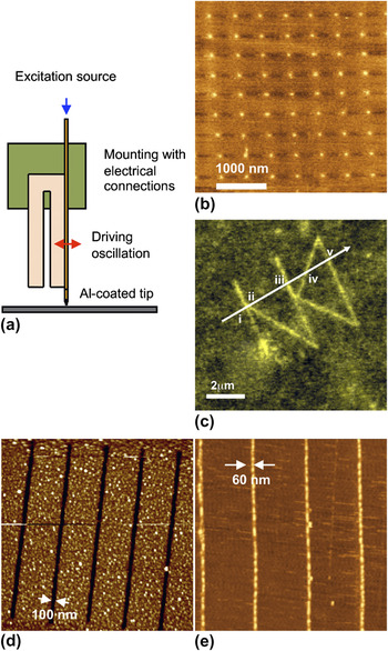
Scanning near-field photolithography (SNP)Reference Sun, Chong and Leggett6, Reference Moyer, Walzer and Hietschold25 is a second technique that falls into the latter category. In SNP, a scanning near-field optical microscope (SNOM) coupled to an ultraviolet (UV) laser is used to initiate photochemical reactions with a resolution that significantly exceeds the conventional Rayleigh limit of approximately λ/2 (see Fig. 1). Using a shear-force SNOM system, the fabrication of structures as small as 9 nm (approximately λ/30) has been demonstrated for self-assembled monolayers (SAMs) of alkylthiolates on gold,Reference Montague, Ducker, Chong, Manning, Rutten, Davies and Leggett30 and routinely it is possible to achieve resolutions in such systems that are similar to those achieved by electron-beam lithography.Reference Sun and Leggett5 There is a number of reasons why such approaches are attractive. First, photolithography has been the unrivalled methodology for device production in the semiconductor industry for four decades, an eloquent testimony to the power, precision, and reliability of optical techniques for fabrication work. Second, photochemistry is a long-established field within synthetic organic chemistry. There is a huge back-catalogue of methods to draw upon that facilitate precise, specific cleavage and modification of chemical bonds. The possibility thus exists to deploy local probe methods (e.g., SNP) to initiate highly specific chemical transformations: the integration of top–down and bottom–up methods. The development of light-directed chemical synthesis by Fodor et al.Reference Fodor, Read, Pirrung, Stryer, Lu and Solas31 has provided a model for achieving this at the micrometer scale; SNP provides the opportunity to extend this fusion to molecular length scales. Third, the explosion of interest in plasmonic techniques, and the growing interest in plasmonic lithography, provides another strong driving force. Many of the instrumental and practical issues associated with SNP are common to plasmonic lithography.
(a) Schematic diagram showing the operation of an optical fiber scanning near-field optical microscope system in shear-force mode. (b–e) Illustrations of nanopatterning by scanning near-field lithography (SNP): (b) 70-nm dots of DNA formed by covalent attachment to carboxylic acid terminated regions formed by selective photo-oxidation of benzyl chloride terminated self-assembled monolayers (SAMs) on silicon dioxide,Reference Sun, Montague, Critchley, Chen, Dressick, Evans and Leggett26 (c) lines of histidine-tagged yellow fluorescent protein formed by introduction of nanopatterned nitrilotriacetic acid groups to oligo(ethylene glycol) terminated SAMs on glass,Reference Reynolds, Tucker, Davison, Timney, Hunter and Leggett27 (d) trenches formed by etching of aluminum oxide through an alkylphosphonate SAM patterned by SNP,Reference Sun and Leggett28 and (e) gold nanowires formed by near-field sintering of a bilayer of thiol stabilized gold nanoparticles.Reference Sun, Mendes, Critchley, Diegoli, Hanwell, Evans, Leggett, Preece and Richardson29

The principal criticism of scanning probe lithography techniques is that they are intrinsically serial in nature: a probe writes one feature at a time, making the lithographic process very slow and rendering the fabrication of structures over large areas expensive. The “Millipede,” developed by Binnig and coworkers,Reference Vettiger, Despont, Drechsler, Durig, Haberle, Lutwyche, Rothuizen, Stutz, Widmer and Binnig32 provides an elegant answer to this criticism by using a large array of probes, all executing serial operations in parallel. Such a device is equivalent to a parallel processing operation when the number of probes is large enough.Reference Minne, Yaralioglu, Manalis, Adams, Zesch, Atalar and Quate33 Recently, we developed a platform to fuse the Millipede concept of parallel probe lithography with scanning near-field lithography. We call this hybrid platform the “Snomipede.” In this review, we describe the design and applications of two different prototype Snomipedes, illustrate their use to manipulate surface chemistry, and demonstrate their capacity for operation under liquid, opening the way for a reactive nanolithography that fully integrates top–down and bottom–up methods.
II. DESIGN PARAMETERS
The design of a parallel near-field lithography instrument creates a number of substantial challenges.
(i) Probe design. A probe design is required that enables light to be delivered to an array of probes simultaneously, yielding near-field excitation of the sample with minimal spillover onto the surface from far-field illumination. The dimensions of previously reported near-field probes mean that they are unsuitable for parallelization, and new excitation mechanisms were thus required for the Snomipede.
(ii) Enabling multiplexed control of writing. Although a parallel lithography tool consisting of an array of probes that wrote identical patterns simultaneously would have value, for ultimate utility it is necessary to be able to switch writing on and off at each probe independently of the others.
(iii) Control of probe–sample interactions. In order for the sample to interact with the near field associated with each probe, there must be a mechanism of ensuring that all probes remain in contact with the surface (or in very close proximity to it) simultaneously.
(iv) Wavelength of illumination. Previously, our work on SNP had utilized UV light with a wavelength of 244 nm. Because of the higher degree of complexity associated with parallel probe arrays, it was necessary to develop new approaches to patterning that were compatible with the use of near-UV radiation (>350 nm).
(v) Operation in fluid. The end goal of our program is the integration of top–down and bottom–up methods to enable the fabrication of complex, multicomponent materials. The unique capability of SNP for photochemical control of chemical reactivity would be even more powerful if integrated into a flow cell that might permit the delivery of a series of reagents, one by one. Hence, the Snomipede must be capable of functioning under fluid. Preferably, this fluid should be water, to permit processing of biomolecules.
As will be described below, we have developed two Snomipede platforms that successfully address these challenges.
A. Probe design and fabrication
The most commonly used type of near-field probe, an optical fiber operating in shear-force mode, is not suitable for parallel SNP because of the large size of the optical fiber (approximately 100 μm) and the tuning fork (approximately 1 mm), which would prevent close packing of probes. Cantilever-type probes, in which the aperture is formed at the apex of a hollow (or transparent) pyramidal probe, present an alternate approach that was adopted for the Snomipede. A commercial instrument exists that uses this configuration (WiTec, GmbH, Ulm, Germany). In that microscope, a high numerical aperture lens is placed above the probe to focus the excitation beam and ensure optimal coupling to the probe. The large size of this lens is an obstacle to close packing of probes, however. Alternate focusing systems were thus required that used microscopic light sources and/or focusing elements.
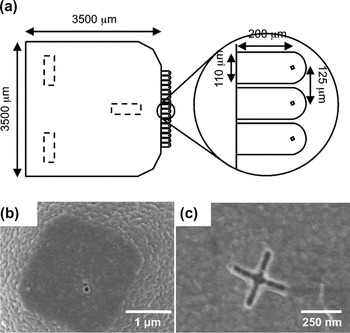
A period of 125 μm was selected for the array of apertures. An early prototype probe array was constructed in which a microlens was placed above each aperture, and a commensurate array of gallium nitride light-emitting diodes (LEDs) was used to illuminate them.Reference Kingsley, Ray, Adawi, Leggett and Lidzey34 Writing could be readily switched on and off by turning the LED on and off while the probe remained in constant contact with the sample. However, although very small structures could be formed in photoresist using this probe (with feature sizes as small as 33 nm),Reference Kingsley, Ray, Adawi, Leggett and Lidzey34 the focusing power of a microlens is limited and the working Snomipede thus utilized alternate approaches in which a laser beam was split into an array of spots using two different approaches: a liquid crystal spatial modulator combined with an objective and a digital mirror array combined with a zone-plate array (see discussion below).
The array of probes consisted of 16 identical silicon oxide cantilevers per die, with dimensions as shown in Fig. 2. At the back of the probe die, three V-grooves were formed by anisotropic etching to serve as the kinematic mounts for mounting the probe die to three hemispherical locating balls. The complete batch fabrication process is described in detail elsewhere.Reference Zhang, Docherty and Weaver35 Briefly, on a 3-inch Si (n-type, <100>) wafer, layers of 40 nm of thermal oxide and 140 nm of silicon nitride film are grown. By a combination of dry etch, photolithography, and wet chemical etch, pyramid tips and V-grooves are defined. The oxide and nitride masks on the pyramid side are stripped, and a 1-μm silicon oxide film grown by thermal oxidation. The cantilevers are defined by photolithography and wet etching, and on the back side, the thermal oxide is removed from the previously etched grooves while the oxide and nitride mask remains intact. The final step is the definition of the near-field aperture. Aluminum (150 nm) was evaporated onto the probes and then patterned by photolithography and wet etching to reduce stress on the cantilevers. The throughput of a SNOM probe (i.e., the ratio of the transmitted intensity to the intensity incident upon the aperture) is strongly dependent on the size of the aperture so it is of utmost importance that the fabrication process has a good control of the aperture sizes; near-field apertures were thus defined by a combination of electron-beam lithography and dry etching. A novel local oxidation of silicon process was adapted to avoid any overetching of Si during the Al compatible release etch. The whole 3-inch wafer consists of 168 cantilever array dice. This novel process allows highly uniform aperture definition with only 20% variation in the optical throughput (corresponding to a variation of 5 nm in aperture size). More details on the cantilever array fabrication process can be found elsewhere.Reference Zhang, Docherty and Weaver35
(a) Schematic diagram showing the dimensions of Snomipede probes. Scanning electron microscope image of (b) bath fabricated circular apertures and (c) cross-shaped apertures on tops of pyramids.

B. Instrument designs
1. Snomipede 1
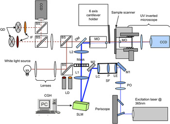
An open architecture AFM system was constructed on an optical bench as shown in Fig. 3. A commercial AFM system was used to provide basic scanning functions. Additional optical systems for UV lithography and for multiprobe detection were constructed and built around the AFM platform. The first requirement for a parallel SNOM system is the development of a convenient and reliable method to couple light to the probes. This is important because the throughput of a SNOM probe is a strong function of the aperture size and is often 10−4 or lower. The most efficient way to couple light to such small apertures is to align them with highly focused (ideally, diffraction-limited) laser spots. The generation of an array of spots with the desired spacing is thus a prerequisite for the realization of parallel SNOM device. The use of multiple laser sources would be expensive and impractical for more than two probes, since it would introduce design complexities and the requirement for a large number of optical elements. However, recent advances in computer-generated holographic projection methods to generate multiple beams from single laser source have facilitated the development of a number of powerful optical techniques, e.g., dynamic holographic optical tweezers and maskless lithography.Reference Dufresne and Grier36–Reference Ljungblad, Martinsson and Sandstrom38 Such techniques utilize a computer-addressed spatial light modulator (SLM), in which a computer-generated hologram on the SLM converts the single beam into the desired number of beams. These beams can be converted to diffraction-limited laser spots by a strongly converging lens in the beam path. We have adopted a commercial optical tweezing package (Arryx, Chicago, IL) utilizing a computer-addressed liquid crystal SLM (Boulder Nonlinear Systems, Denver, CO). The SLM was custom designed to work at wavelengths down to 350 nm. Arryx “Hotguide” software provides a graphical user interface to generate several beams (up to 400) from a single laser source via a computer-designed diffractive optical element.
Schematic diagram showing the construction of Snomipede 1.

The optical elements are shown in Fig. 3. A continuous-wave laser beam (364 nm) is passed through polarizing elements with specific orientations that depend on the desired configuration (the highest efficiency is achieved when the incoming beam has a perpendicular polarization with face of the SLM). The beam is then directed toward a spatial filter via mirror M1 where the beam is spatially filtered and expanded to 1.2 cm2. The spatial filter utilizes two well-corrected microscope objective lenses, LE and LC, and a pinhole P to provide a clean expanded laser beam on the face of the SLM.
The expanded beam is then directed toward the SLM via mirror M2 at an angle of <10° (the SLM has maximum efficiency when illuminated at 0°; the angle of 10° was used because of design constraints). A mask placed in front of the face of the SLM (dimensions 8.6 × 7.8 mm2) ensures that only the information from the SLM is transmitted to the optical train, thus eliminating any overspill of illumination outside of the screens on the cantilever probes. The face of the SLM is imaged via a telescope (lenses L1 and L2) and dichroic mirror DM (reflects UV and transmits visible) onto the exit pupil of an infinity-corrected microscope objective MO with magnification power 10x [numerical aperture (NA) 0.3] or 4x (NA 0.13).
The lenses L1 (focal length 200 mm) and L2 (focal length 250 mm) in the telescope are selected such that they expand the beam to 1.25 times so that it overfills the exit pupil of the microscope objective to avoid any vignetting of high-frequency Fourier components that diffract at large angles. This overfilling of the back focal plane of the objective is necessary to get diffraction-limited spots. The focal plane in the telescope formed by lenses L1 and L2 is conjugate to the image plane of the microscope; a mask in the conjugate plane is placed to filter out any additional stray light. The mask is formed on a quartz plate by defining 16 100-μm diameter windows in a 150 nm thick aluminum layer. The spacing between the windows depends on the choice of the objective lens, e.g., for an objective lens of 10x (focal length: 20 mm), the magnification ratio between image and conjugate plane is (25020 = 12.5), the spacing between the windows is ∼1562 μm. White light illumination (including standard white light source, beam splitters BS, and lenses) and a charge-coupled device (CCD) camera are used to monitor the cantilever probes. An inverted microscope with a UV compatible CCD camera helps to ensure that the lasers spots are coupled to the probes.
The instrument allows the precise generation of spots that can move in three-dimensional space with an accuracy of up to a few tens of nanometers depending on the choice of the optics. The cantilever chip is mounted on a six-axis translation stage for tip/tilt/rotation correction and xyz alignment of the spots with apertures with accuracy better than 30 nm. Together with the flexibility of moving each spot spatially, the alignment procedure is capable of coupling light to a large number of apertures.
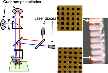
The coupling of light to the apertures alone does not guarantee that the procedure will work: to work in the near field, the apertures must be positioned <20 nm away from the surface. The Snomipede probes have a flat end approximately 1.5-μm wide, and 100-nm apertures are defined in this flat end, so operating with the cantilever tilted from the surface plane at an angle typical of an AFM (approximately 12°) would place the apertures more than 100 nm away from the surface. To address this problem, we have used a Michelson interferometer to align the cantilever array and sample surface parallel with respect to each other. We have also developed a double cantilever detection procedure, in which two separate laser beams of different wavelengths (630 and 690 nm) are reflected off two end cantilevers in the cantilever array and the resulting signal is read separately in two quadrant photodiodes QD; a sharp interference filter (IF) in front of each diode ensures that only one wavelength is read in each diode (Fig. 4). Images can be obtained simultaneously from these two end cantilevers as shown in Fig. 4. Once the end cantilevers are in contact with the same force, the other cantilevers in the array will be expected to contact the surface with a similar force. However, it was commonly noted that flattening the probe array with the interferometer and using feedback detection from the central probe is often sufficient to enable parallel lithography.
(a) Schematic diagram showing the use of a double cantilever deflection system for probe array alignment. (b) Topographical images of test specimens acquired simultaneously from two of the cantilevers in a Snomipede array.

2. Snomipede 2
SLM technology enables large arrays of spots from a single laser source to be manipulated conveniently, offering a straightforward alignment procedure for a large number of apertures and, because each diffraction-limited spot is steerable, providing a means of accommodating variations in the aperture arrays. However, at present, state-of-the-art liquid crystal SLMs are only suitable for wavelengths greater than approximately 350 nm, while there are many interesting and useful chemistries that require excitation at shorter wavelengths (e.g., thiol photo-oxidation occurs at 244 nm). Therefore, there was a need to extend the Snomipede concept to enable mid and deep UV capabilities. A second instrument (Snomipede 2) was developed that utilized zone-plate technology for delivery of light to the near-field apertures. To enable separate on/off switching of writing, light was supplied to the zone-plate array by a digital mirror array (Texas Instruments DMD Discovery 1100, Dallas, TX, with 1024 × 768 (786,432) tiltable mirrors in 16 banks of 1024 × 48). Although for the work presented here we have used 375-nm light sources, we anticipate that much shorter wavelengths can be used; indeed, zone plates can be designed to work down to x-ray wavelengths.Reference David, Kaulich, Medenwaldt, Hettwer, Fay, Diehl, Thieme and Schmahl39, Reference Djomehri, Savas and Smith40
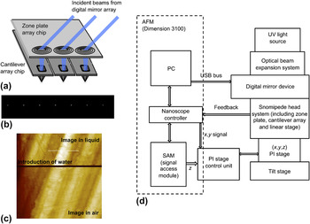
The basic principles of operation of Snomipede 2 are shown schematically in Fig. 5(a). Similar to Snomipede 1, the platform was also built around an open architecture where a commercial AFM provides basic scanning functions. However, in this design, the light from a UV diode laser (375 nm) is expanded via an optical expanding system and reflected off a digital mirror array device DMD onto the zone-plate array. The DMD consists of an array of 1024 × 768 tiltable mirrors, each 13.68 × 13.68 μm2 in size. Every micromirror has three states: floating state, ON (a tilt of +12°), and OFF (a tilt of –12°). By altering the states of the micromirrors (controlled by a C++ program), the DMD can direct light toward a zone plate or away from it and control the state of the UV beamlets (ON/OFF). Additionally, the DMD can be used to divide the UV beam into separate beams, so that each cantilever can be addressed individually, allowing lithography to be turned on and off for each lever.
The operation of Snomipede 2. (a) Schematic diagram showing the arrangement for delivery of light to the probes. (b) Array of focused spots formed by zone-plate array. (c) Topographical image acquired using a near-field probe in deflection mode while water is added. The lower portion of the image was acquired in air, and while the probe continued scanning, water was added (horizontal line), with the upper portion of the image being acquired with water in situ. (d) The organization of the control systems.

Custom-designed Brewster angle arrays of 16 zone plates were fabricated using electron-beam lithography. Using the DMD and zone-plate lens array (ZPL), an array of 16 individual diffraction-limited spots is obtained that is coincident with near-field apertures. The software-controlled DMD allows switching of individual beamlets of light corresponding to any cantilever in the array. Hence, the number of probes used at given time can be selected and controlled by appropriate selection of the DMD device. Figure 5(b) shows an array of spots formed by the ZPL, captured using a CCD camera.
C. Selection of resist
Our initial studies on near-field lithography utilized SAMs of alkylthiolates on gold surfaces.Reference Sun and Leggett5, Reference Sun, Chong and Leggett6 Selective photo-oxidation of thiolate head groups occurs following exposure to the near field, yielding weakly bound alkylsulfonate oxidation products that can be displaced in a simple solution-phase immersion step to yield molecular patterns. Alternatively, the patterned SAM can be used as a resist to fabricate features in the underlying gold film using a solution-phase etch.Reference Ducker and Leggett41 UV exposure excites reactivity specifically in the thiol head group,Reference Brewer, Janusz, Critchley, Evans and Leggett42 and the use of a monolayer resist was found to be the key to exploiting the resolution offered by near-field techniques, because of their poor depth of focus. However, thiols are by no means the only class of resist that are suitable. Monolayers of siloxanes on silicaReference Sun, Montague, Critchley, Chen, Dressick, Evans and Leggett26 and of alkylphosphonates on aluminumReference Sun and Leggett28 and titaniumReference Tizazu, Adawi, Leggett and Lidzey43 oxides have been patterned and used in a similar way either as resists for pattern transfer to the substrate or as templates for the adsorption of organic molecules, proteins, nanoparticles, and DNA. Nanoparticle films also function as effective resists for near-field lithography: nanostructures have been formed from both gold nanoparticlesReference Sun, Mendes, Critchley, Diegoli, Hanwell, Evans, Leggett, Preece and Richardson29 and C60Reference Iqbal, Sun, Hanwell, Attwood, Leggett, Preece, Richardson and Tunnicliffe44 in simple two-step processes by a combination of near-field sintering and washing to remove unmodified materials.
A drawback of these methodologies, however, is their utilization of short-wavelength radiation. In Snomipede 1, the use of a liquid crystal SLM prevented us from employing such short wavelengths. Moreover, much of the large body of work on synthetic organic photochemistry utilizes near-UV radiation. Particularly important in this regard is the work of Fodor et al. on light-directed chemical synthesis.Reference Fodor, Read, Pirrung, Stryer, Lu and Solas31 Using mask-based photolithography, in combination with photocleavable nitroveratryloxycarbonyl (NVOC) protecting group chemistries, they synthesized arrays of different compounds in a checkerboard pattern by carrying out repeated sequences of deprotection, derivatization, and then protection by NVOC. Because of the effectively quantitative photocleavage of NVOC, the sequence could be repeated many times, facilitating the construction of lengthy peptideReference Fodor, Read, Pirrung, Stryer, Lu and Solas31 and oligonucleotideReference McGall, Labadie, Brock, Wallraff, Nguyen and Hinsberg45, Reference McGall, Barone, Diggelmann, Fodor, Gentalen and Ngo46 sequences. Such methodologies were successfully commercialized and formed the basis for production of the Affymetrix GeneChip DNA sequencing system (Santa Clara, CA). Related approaches include the use of nitrophenyl caging strategies,Reference Sundberg, Barrett, Pirrung, Lu, Kiangsoontra and Holmes47, Reference Pirrung and Huang48 in which a protecting group is removed to expose a biofunctional group such as biotin, and more recently, the development of two-photon deprotection schemes.Reference Pirrung, Dore, Zhu and Rana49
Until recently, these strategies have not been used for nanofabrication. However, the possibilities are clear: a surface functional group (e.g., an amine, which offers a very wide range of subsequent conjugation strategies) capped with a photolabile protecting group may be selectively deprotected by exposure to a near-field probe, creating a localized, nanometer-scale region in which to carry out a subsequent surface chemical modification reaction. Light-directed chemical synthesis thus offers a proven paradigm from within which to attempt the unification of top–down and bottom–up fabrication methods.
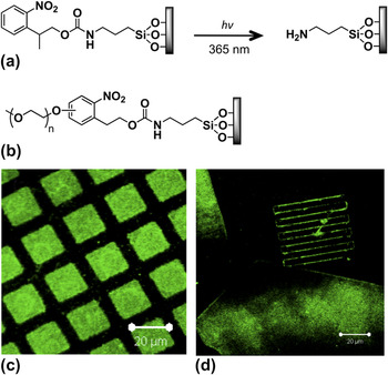
As an embodiment of this concept, we developed a strategy for nanoscale photopatterning on silicon dioxide in the near-field using nitrophenyl protecting groups. The recently introduced photosensitive 2-(2-nitrophenylpropyloxycarbonyl) (NPPOC) groupReference Pirrung, Wang and Montague-Smith50 was utilized, which is known to be photochemically removed at wavelengths >320 nm with extremely high efficiency. NPPOC-protected aminosilane films may be deprotected in the near-field to yield amine-functionalized patterns [films of aminopropyltriethoxysilane (APTES)] for conjugation to a range of molecules [see Fig. 6(a)].Reference Alang Ahmad, Wong, Ul-Haq, Hobbs, Leggett and Micklefield51 This reaction was used as a demonstration system for the Snomipede (see below).
(a) Deprotection of 2-(2-nitrophenylpropyloxycarbonyl (NPPOC)–aminopropyltriethoxysilane yields an amine-functionalized region of surface for subsequent conjugation. (b) Introduction of an oligo(ethylene glycol) substituent to the ring yields a protein-resistant surface that can be deprotected to yield an amine group for conjugation to first, biotin and second streptavidin-coated polymer nanoparticles. (Fluorescence micrographs of (c) micrometer-scale patterns and (d) 50 μm × 200 nm lines formed by SNP. The large features at the bottom and left of (d) are micrometer-scale structures formed to provide registry for subsequent SNP.

As a further elaboration of this approach, nitrophenylethoxycarbonyl-protected aminosilanes, bearing pendant oligo(ethylene glycol) (OEG) chains were synthesized [Fig. 6(b)]. Films formed from these materials exhibit very similar photochemistry to the NPPOC-protected molecules, but the presence of the OEG chains in the unexposed surfaces confers resistance to nonspecific protein adsorption.Reference Alang Ahmad, Wong, ul-Haq, Hobbs, Leggett and Micklefield52 As yet, they have not been used for parallel near-field lithography, but they illustrate how the general strategy described above may be developed to address different needs, and future work will explore their utility in parallel processes. Deprotection of these adsorbates, by illumination at 325 nm with a writing rate of 1 μm s−1, again yields amines to which further biofunctionalization of surfaces could be performed. As a demonstration, biotin was conjugated to the deprotected regions and used to bind streptavidin. Figure 6(c) shows micrometer-sized features formed by the immobilization of streptavidin-coated polymer nanoparticles loaded with a fluorescent dye on, while Fig. 6(d) shows a series of 50 μm × 200 nm lines of particles. We envisage that such bioresistant but “photoactivatable” surfaces will find many uses in biologically related applications.
D. Parallel near-field lithography
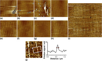
Nanostructures were written in parallel in films of NPPOC-protected aminosilane films using Snomipede 1. Light from the laser (200 mW at 364 nm) was coupled to nine probes using the SLM. The patterns were imaged using friction force microscopy (FFM),Reference Overney and Meyer53, Reference Carpick and Salmeron54 in which the lateral deflections of an AFM cantilever are measured and used to provide a measure of local variations in the surface frictional properties (Fig. 7). For macroscopic samples, the deprotected surface exhibited a water contact angle that was 15° smaller than that measured for the unprotected surface, indicating a small increase in the surface free energy. This difference was enough to utilize the high-resolution mapping abilities of FFM for the characterization of nanopatterns,Reference Alang Ahmad, Wong, Ul-Haq, Hobbs, Leggett and Micklefield51 although the contrast obtained was weak because of the small difference in surface energy (i.e., adhesiveness) of the different regions. Clear friction contrast was observed between the protected and deprotected regions: deprotected regions exhibit brighter contrast because there is a higher rate of energy dissipation here as a result of stronger tip–sample adhesion than for the surface in the unmodified regions. In images (a), (b), and (c), patterns have been formed in regions where patches of contamination can be seen; however, a clear pattern is evident outside the contaminated area. The line width for the patterns [measured from the full width half maximum (FWHM) of the cross section] was found to be 120 ± 40 nm. It is envisaged that this dimension could be reduced by forming smaller apertures in the near-field probes. However, given that the probes were writing in parallel over an area approximately 1 mm wide, this nevertheless represents a very high level of performance.
(a–i) FFM images of nine patterns formed in parallel using Snomipede 1 in a film of NPPOC-protected aminosilane. (j) Section through one of the lines. The vertical scale gives the photodetector signal, which is proportional to the friction force.

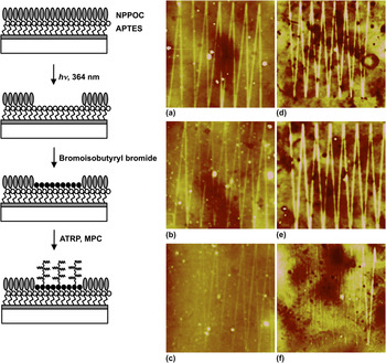
To demonstrate the capacity for subsequent synthetic elaboration of patterns formed using the Snomipede, templates were defined for the growth of nanostructured polymer brushes. NPPOC-protected aminosilane films were first photo-deprotected at 364 nm to yield amine terminal groups and these were then derivatized with bromoisobutyryl bromide, an initiator for atom-transfer radical polymerization (ATRP). Poly(2-[methacryloyloxy]ethyl phosphorylcholine) (polyMPC) brushes were then grown on the modified regions by ATRP. Figure 8 shows tapping mode AFM topographical images of two sets of patterns written with three probes in parallel by Snomipede 1. The patterns were written on two different areas of the same sample with three probes. The FWHM of the brush structures was 261 ± 20 nm, and the height of the structures was approximately 10 nm. Brush structures were also grown under similar conditions on unpatterned samples that had been completely deprotected by exposing to UV light and on micropatterned samples that had been exposed to UV light through a mask. The samples were analyzed using ellipsometery and AFM. In both cases, the height of the structure is found to be approximately 100 nm. The much smaller height of the brushes grown from the nanostructures, and the broadening of the features, suggests that the brush structures have collapsed. These observations are consistent with the work of Kaholek et al.,Reference Kaholek, Lee, Feng, LaMattina, Dyer and Zauscher55 who grew poly(N-isopropylacrylamide-co-methacrylic acid) brushes from patterns formed by electron-beam lithography, and observed reduced height, together with increased width, for brushes grown from very narrow features. Such structures may be useful in helping to understand the physics of polymer brushes, and more generally, to understand the structural dynamics of low-dimensional molecular structures.
(Left) Schematic diagram showing the procedure used to fabricate nanostructured polymer brushes by parallel near-field lithography. (a–f) AFM height images of brush structures grown from two series of samples (a–c) and (d–f) patterned in parallel. Image sizes: 27 × 27 μm2.

E. Operation in fluid
A major objective in nanotechnology is the fabrication of multiple-component patterns with nanometer-scale resolution that extend over macroscopic areas. The rapid deposition of multiple different biomolecules or organic reagents is an unsolved challenge in nanofabrication. One approach toward addressing this problem would be to construct a flow cell, in which lithographic operations could be carried out while a series of different reagents was delivered through a fluidic system. Patterning in an aqueous environment, in particular, is key to many potential biological applications.
Here, we demonstrate the ability of the Snomipede to work in a liquid environment. Snomipede 2 was used for these experiments. A simple containment device was constructed by using a microscope slide to trap a drop of water against the sample surface. The Snomipede probe array was inserted into the vertically mounted assembly, water was added from a syringe, and the probe array was observed using a CCD camera. Because water has a high surface tension and a low rate of evaporation, fluid could be contained for a period of approximately 30 min using this experimental configuration, long enough to write patterns over large areas. Light (375 nm) was coupled to near-field probes with a laser power of 128 μW directed on the whole array. The center probe was used for a standard AFM feedback to control the forces between the probes and the sample. It was possible to continue imaging during the introduction of fluid, and it was observed that the probes remained apparently unperturbed, suggesting that the probe arrays were extremely robust [Fig. 5(c)]. Typical spring constant of these probes is measured to be 180 ± 30 pN nm−1.
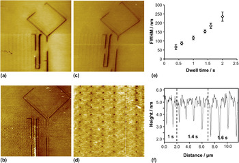
To demonstrate photolithography under water immersion, a surface substrate with a film of positive photoresist (Shipley SPR 350, Marlborough, MA, spin-coated at 7000 rpm onto glass for 60 s) was exposed in parallel. After exposure, the resist was developed ex-situ using MF-26A developer for 30 s. The samples were then characterized by AFM. Figure 9 shows a sample patterned by three probes in parallel. Large features (FWHM approximately 280 nm) were first made by scanning slowly, to provide registry structures. To test the capacity to selectively turn writing on and off, the mirrors were switched to the “off” position, directing light away from the ZPL, in a systematic way; the missing sections of the diamond and some of the larger lines thus result from periods in which the ZPL was switched “off.”
(a−c) Three AFM images showing separate patterns consisting of broad lines (as registry features) and an array of pits written in parallel by three of the 16 probes in Snomipede 2 (respectively, 40 × 40 μm2, z-contrast range 0–40 nm; 40 × 40 μm2, z-contrast range 0–100 nm; 33 × 33 μm2, z-contrast range 0–30 nm). The missing sections within the diamond and the lines result from the UV laser being directed away from the writing probes by the DMD to demonstrate an on–off capability. (d) High-magnification image of the array of dots in the lower left corner of B (16 × 16 μm2, z-contrast range 0–15 nm). (e) Variation in the full width half maximum of the pits as a function of the dwell time at a fixed laser power of 4 μW. The error bars show the standard deviations of the data. (f) Line section through the array of dots shown in (d). The dwell time decreases from top to bottom along the line. The line section shows the diameters of the spots increasing with dwell time, in line with the data in (e).

After creation of the registry structures, arrays of smaller features (dots) were then fabricated adjacent to these by holding near-field probes stationary over each location for a period of time that was varied between 0.4 and 2.0 s. The dots are faint in Figs. 9(a)–9(c) because the contrast is high on the larger registry structures. However, the dots are clear at high magnification. Figure 9(d) shows part of the array of dots in Fig. 9(b) at high magnification. Four rows of dots were fabricated using the longest dwell time, and then four rows at the next lowest, and so-on, until the bottom two rows of dots were written at the shortest dwell time. Figure 9(e) shows the mean feature size as a function of dwell time, and Fig. 9(f) is a line section through Fig. 9(d), showing how the spot size changes with the dwell time along the white line marked on the micrograph. The spots are in all cases well defined. The largest spots had diameters of 230 nm, but at best, the resolution is only 70 nm.
The depth of focus of a near-field technique is known to be poor, and the excitation spreads in a film of photoresist of finite thickness.Reference Riehn, Charas, Morgado and Cacialli56 The depth of the pits ranged from 3 to 8 nm, depending on the dwell time. Given that a resolution of 70 nm (corresponding to λ/5) could be maintained to a depth of 3 nm, it would seem that the potential for carrying out patterning in monolayers and other thin films at high resolution under water is substantial, opening the way to a reactive nanolithography in which reagents are delivered to a probe writing under fluid.
III. CONCLUSIONS
We have described two parallel near-field lithography instruments equipped with 16 probes that may be excited separately in parallel, covering a macroscopic area of 2 mm. Both a liquid crystal SLM and a digital mirror array combined with a zone-plate array are capable of delivering diffraction-limited spots to an array of near-field probes. Both configurations facilitate separate, independent switching of light to the individual probes in the array. The designs are scalable and could be adapted to facilitate the excitation of much larger arrays than have been used in the prototype Snomipede instruments described here. Feedback is readily controlled using a combination of optical deflection and interferometric methods, enabling parallel imaging to be simultaneously performed. Additionally, we have demonstrated the utility of several new chemistries for nanofabrication. The Snomipede device can be used to selectively deprotect monolayers of NPPOC-protected aminosilanes, with parallel probes operating over a region of 2 mm wide while maintaining a resolution of four orders of magnitude smaller. The photodeprotected monolayer was then functionalized with a bottom–up approach to grow nanoscale polymer brush structures. The operation of the Snomipede was demonstrated in aqueous solution on commercial positive resist films, yielding a resolution better than λ/5. We hope that the concept can be used in the future to realize the massively parallel execution of chemical transformations over macroscopic areas with high resolution.
ACKNOWLEDGMENTS
The authors thank Research Councils UK (Grant GR/C523857/1) for funding this work. LSW thanks the EPSRC for a Life Science Interface Fellowship (EP/F042590/1).